The ALU board is quite a bit more complex than the datapath board. To still be able to meet a <10x10cm² footprint, the layout had to be densified compared to the adress-datapath board.

The circuit of one slice of the ALU board is shown above. The number if dual-diodes is quite high in this design due to wide-input AOI gates used as multiplexers for the boolean units. The XNOR gate on the right side is based on a cross coupled transistor pair. No LED could be used here due to stacking of several PN junctions in the current path.
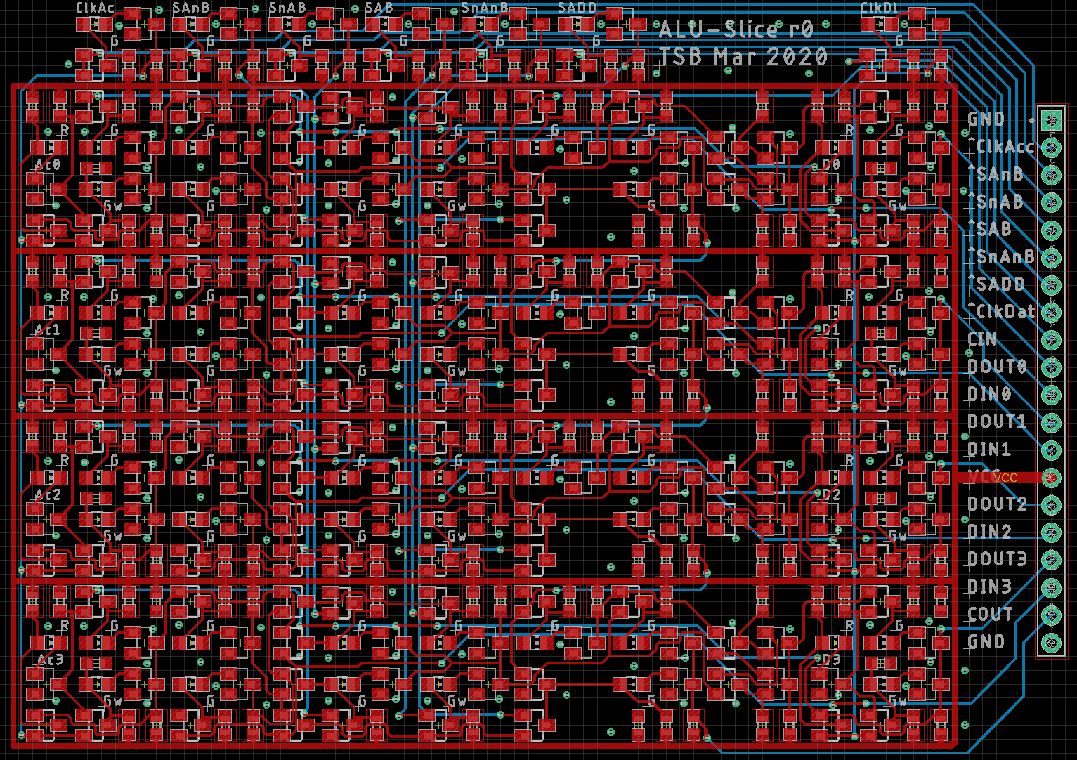
Eagle was used for the layout, making extensive use of the block functionality. Since only a two layer PCB is used, a good strategy is needed to make the layout as tight as possible.
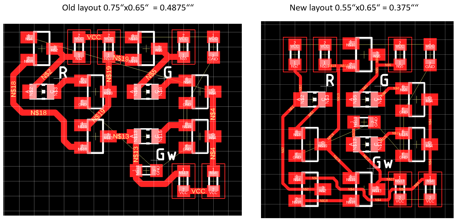
As a general rule, I used the front side for local interconnects and the power rails. Each slice was layouted with a fixed height of 0.65", which allows placing two gates between the power rails. Copper fill on both front and rear side is used for the ground plane. The rear side is only used for global routing (I/O and control signals).
After doing some estimations regarding copper line resistivity I noticed that it was possible to go to much smaller line widths.


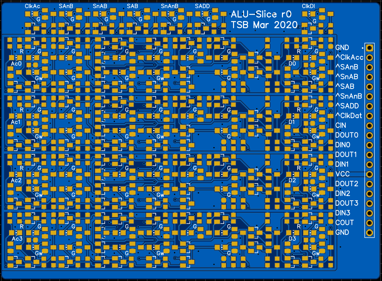
The total PCB size is 10x7 cm², only marginally larger than the adress-board. Due to the more dense layout it contains 379 devices (75xT, 95xD, 67xLED, 122xR, 20xC) , 41% more than the datapath board.
 Board render is shown above. The populated boards should arrive in a few weeks.
 Tim
Tim
Discussions
Become a Hackaday.io Member
Create an account to leave a comment. Already have an account? Log In.