-
What's in the box?
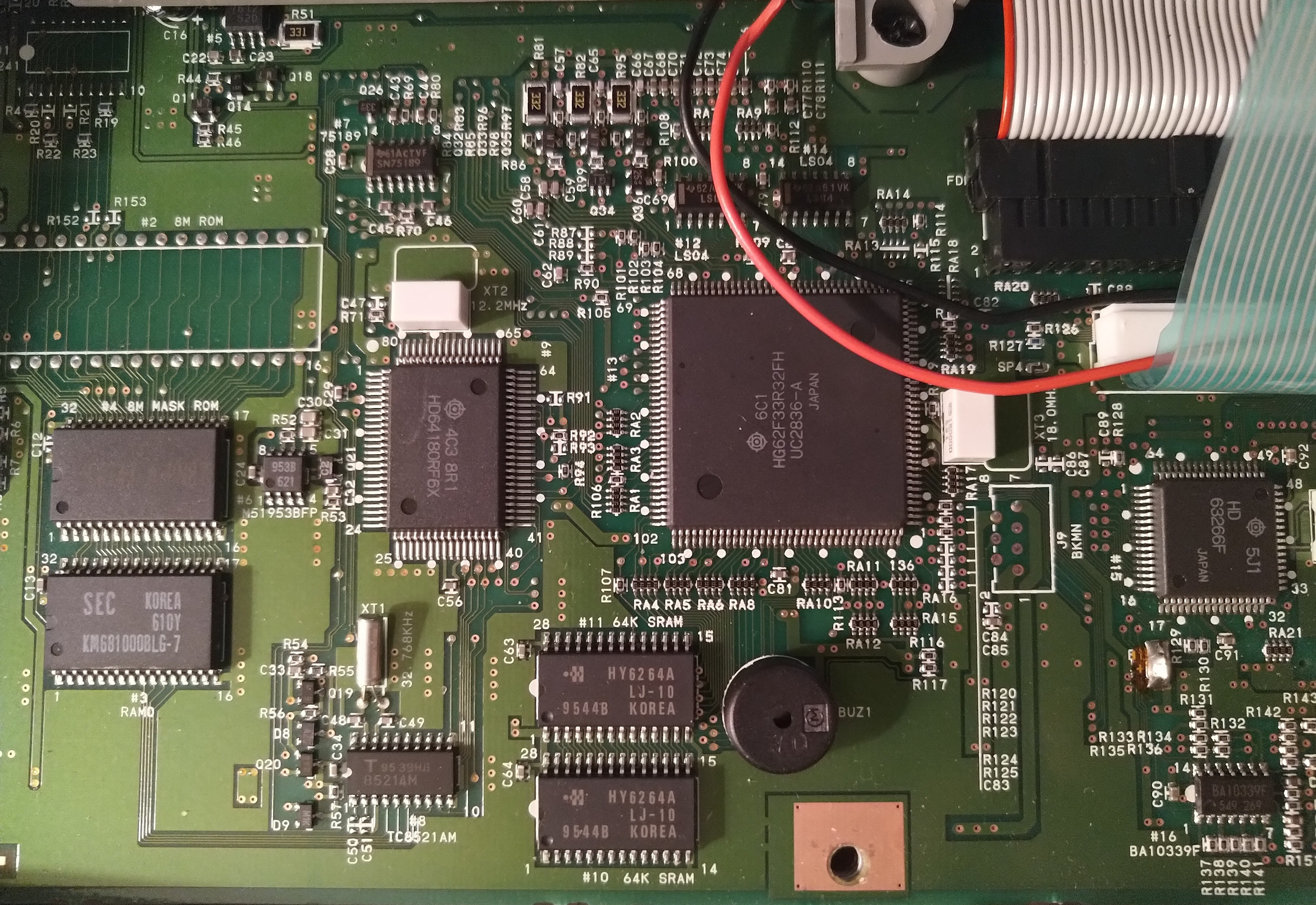
02/15/2020 at 06:23 • 1 commentBefore we try writing code, it makes sense to figure out what we can learn about the hardware we're dealing with. A good first start is to look at the motherboard and see what chips and other interesting components are there. Fortunately it's pretty easy to get to the board, just remove 3 screws from the bottom of the machine and lift the keyboard out. Below is a close-up photo of the main interesting part of the PCB, the rest of it mostly seems to be power electronics, passive components, and jacks.
Helpfully, Brother actually put the full part numbers of some of the smaller chips on the silkscreen. There's a piezo speaker, and the Tetris game on floppy disk is capable of playing some simple music, so we know the hardware is capable of more than just fixed-frequency beeps. The ROM is a small 32 pin SOIC but there are unpopulated pads for a 32 pin DIP labeled "8M ROM", perhaps some models used a DIP ROM instead of the SOIC or DIP EPROMs were used in development. The large gray ribbon cable goes to the floppy drive, the small thin one is for the keyboard.
![]()
The largest chip is a Hitachi HG62F33R32FH UC2836-A. You might expect this to be the CPU, but a quick search reveals it to be a semi-custom CMOS gate array. Given how few other chips are in the board I suspect this chip handles a lot of "glue logic", possibly interfacing to the LCD and keyboard, etc. Since this is a custom gate array the datasheet doesn't tell us much other than that the gate count is 3,297 and 128 pins are available for I/O since this is the 136 pin version of the chip. Figuring out exactly what's implemented in this would be difficult to impossible without trying to decap the chip, but that is destructive and time intensive, and something I don't have the tools for. We can probably figure out the important bits by tracing pins and looking at firmware.
To the left of the gate array is a Hitachi HD64180RF6X - This is the CPU. It's a 6 MHz Z80 derivative with a few handy built-in peripherals: Two UARTs, an MMU supporting up to 1 megabyte of memory, a two-channel DMA controller, a two-channel "programmable reload timer for output wave generation", and a few other interesting goodies. Maybe one of those programmable timers is being used as the audio output? We could probably detect that by looking for writes to the I/O ports for the timers in something that we know plays music.
Other components of note include:
- HD63266F floppy controller. I couldn't find a full datasheet for this but the floppy drive is a standard 34 pin PC drive so it's probably similar to a PC floppy controller.
- UC8247-A-PN87 mask ROM. This contains the word processor's firmware. If we can figure out the pinout of this chip we could extract the code and have a look at it.
- Samsung KM681000BLG-7 128K x8 bit SRAM. This is probably used as main RAM for the software as well as document storage.
- 2x Hyundai HY6264A-LJ10 8K x8 bit SRAM. Maybe this extra RAM is for the display?
- Toshiba TC8521AM real-time clock
- Rohm BA10339F quad comparator
- M51953BFP voltage detector/reset generator
- Three clock crystals, marked 18.0 MHz, 12.2 MHz, and 32.768 kHz. Based on location and frequency, 32.768 kHz is almost certainly for the RTC, and the 12.2 MHz is probably being divided by 2 to make a 6.1 MHz clock for the CPU. I'm not sure why 18 MHz is required, maybe it's being used to generate timing for the floppy controller or LCD.
- An unpopulated 7 pin header labeled "BKMN". Some other Super PowerNote models contained a second circuit board that could read Franklin Bookman cards, this is probably where that would connect.
- (Not Visible) A CR2032 coin cell battery for backing up the SRAM.
Brother Super PowerNote Reverse Engineering
Can we turn a cheap 90s word processor into a CP/M laptop?
 Lincoln R.