 Jacques Gagnon
Finished tracing the PCB this weekend and sent it over to PCBWay.com for a small 5 pieces test run production and one stencil. PCBWay nicely offered to sponsor the project and charged nothing for the prototypes & stencil. :)
Can't wait to receive them!! :)
Edit: Hopefully I'll get them in time for the last weekend of August:
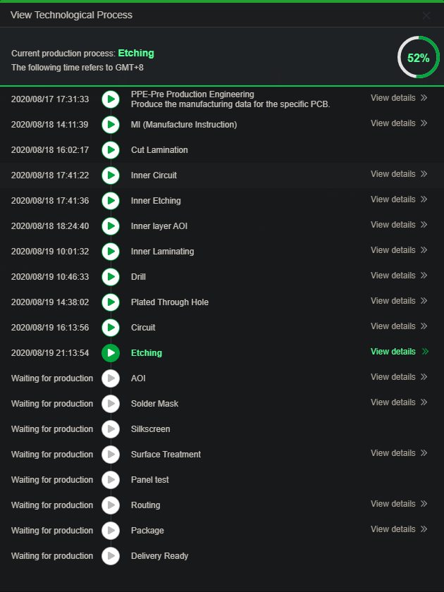
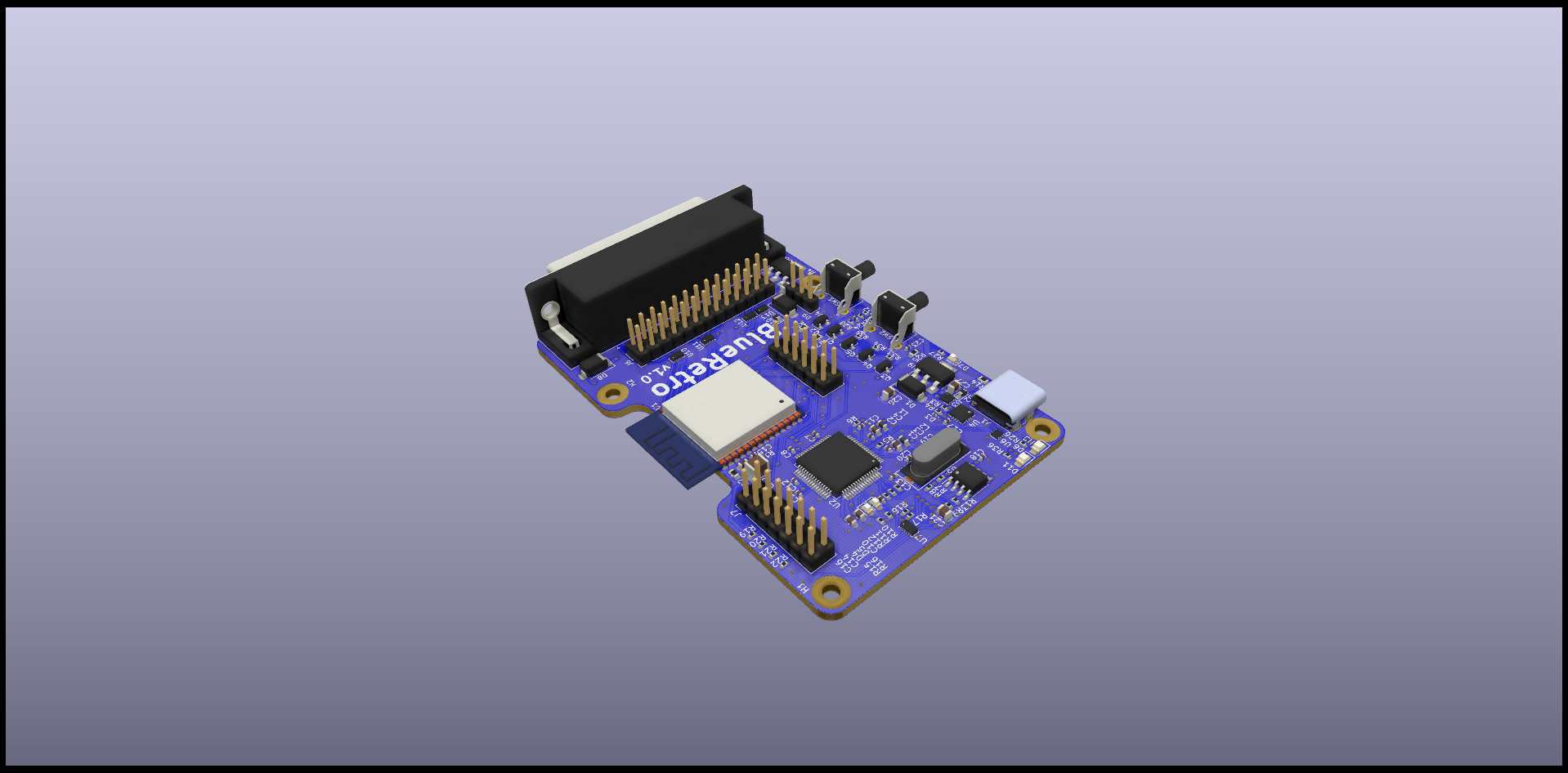
Some pictures of the final design:

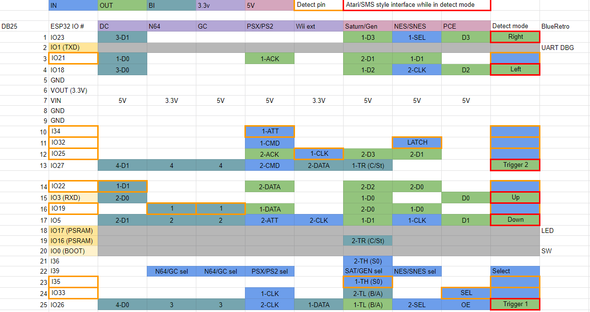
This was my first time routing a 4 layers PCB and I think it turned well. I had however to move around all the DB25 IOs to make routing more simple. No change on the software side required, but this change the cable adapter pinout.
Discussions
Become a Hackaday.io Member
Create an account to leave a comment. Already have an account? Log In.