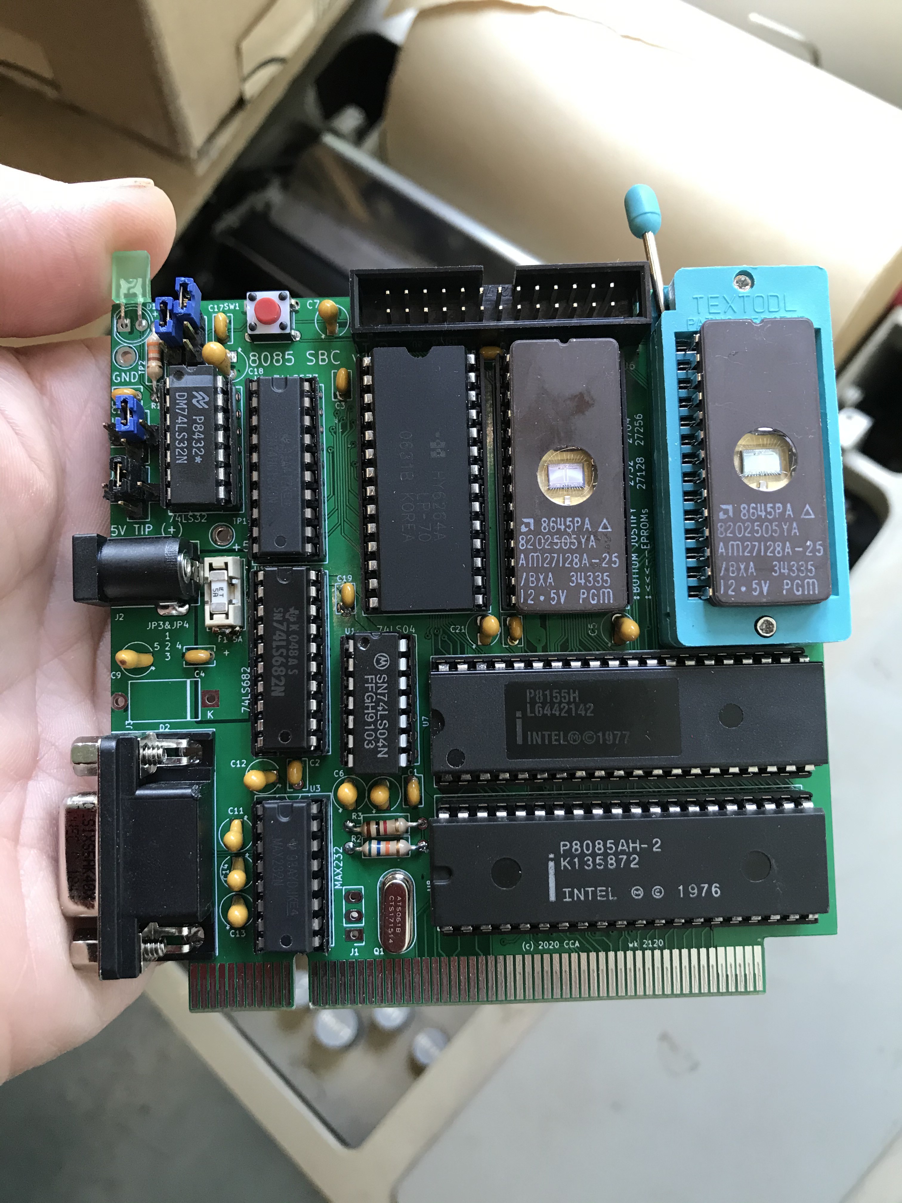
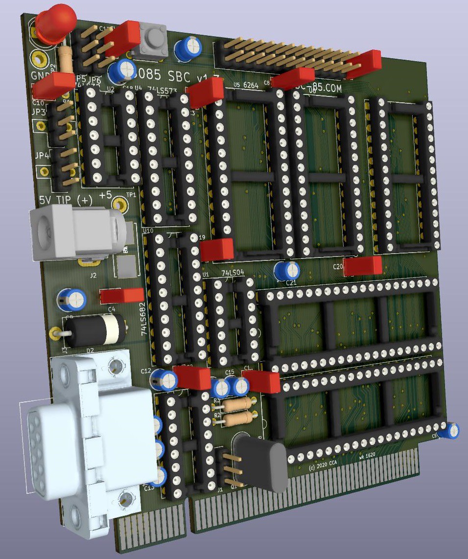
The SBC-85 CPU board is a 100mm x 100mm 2-layer with a 120 pin edge connector (mechanically PCI). The serial SID and SOD lines, via a max232, offer a RS232 serial port for communication with a resident monitor or whatever you may decide to put in firmware. The 120 expansion bus includes power, all of the 8085 status and system signals, latched address bus, and many more unused terminals for future or other board-to-board signals.
RAM is provided by a 64-kBit 6264 and an additional 2kbit in the 8155. In addition to the additional RAM, the 8155 provides an onboard timer and 22 pins of I/O. Finally, two 2732s provide onboard EPROM, one socketed on the board and the second in a ZIF for easy swap.
Power is provided by an external regulated 5V power supply through either the barrel connector or the backplane.
 Craig
Craig


Rather than think of it as a confusing time, think of the tremendous progress made with each series between 1972 and 1977. For a point of reference, look at a 1702 programmer like on the MIL MOD8 or the intel MP7 for the SIM8, now those were some serious programmers. The 1702 and 1702A both required programming with data inversion and multiple bipolar programming voltages totaling over 65 volts but the 1702A already programmed several times faster than the 1702. You would be amazed at how hot a 1702 gets when being programmed! By the time the 2708, 2716 and 2732 came around the programming voltage was already down to 25V and unipolar. Just from the 2732 to the 2732A there was a further dropped down to 21v for the 2732A and 2764. This all happened over a span of 5 years or so and while the device capacity was also going from 2kbits to 64kbits. When I pick up a 1702, 2708, 2716 or 2732A, it is hard for me not to think of the amazing history behind that chip.