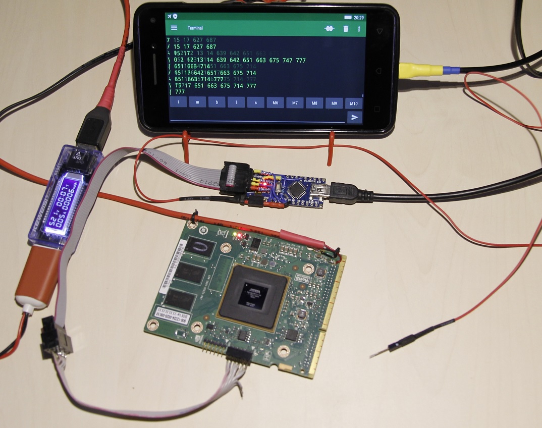
-
Follow the white rabbit.
07/05/2020 at 11:25 • 0 commentsGood things first, the device is ideal for the scenario described in the first log of the project. This device is an ideal choice, when it is necessary to determine which pin of the FPGA is connected to a contact pad reached by Probe Pin on the PCB. For this case, the speed of the JTAG interface software emulation is enough. The only drawback in this case is that we get the bit number in the Boundary Scan Register, which must be converted to the pin name with the BSDL file.
The way of working of EXTEST, EXTEST_PULSE, EXTEST_TRAIN commands suggest that the Boundary Scan Register will be initialized with a sufficiently large number of test vectors, followed by a comparison of the results. Since JTAG software emulation is used, the speed of operation is much lower than the max permissible, which is usually about 10 MHz.
It should also be noted that the limited Atmega328p memory capacity makes introduction of some new features impossible.
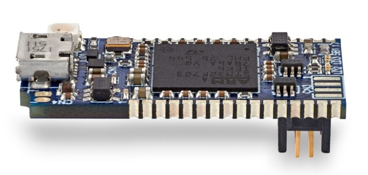
If the project is going to be developed in the future, the hardware would be implemented on STLINK-V3. There are few reasons why. Firstly, it is very affordable and costs less than 10 USD, secondly, it contains a powerful microcontroller STM32F723 .
![]()
-
Wake up, Neo... The Matrix has you...
06/14/2020 at 11:35 • 0 commentsAs noted above, the EXTEST instruction is not safe if you do not have the electronic schematic. For example, some unused pins can be connected to ground. Forced change of the state of such pins to 0 or 1, using the EXTEST command, can lead to the significant current flow. As a result the power consumed by the board under study from the power source can change. A similar situation can be observed when trying to control the state of the pins connected to the output pins of other chips or clock sources. An analysis of the power consumed by the board, in combination with the EXTEST command, will provide us with the additional information.
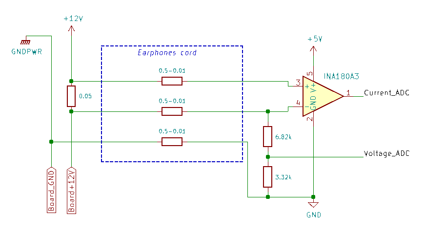
The circuit shown in the figure below was assembled in order to measure the current consumed by the board. It includes a shunt resistor and an INA180A3 current-sense amplifier.
![]()
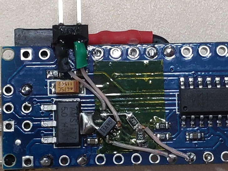
All components were mounted directly on the Arduino Nano board with the exception of the shunt resistor.
![]()
The shunt resistor was placed on the power cable. This does not comply with TI's recommendations for incorporating the INA180, but in order to verify the concept we will consider this acceptable.
The Microsoft Catapult V2 board was chosen as a test subject. Eight LEDs array is installed on the board, which are controlled by drivers via FPGA pins.
![]()
For testing we will need only a light-emitting diode LEDG[0], which is controlled by FPGA pin A11. All the information we need to control the state of this pin can be found in the BSDL file.
--BSC group 452 for I/O pin A11
 "1206  (BC_1, IOA11, input, X)," &
 "1207  (BC_1, *, control, 1)," &
 "1208  (BC_1, IOA11, output3, X, 1207, 1, Z)," &
From here everything is very simple, using the EXTEST command we are changing the state of A11, making sure that the LED is blinking, and in parallel measuring the current consumed by the board from the power source.
The oscillogram of this process is shown in the figure below. The first channel (DC coupled) of the oscilloscope is connected directly to pin A11 of the FPGA, and the second (AC coupled) to the output of INA180A3. To get a picture on the second channel as clean from noise as possible, it was required to use the function of averaging over 256 oscillograms. The total measurement time was about one minute. A similar picture is observed if the oscilloscope is synchronized with the falling edge of A11, the only difference being that the consumption current decreases. The waveform shows that the time, for which the consumed current stabilizes at a new level, is about 1ms.
![]()
That’s why, it is necessary to measure the current consumed by the board with a delay of at least 1ms. Similar measurements are presented in the figure below.
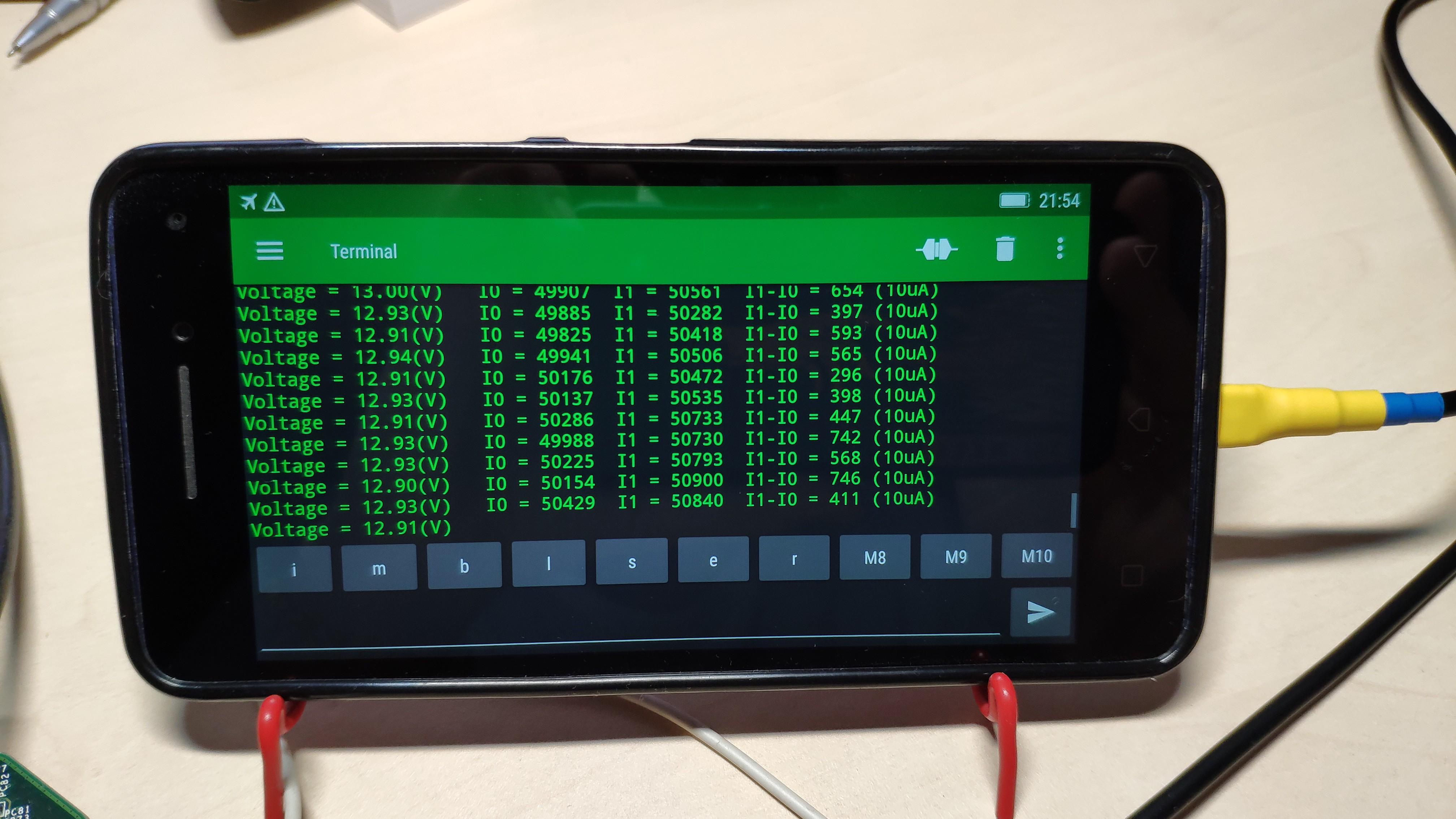
![]()
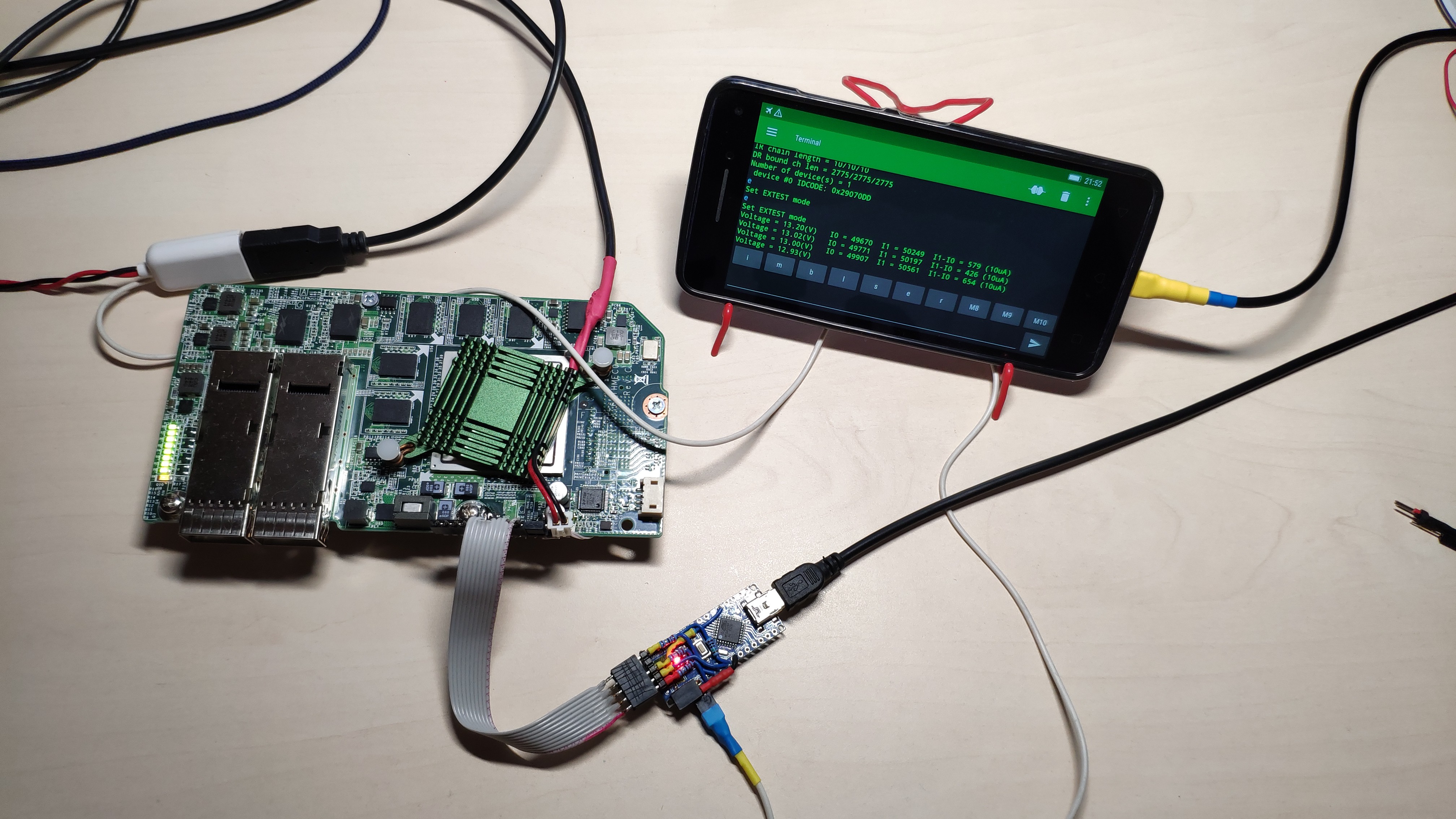
i0 - current consumed by the board in the state A11 = 0, LEDG is off.
i1 - current consumed by the board in state A11 = 1, LEDG is on.As with the oscilloscope, the data are averaged over several measurements, in this case over 100 measurements. As the results show, the system confidently registers changes in the current consumption at the level of 1%.
Obviously, the sensitivity can be improved if the recommendations for including the INA180A3 are fully implemented. It can also negatively affect the accuracy of analog measurements, in case the Arduino Nano is powered from the phone.
P.S. Arduino sketch for this log is available at https://pastebin.com/P6MCjkSU .
-
Work algorithm
05/01/2020 at 18:52 • 0 commentsThis document describes the work algorithm of the JTAG Knock-Knock(Device). All experiments were performed with a G-Sync board containing an Intel Arria V GX . The first few steps do not describe the actual usage of the Device, instead they do explain preparatory steps.
Step 1
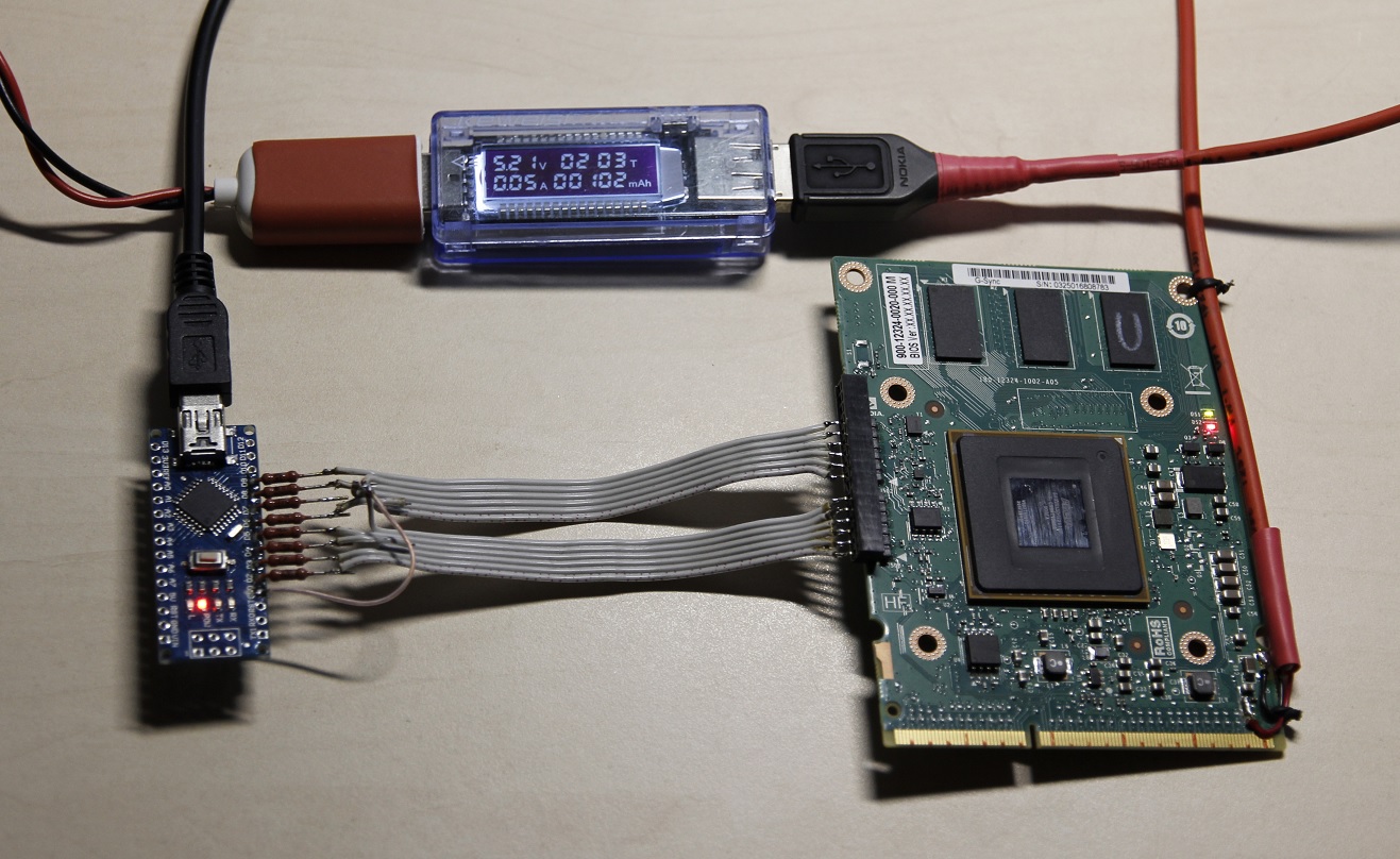
To actually start working, it is needed to determine the placement of the JTAG port on the board. First thought was about two connectors on the end of the board, that has 6 pins each, that is the one we are going to check. With a regular tester it is not difficult to determine which pins in connected to the ground. Unfortunately, it is not enough to deal with other pins. Since it is not the purpose of the Device, JTAGenum was used. Click on the link, in order to find detailed instructions on how to use it and the Arduino sketch code. Connect Arduino to the board to start searching for JTAG pins.
![Fig.1 ArduinoEnumPhoto]()
After just a few seconds of functioning we see the following result in the terminal:
The line we need is highlighted with white. That so conformity of JTAF signals and physical pins is found.
pin 1 - TMS
pin 2 - TDI
pin 4 - TDO
pin 5 - TCK
Step 2
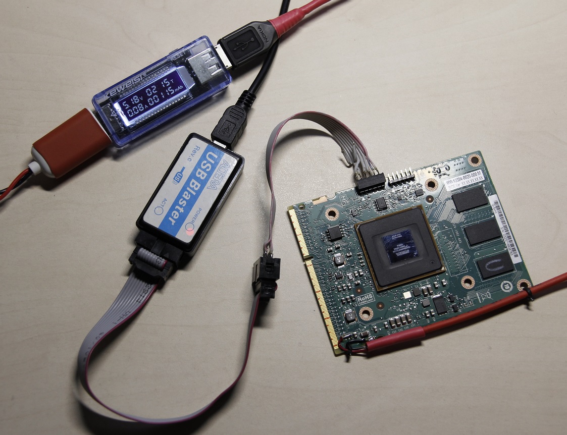
Using the information from the previous step, it is possible to make a cable to connect USB Blaster easily. Now connect the USB Blaster to the board and make sure that the Quartus Programmer sees the FPGA installed on the board.
![Fig.3 ProgrammerPhoto]()
With Quartus Programmer it is important to delete the configuration stored in flash memory. If you carefully read the documentation on the Intel Arria V GX , you may notice that the BSDL file contains information, that is relevant only for the unconfigured FPGA chip. The warning is given at the beginning and end of the BSDL file .
Once again make sure that the flash memory is clean, that so the FPGA will remain unconfigured after the board starts.
Step 3
Find the BSDL file for the Altera Arria V GX chip, in order to know following information:
attribute INSTRUCTION_LENGTH of ARRIA_V_5AGXMA3DF31 : entity is 10;
attribute BOUNDARY_LENGTH of ARRIA_V_5AGXMA3DF31 : entity is 1488;
...
"SAMPLE (0000000101), "&
This info can be added directly to the Arduino Code of the Device or entered manually while using the Device with the command "s" - Set SAMPLE Code.
Step 4
As you can see on photos below Serial USB Terminal for Android is used, though you can use any Serial Terminal, such as PuTTY for Windows/macOS. The Arduino board is connected to the phone with an OTG cable, the speed is given here .
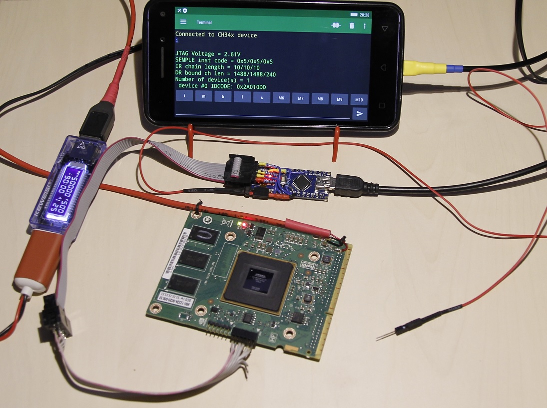
![Fig.5 JTAG_Knock_Info]()
When everything is connected properly, the command "i" - Info will give us some basic information about the chips connected to the JTAG Chain and display them on the terminal. Check carefully that the received information matches expectations.
Step 5
At this point, you can try monitoring mode by entering the command "m" - Monitor
![Fig.6 JTAG_Knock_MonitorWithoutBlock]()
The terminal will show numbers of bits that change in the Boundary scan register. These can be bits that reflect the state of real chip pins, as well as bits of some internal states. It is almost impossible to work with such a flow of information, so it is necessary to block displaying of bits that change without externally affecting the board. This can be done with entering the lock mode using the command "b" - Block.
![Fig.7 JTAG_Knock_Block]()
After a while, new lines will stop appearing on the screen, this usually takes from 5 to 20 seconds. Then we can see the bit numbers that have been added to the lock register by typing "l" - List in the terminal.
![Fig.8 JTAG_Knock_BlockListAndMonitor]()
As a result, we have a list of over twenty Boundary scan register bits that are constantly changing. This list of bits can be divided into two groups. First one contain bits, in our case, it is 0, 2, 9, 12, 13, 14, 15, 17, 21, 22, for which the only information, that can be found in the BSDL file is this:
  "0     (BC_4, *, internal, X)," &
  "2     (BC_4, *, internal, X)," &
  "9     (BC_4, *, internal, X)," &
  "12    (BC_4, *, internal, X)," &
  "13    (BC_4, *, internal, 1)," &
  "14    (BC_4, *, internal, X)," &
  "15    (BC_4, *, internal, X)," &
  "17    (BC_4, *, internal, X)," &
  "21    (BC_4, *, internal, X)," &
  "22    (BC_4, *, internal, 1)," &
Another includes the following bits 591, 627, 639, 642, 651, 663, 675, 687, 699, 714, 735, 747, 777 for which FPGA external pins were found.
  --BSC group 197 for I/O pin H6
  "591   (BC_1, IOH6, input, X)," &
  "592   (BC_1, *, control, 1)," &
  "593   (BC_1, IOH6, output3, X, 592, 1, Z)," &
  ...
  "627   (BC_1, IOF4, input, X)," &
  "639   (BC_1, IOM7, input, X)," &
  "642   (BC_1, IOL6, input, X)," &
  "651   (BC_1, IOJ4, input, X)," &
  "663   (BC_1, IOM6, input, X)," &
  "675   (BC_1, IOJ3, input, X)," &
  "687   (BC_1, ION8, input, X)," &
  "699   (BC_1, IOL4, input, X)," &
  "714   (BC_1, ION9, input, X)," &
  "735   (BC_1, IOR10, input, X)," &
  "747   (BC_1, IOP4, input, X)," &
  "777   (BC_1, IOT4, input, X)," &
Looking in the BSDL file, we can match the bits we received and external pins, as H6, F4, M7, L6, J4, M6, J3, N8, L4, N9, R10, P4, T4. These can be either clock pins or pins, that is connected to microcontroller MSP430G2553 on the board.
Step 6
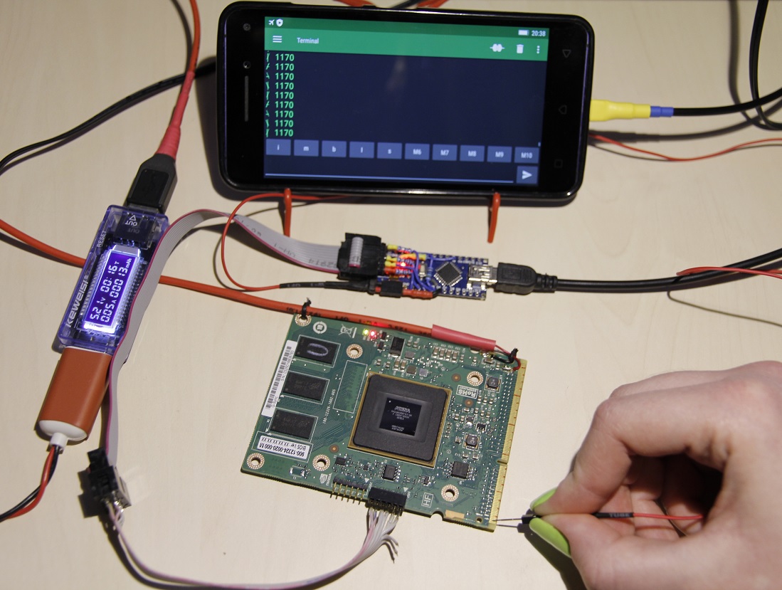
This is the final step, where the main goal is to go through all the pins on the board, in order to find a matching pin of FPGA. Entering monitor mode with command "m" and connecting a special probe pin to external one gives us information about bits on the terminal, which we find in the BSDL file and write down information about pin.
![Fig.9 JTAG_Knock_TouchPin]()
The information that was found for 1170:
--BSC group 390 for I/O pin AB18
  "1170  (BC_1, IOAB18, input, X)," &
  "1171  (BC_1, *, control, 1)," &
  "1172  (BC_1, IOAB18, output3, X, 1171, 1, Z)," &
![Fig.10 JTAG_Knock_MonitorTouchPin]()
After a few hours this process is finally over and as a result we get the file with pinout .
 MorriganR