 Pascal
After taking a closer look at the "BUS System" that the original 1-Bit-Computers used, I decided to make my own one which allowed for more flexbility. For that, I plan to use the card edge connector 6364666-1 by TE.
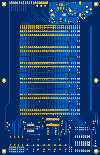
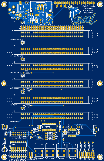
The mainboard is finally also done. Instead of no BUS slot but an expansion header, I added 4 unused expansion cards and the classic expansion header for downward compability. Also added a proper connector to add a external keyboard. The schematics are uploaded as .PDF together with a parts list.
(Also, still figuring out how this online HaDIO Web Editor works)
This is the BUS definition:
| Pin Row 1 | Name | Description | Pin Row 2 | Name | Description |
| 1 | +5V | Voltage Rail | 62 | +5V | Voltage Rail |
| 2 | GND | Voltage Rail | 61 | GND | Voltage Rail |
| 3 | INST0 | Instructions (IO Address) | 60 | PCNT0 | Program Address / Counter |
| 4 | INST1 | Instructions (IO Address) | 59 | PCNT1 | Program Address / Counter |
| 5 | INST2 | Instructions (IO Address) | 58 | PCNT2 | Program Address / Counter |
| 6 | - | Omitted Pin & Hole | 57 | PCNT3 | Program Address / Counter |
| 7 | INST3 | Instructions (IO Address) | 56 | PCNT4 | Program Address / Counter |
| 8 | INST4 | Instructions (Actual Instruction) | 55 | PCNT5 | Program Address / Counter |
| 9 | INST5 | Instructions (Actual Instruction) | 54 | PCNT6 | Program Address / Counter |
| 10 | INST6 | Instructions (Actual Instruction) | 53 | PCNT7 | Program Address / Counter |
| 11 | INST7 | Instructions (Actual Instruction) | 52 | PCNT8 | Program Address / Counter |
| 12 | CLK IN | MC14500 Clock IN (Used to define the clock) | 51 | PCNT9 | Program Address / Counter |
| 13 | CLK OUT | MC14500 Clock Out (Used for Peripherals) | 50 | PCNT10 | Program Address / Counter |
| 14 | JMP | Jump Signal (Not used) | 49 | PCNT11 | Program Address / Counter |
| 15 | RTN | Return Signal (Not used) | 48 | PCNT12 | Program Address / Counter |
| 16 | FLAG 0 | Flag 0 Signal (Not used) | 47 | PCNT13 | Program Address / Counter |
| 17 | FLAG F | Flag F Signal (Causes the Program Counter to (Preset/) Reset | 46 | PCNT14 | Program Address / Counter |
| 18 | WR/!RD | Write / Read IO | 45 | PCNT15 | Program Address / Counter |
| 19 | DATA | Data BUS | 44 | OUT0 | Output |
| 20 | RR | Result Register Output | 43 | OUT1 | Output |
| 21 | MEMWRITE | Write-Enable Signal for the Program Memory | 42 | OUT2 | Output |
| 22 | RESET CPU | Resets the CPU and IO Peripherals | 41 | OUT3 | Output |
| 23 | IN0 | Input (connected to the Result Register) | 40 | OUT4 | Output |
| 24 | IN1 | Input | 39 | OUT5 | Output |
| 25 | IN2 | Input | 38 | OUT6 | Output |
| 26 | IN3 | Input | 37 | OUT7 | Output |
| 27 | IN4 | Input | 36 | N.U. | Not used, but routed on the Main Board |
| 28 | IN5 | Input (connected to Out 5 on CPU Board by a Jumper) | 35 | N.U. | Not used, but routed on the Main Board |
| 29 | IN6 | Input (connected to Out 6 on CPU Board by a Jumper) | 34 | N.U. | Not used, but routed on the Main Board |
| 30 | IN7 | Input (connected to Out 7 on CPU Board by a Jumper) | 33 | N.U. | Not used, but routed on the Main Board |
| 31 | N.U. | Not used, but routed on the Main Board | 32 | N.U. | Not used, but routed on the Main Board |
Discussions
Become a Hackaday.io Member
Create an account to leave a comment. Already have an account? Log In.