
The Digital circuit experimental board is a set of small and delicate experimental boards designed by JLCPCB and LCSC to adapt to digital circuit experiments. The board uses Micro USB 5V input, can use mobile power, phone charger, computer, and other electrical appliances with USB interface for power supply, easy to carry, adapt to a variety of teaching environments.
1 The size of the board is 10cm*8cm which consists of the Onboard power control module, LED level display module, digital tube display module, a level selection module, single pulse generation module, 555 square wave generation module, and IC socket module, circuit PCB preview show as below;
Step 1: Power Control Module

The experimental board uses an embedded micro USB interface for power supply, which is easy for welding and provides power in a variety of ways. After power connected, a dial switch is used to control the on and off of the total power supply. When the power is on, LED10 red light is on, and the power supply works normally. The schematic diagram of the circuit is as follows
Step 2: Level Indicator Module

This part adopts 8 groups of audions to drive an LED circuit, which is connected to the outside to conduct the triode at high voltage and light up the LED; When low power is connected, the triode is disconnected and the LED is extinguished. The schematic diagram of the circuit shown as follows;
Step 3: LED Display Module

The digital tube display circuit adopts an eight-segment cathode digital tube, which is connected with current limiting resistance. When the input is a high voltage, the corresponding segment of the digital tube is lit up, while the input is low voltage, the circuit is turned off. The schematic as below;
Step 4: Level Option Module
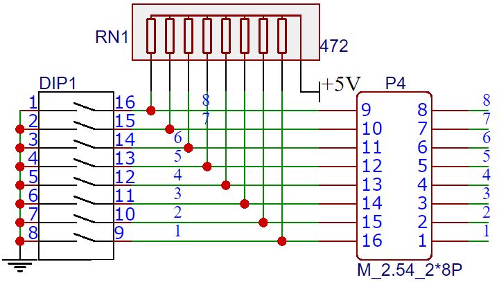
The experimental board provides eight levels output, using a dial switch to control the output, according to the silkscreen, dial to the right when the output of high level, or vice versa, schematic as below; If you need to change the schematic, click EasyEDA
Step 5: Single Pulse Module

The experimental board provides two opposite mono Pulse Generator, NAND gate, and a dial switch combine a RS Generator. The two output states are opposite, and the two output states are changed simultaneously by the dial switch. The schematic as below;If you need to change the schematic, click EasyEDA
Step 6: 555 Pulse Gernerator Module

The board provides an adjustable square pulse frequency between 10KHZ and 40KHZ that can be used as the clock input, and the output frequency is regulated by a potentiometer, the schematic as below; If you need to change the schematic, click EasyEDA
Step 7: IC Socket Module


In order to adapt to the functional verification of a variety of chips, two DIP14 sockets are provided on the experimental board, in which the seventh pin is connected with GND by default, the 14th pin is connected with VCC by default, and the other pins respectively lead out two-row pins for use.
There are also two DIP16 sockets. The corresponding eighth and 16th pins are connected with GND and VCC respectively. The rest pins also lead to two rows of pins. In addition, some of the pin arrangement of the chip is irregular, and a DIP20 socket is provided on the board. This socket is not connected with GND and VCC, and is connected according to the pin arrangement of the chip in the experiment; The schematic is below.If you need to change the schematic, click EasyEDA
 mrdiytechmagic
 Denis
Denis
 Alexander Williams
 Silícios Lab