 Tijl Schepens
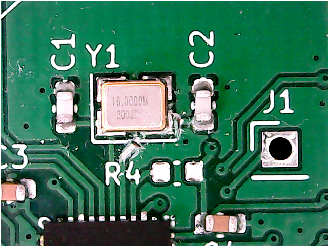
After some measurements I found out that on one pin of the two pins there was no oscillating signal. It seems I made a mistake while drawing the schematic in KiCAD. I've selected a crystal symbol which has only two pins. These two pins got connector to pads 1 and 2 of the footprint. But the crystal is connected between pads 1 and 3 of the footprint.
The only option is to do some patching using some wire.
First cut the tracks:
Then re-wire using some patching wires:
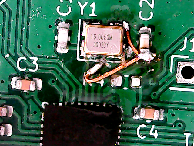
I did not bother to connect the other two pads to GND. They are now floating. This is bad for EMC, but at the moment I don't really care. As long as it works I'm happy :-)
Discussions
Become a Hackaday.io Member
Create an account to leave a comment. Already have an account? Log In.