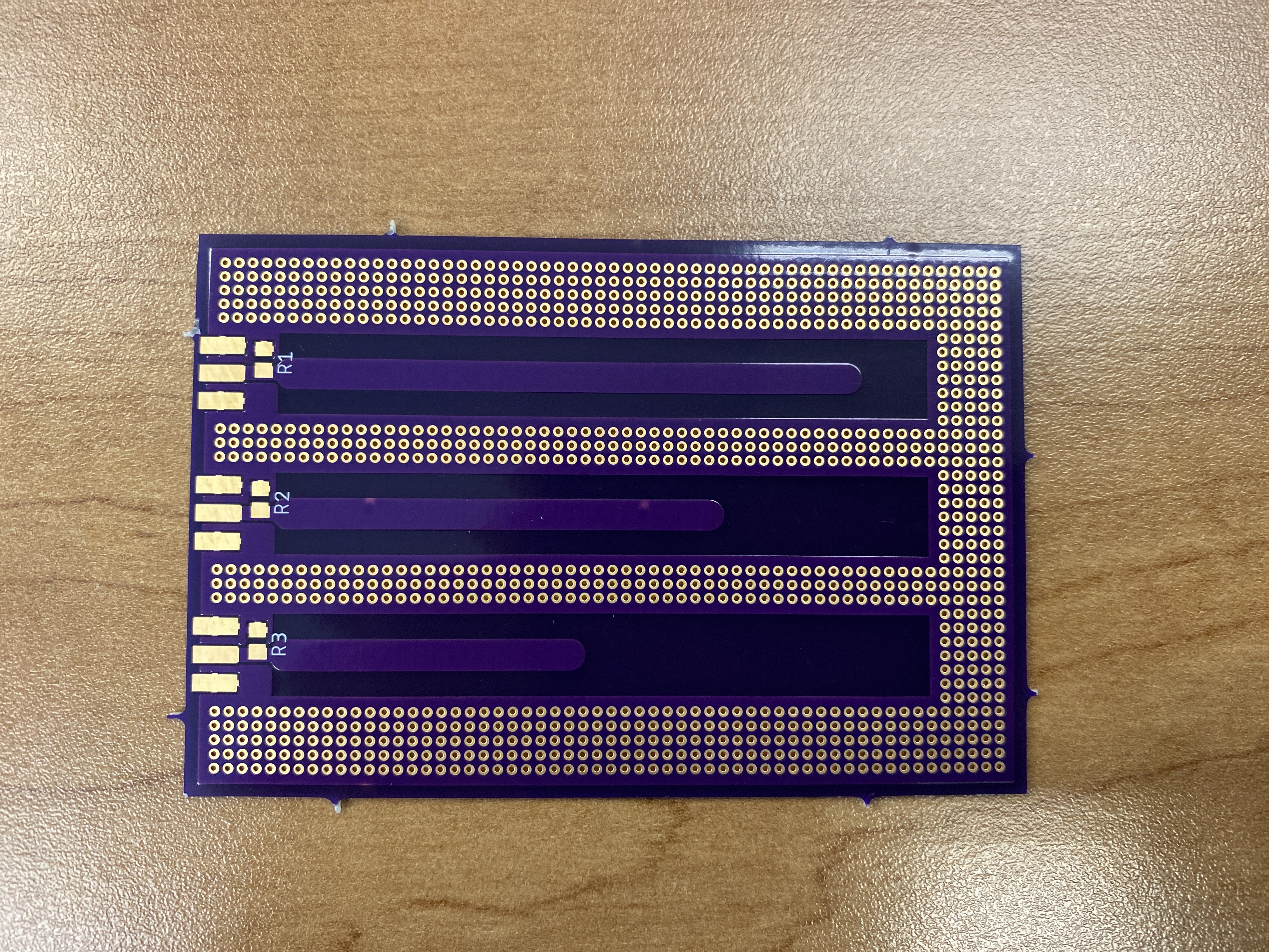
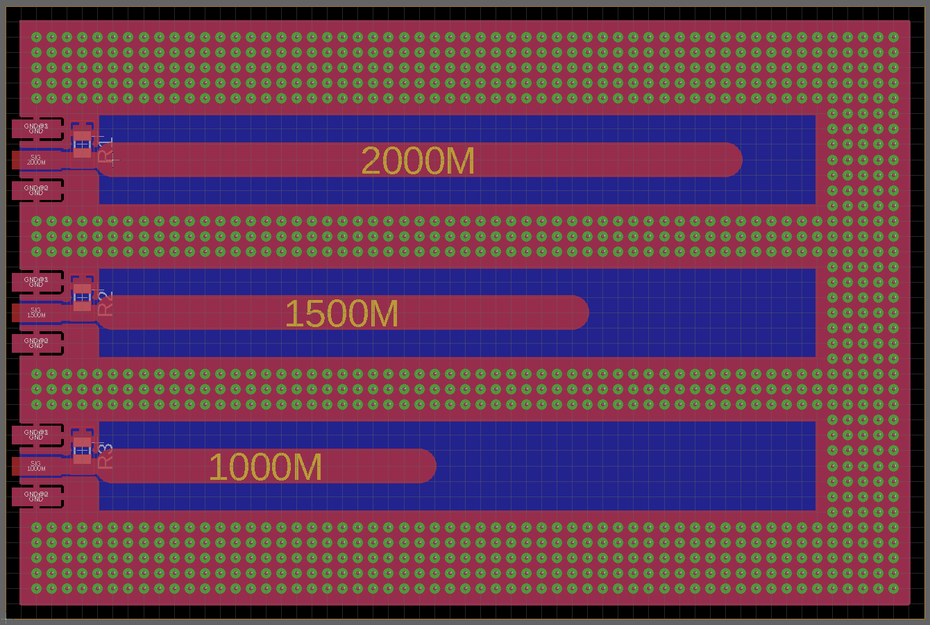
This is project is part of the Radio Astronomy SDR DAS project.
0%
0%
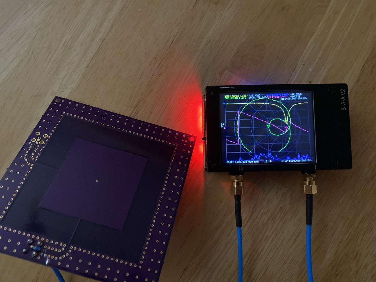
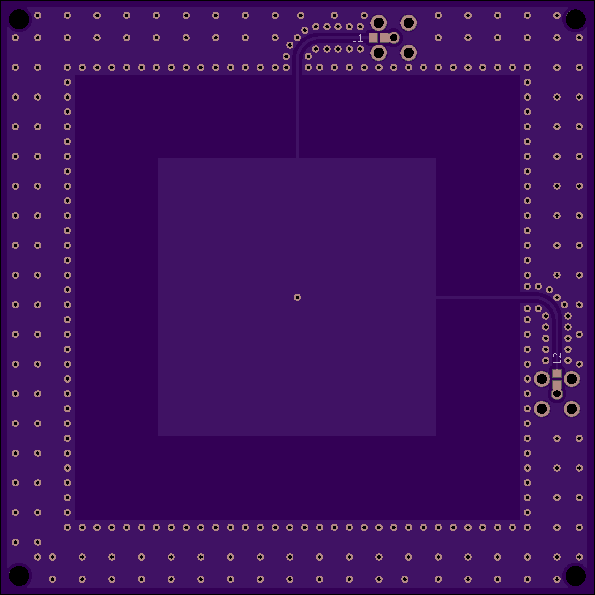
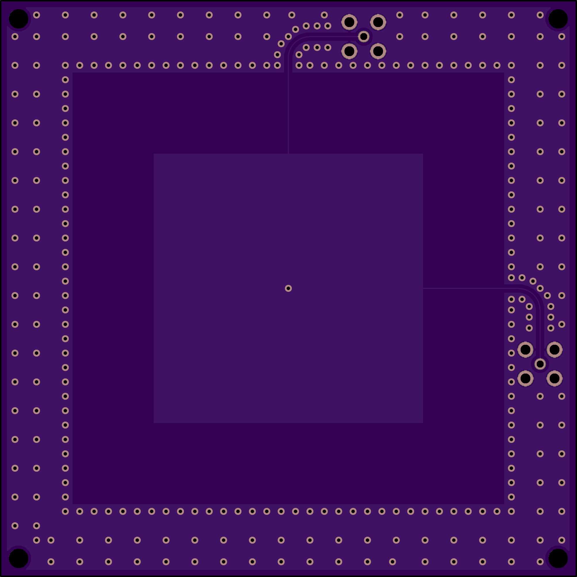
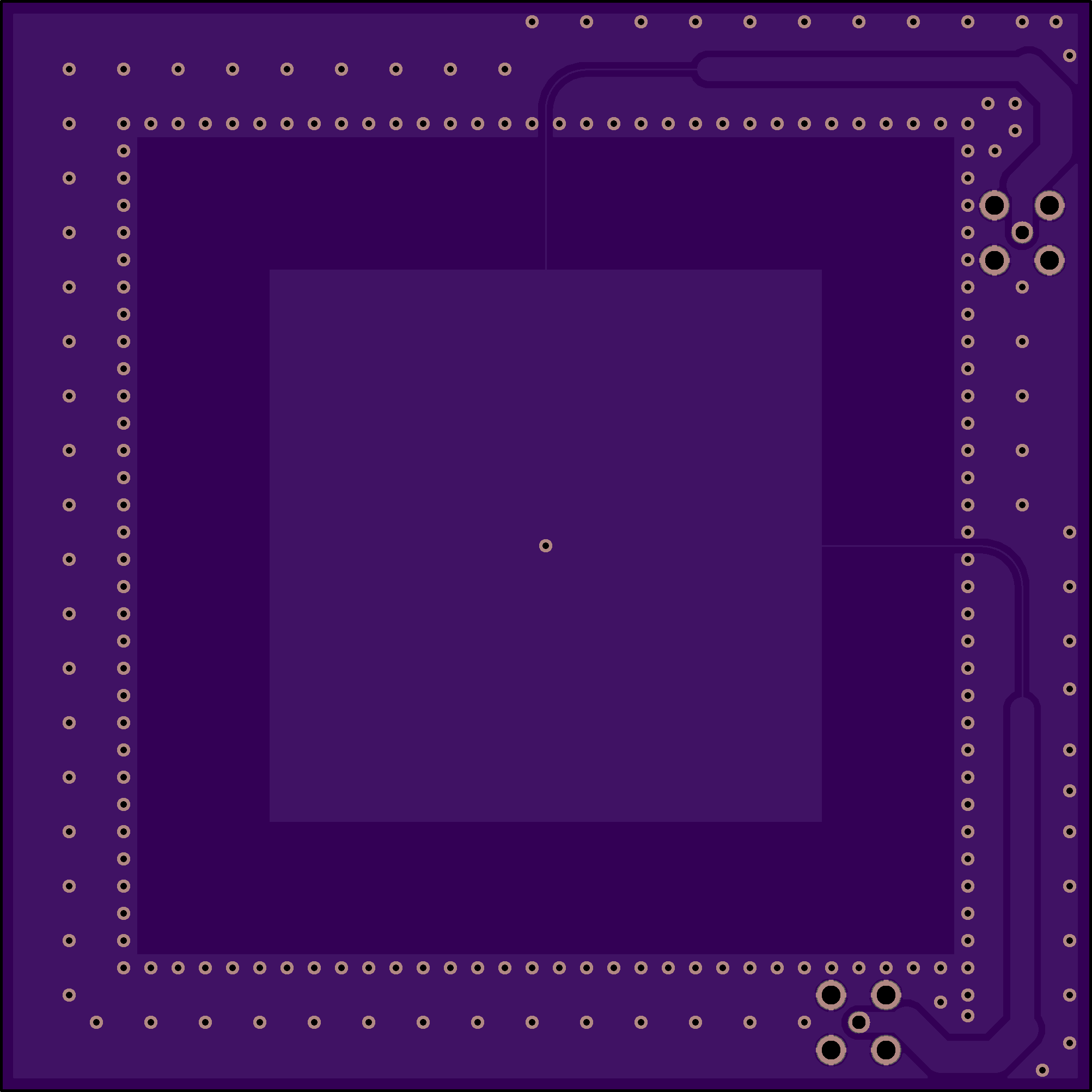
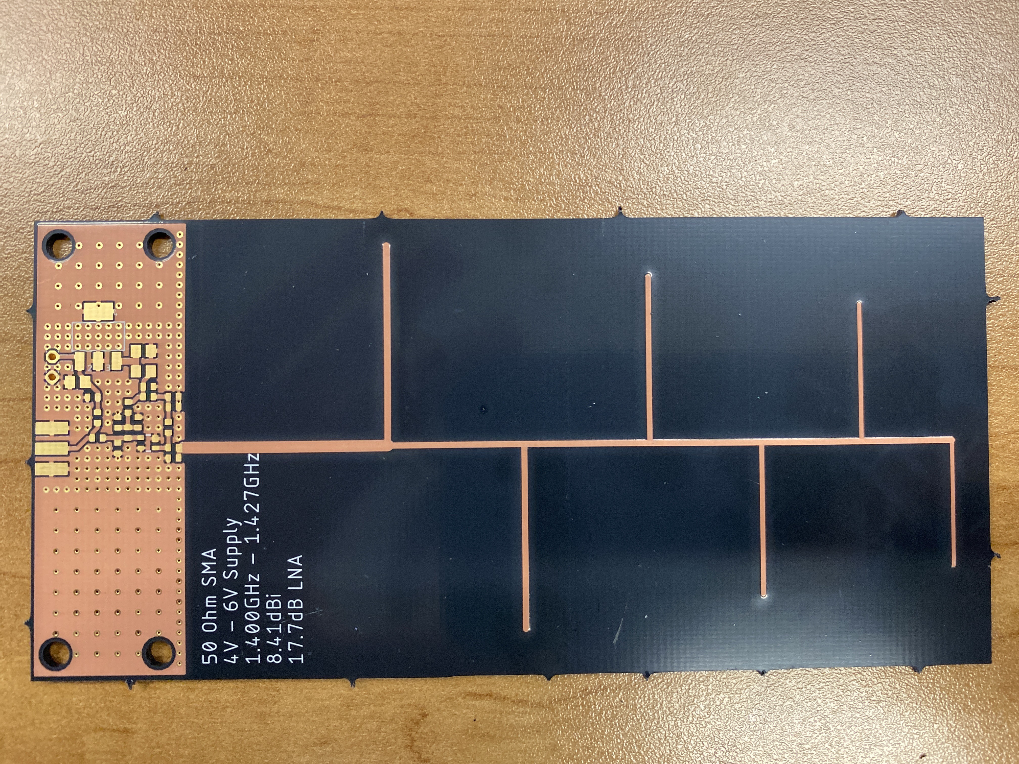
1.420 GHz Antenna
With on-board matching network.
Become a Hackaday.io member
Already have an account? Log in.
Just one more thing
To make the experience fit your profile, pick a username and tell us what interests you.
Pick an awesome username
hackaday.io/
Your profile's URL: hackaday.io/username. Max 25 alphanumeric characters.
Pick a few interests
Projects that share your interests
People that share your interests
 micl
micl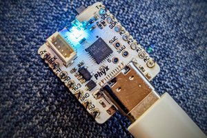
 Wim Van Gool
 Christoph
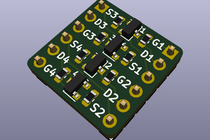
 arturo182