Close
0%
0%

HDD Delta Robot

This is the attempt of building a delta robot using parts from HDD and my parts bin, I'll go as far as I can.

Similar projects worth following
I always saw delta robots very interesting, for that reason I will attempt to build one, but you know what... I honestly know nothig about building delta robots, so this is the best opportunity to learn about delta robots. This project will not be pretty, it's clear that things will go wrong or could be done better, bad decisions will be made, etc, etc, etc... but it doesn't matter that's the natural learning process.

This will be like a very basic "proof of concept" and there will not be a PCB only basic KiCAD schems and perfboards, I decided so because some parts are very old, not recommended for new projects, not common parts, parts like one have on his parts bin for years, also this is for fun and learning and delta robots is something already well documented.

The idea is: use three HDD Actuator arm to move the end effector, controlled by a XMOS startkit. Why HDD actuator arm? curiosity more than anything.

Details about this project are simple (at least on this moment) build a delta robot using:

  • Three or four broken HDD that at least his actuator arm works.
  • My humble Power supplies.
  • Power stage, build from my parts bin.
  • optical isolation, from my parts bin.
  • Microcontroller, also from the same parts bin a never used XMOS startkit.
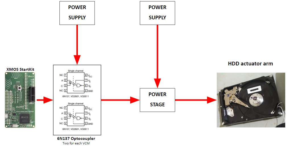
So this is vaguely the diagram that I have on mind for one HDD actuator arm, I dind't define what power stage I will be using because on my parts bin I have different options and I have to analyze what fits better on this, when the power stage and the arrange of power supplies are defined basically will be the same diagram repeated three times.

First I need to work on:

  1. (DONE) Test the four HDD actuator arm voice coil motor (VCM). 
  2. (DONE) Analyze how the power stage will be.
  3. (DONE) Test the 6N137 opto isolators from my parts bin to check if they are still alive.

Then I can move on the next steps:

  1. (DONE) Build the circuit for only one power stage.
  2. (DONE) Build opto isolation for power stage from last point.
  3. (DONE) Make tests (without XMOS).
  4. (DONE) If test are OK then repeat the first three steps two times.
  5. (WORKING ON IT) Do more test (withouth XMOS).
  6. Make "hello world" tutorial for the XMOS startkit.
  7. When I have a decent knowledge start making a simple program to test all the electronics together.
  8. Try to make a decent mechanical structure to mount the three HDD actuator arms.
  9. Try to do the needed mechanical adaptations to each HDD to only left the actuator arm.
  10. Connect all and do more test.
  11. Start serious programming to make that my delta robot do delta robot related stuff...

The 8 and 11 will be what I think more weighty part of all the project, because involve reading and learning about inverse kinematics and many other stuff, so I can know how to put all togetheter to obtain the max movement space, and how to control three arms correctly.

The main goal is: go far as I can.

***NOTE: When this project move to a more advanced state I will do a complete schematic as at this moment isn't suitable make one because even some parts of the project can change a lot...
  • 3 × HDD with working Actuator arm, 10 Ohms VCM
  • 1 × XMOS Startkit
  • 2 × L298HN Interface and IO ICs / Peripheral Drivers and Actuators
  • 6 × 6N137 optocoupler Opto and Fiber Optic Semiconductors and ICs / Optocouplers and Optoisolators
  • 1 × NOTE: as project is going, new components will appear and others will be eliminated of the list...

  • Power stage done.

    Omar09/08/2020 at 05:52 0 comments

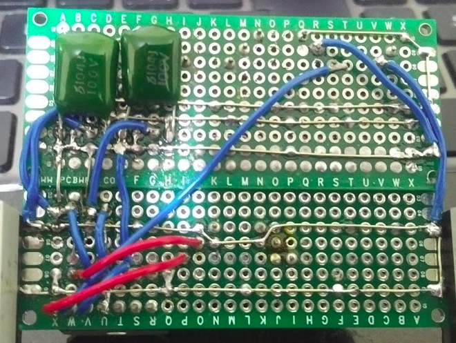
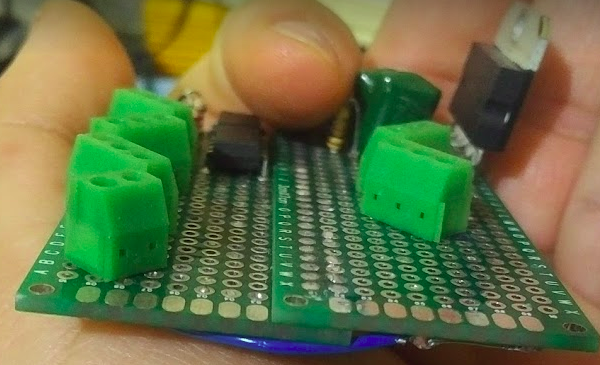
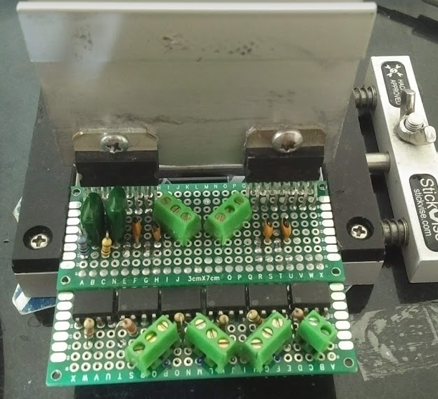
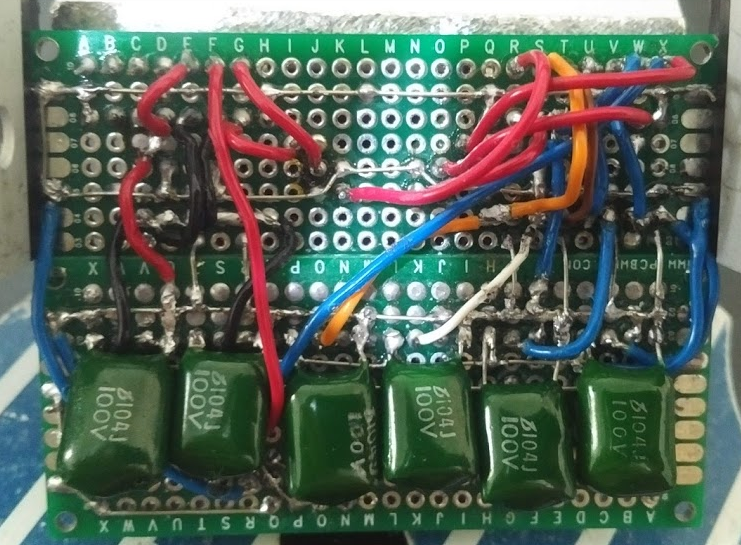
    Hi, finally power stage board is finished, the next step is do more test and maybe make a cable harness for all inputs, outpus and supply.

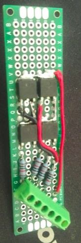
    This is the power stage board (top side):

    Bottom side:

    Isn't the best circuit board that I have done but is functional, at least on brief test, if all other test go well I will make a schematic on KiCAD.


  • problem solved!!!

    Omar08/27/2020 at 06:39 0 comments

    Hi!!, problem solved, the xtime composer have connection problems with DBUS, for this reason xtime composer IDE can't see the messages from udev about the connection/disconnection of the startkit, details about how it was solved will be HERE posted by me with the user name Sodor, it's waiting to be approved by a moderator so it can be published tomorrow. Now I can continue with the power stage board (I almost finish it).

  • More problems

    Omar08/25/2020 at 08:32 0 comments

    My laptop HDD failed, all the info about this project are on google drive so I simply replace the HDD and reinstall Linux, there is the problem, before the failure I have Ubuntu 18.04 LTS with the IDE for XMOS startkit board xTime Composer, all was working fine and the IDE can connect to the startkit without problems, until now....

    My laptop is old, so I installed lubuntu, the problem: there is no USBFS support, because has been deprecated, so I must create rules file for udev in order to mount the board, that is covered in this XMOS document, but after creating the rules for udev on /etc/udev/rules.d/ disconnect and connect the board and doing a service reload to udev the IDE didn't see the XMOS startkit, using lsusb command I can verify detection of the board, I think that maybe the rules file have problems.

    So I need to fix that in order to continue with the XMOS startkit board, may be this take some time due my work and my family and add that I'm not an expert in linux...

  • Thermal related issue

    Omar08/10/2020 at 07:51 0 comments

    Searching on google I found this where the user [Bimpelrekkie] tips about voltage drop on vout of LM350K is due thermal protection, I admit I overstimated that and iniatially I reuse a intel CPU heatsink to mount the LM350K... without the cooling fan powered.... and without thermal grease.....

    Well after powering the cooling fan and using thermal grease for CPU the problem of voltage drop on LM350K was solved (or at least diminished at deprecable levels). So this means that I can continue and finish the power stage board, I only need to solder connections of the second L298H needed for the third VCM.

    For my ToDo list: Learn more about IC thermal managment.

  • First problems

    Omar07/28/2020 at 07:11 0 comments

    Well I know this will happen, is normal and life will be boring without problems, also problems makes success more satisfying when it's achieved. 

    As I advance on the circuit I also do tests, the first test was with only one VCM connected to LM298HM, at that time I don't see any aparent problem, but when I did test with two VCM connected to L298HN I noticed a voltage drop on the ouputs of L298HN to both VCM from 4.5V to 3.23V, I also measured voltage drop at output of the variable power supply (LM350K based), this tell me that voltage drop was on variable power source, so I made a test connecting both VCM in parallel direct to P.S. output, test conditions was:

    • Vin = 19.1V
    • Vout = 5.11V (without load)
    • Vout' = 3.51V (with two VCM connected)
    • RL = 5 Ohms (both VCM are 10 Ohms connected on parallel)
    • IL = 0.690 A  (measured)

    If you see there is a voltage drop of 1.6V on Vout when load is connected to P.S. I need to check the datasheet to find what is wrong here (or if this is normal). Also there is a voltage drop too if I use only one VCM but is low enough to overlooked it on first tests, so if I connect three VCM then the voltage drop will be more than 1.6V (however I don't tested it).

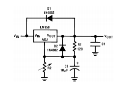
    This is the used circuit (from TI datasheet):


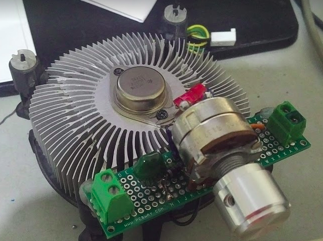
    And this is the implemented circuit:

    D1 and D2 are 1N4006, C1 100nF, R2 is a 25k pot.

    I don't think this problem is thermal related because LM350K use a large heatsink and the changes on Vout are fast as the change of load. Well I will start here the analysis to find the possible problem, wish me success.

  • The sad MOSFET H-Bridge

    Omar07/08/2020 at 06:45 0 comments

    The last time I said that I changed my mind about power stage, this is why... I used 4 MOSFET D-PAK STD22NM20N, a spare perfboard from those that PCBway always give away and other basic components.

    Then I realized that will be difficult to put a heat sink on this and surely I will need a heat sink for each bridge... but while I was thinking about it I remembered that I have some L298HN on my parts bin. Those IC can control up to two direct current motors on both directions each one, two of them  can control three HDD actuator arm, at 15 pin each IC I can use prefboard without problems also the horizontal package ease the mount of a heat sink even if I can place both IC appropriately both can share the same heat sink.

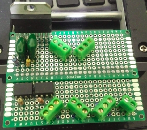
    First I build only the minimum to control one VCM from opto isolators to L298HN and do some test, and this is the result.

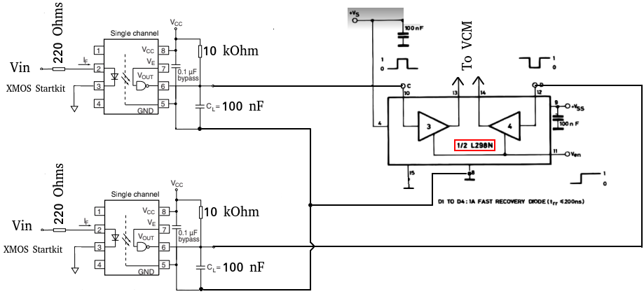
    If you see I soldered two perfboards togheter, in the end the area was much smaller than having used  H-Bridge option, Optocouplers are 6N137. At this point the circuit is incomplete and has this schematic:

    OK first I need to say that I've been a little lazy on this schematic, I used images from the datasheet of both IC I trust it won't cause much problem... So the schematic in part isn't the implemented circuit, the L298HN on the schematic show the full bridge composed of amplifiers 3 and 4, the implemented circuit used 1 and 2, the only differences are on pin used on the L298HN to use the amplifiers 1 and 2 (inputs and ouputs) check the datasheet for more details, also there is no sensing resistor on implemented circuit.

    I test the circuit with this conditions:

    • Optocouplers Vin 3.3V
    • Optocouplers Vcc 5V
    • L298HN power suppy Vs 7V
    • L298HN Logic supply Vss 5V
    • HDD VCM connected on output of amplifiers 1 and 2

    Test went well, and the HDD actuator arm move on both direction as Vin was a logic high on one optocoupler and low on the other and viceversa.

    I have to say that just before I start the circuit build I tested all the 6N137 optocouplers on a breadboard and six of seven work, six is the number that I need, I don't have more 6N137 I must be very carefully to not damage any.

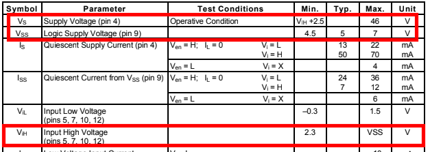
    Now why 7V for L298HN Vs? the reason is that as I stated on past logs I want to supply the VCM with 4.5V - 5V, so the datasheet for L298HN says this:

    and this:

    The LN298HN has it's dual H-bridge based on BJT, if I want Vl = 4.5V to 5V then I need to apply a Vs that by subtracting the Vce drop from on transistors susch that Vl will be on the range, then from datasheet Vcesat = 1.8V to 3.2 at 1A current, on my case are 450mA to 500mA, so with Vs = 7V then Vl = 5.2V to 3.8V if Vl is above or under the range of 4.5V to 5V then I simply adjust Vs. 

    With the first try (Vs = 7V) the measured Vl on the output with VCM connected gave me 4.5 Volts, it work even with Vs under the minimum, datasheet says Vsmin = Vih +2.5V and with Vih = 5V  Vsmin = 7.5V... but it works excellent!!! Sorry there is no photo of this :¬(,  now I can continue...

    In the next update I will show the power stage circuit completed and tested (I hope).

  • Power Stage

    Omar07/06/2020 at 07:15 0 comments

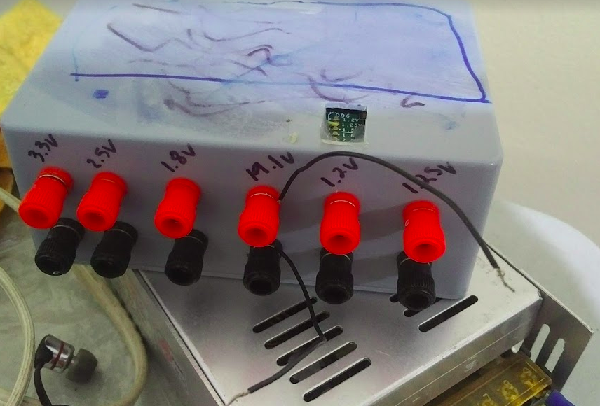
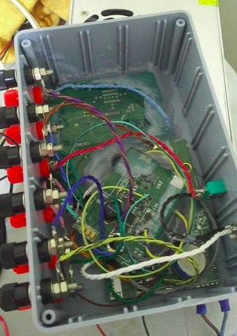
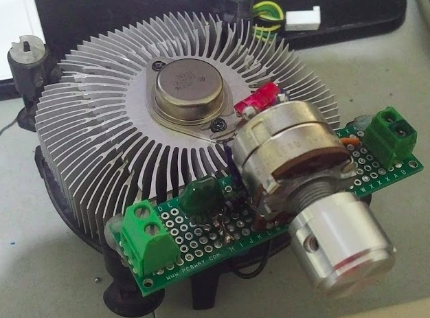
    The first option on mind was to build an H-bridge with N-channel MOSFETS (because I have a bunch of D-PAK STD22NM20N on my parts bin) for that I need to use a MOSFET driver that also have on my parts bin, one for each H-bridge, so three will be needed, each one of 20 pins a PCB was the best option for this, desinged on KiCAD and use PCBway.... that killed the idea... first I don't want to make a PCB for this, I want to use what I have on my house and parts bin, use prefboards??... the ones I have are too small... the second option was don't use the driver IC and drive the MOSFETs directly using opto isolators, but I will need two power supplies at different voltage levels, one for low side MOSFETS with at least more than 5Vcd to drive them and other at 9.5 to 10 volts for high side MOSFETS, the problem: I have only two power supplies, both are fixed voltage, one at 5 volts and the other have multiple fixed voltage levels, (3.3v, 2.5v, 1.8v, 1.2v and 19.1v)... the solution was a simple one: build a variable power supply based on one of LM350K from my parts bin and use the 19.1v for Vin needed.

    On top the multiple fixed voltage power source on bottom the 5V fixed voltage PS.

    These are the guts of my multiple fixed voltage PS, made with love, the PS sections from a motorola microwave ODU, hot glue and a hacksaw.

    and this is my new humble variable PS based on LM350K


    The next step was to make the H-Bridge with the D-PAK MOSFET, but then again another change of mind happened, this time was too late... but that history will be for the next log.

  • HDD test

    Omar07/05/2020 at 20:44 0 comments

    I have dissablembled 4 broken seagate HDD, retired the logic board and cover top, I noticed that not all HDD are the same model because not all have the same number of plates inside, I thought that all 4 disk would be the same model because all looks identilcal and none have its external labels.

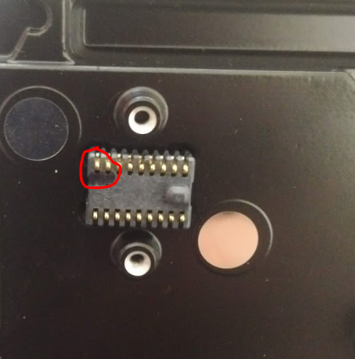
    Whatever looking the related circuitry of the VCM the coil connections are exposed to pins used to connect to logic board, so I use a multimeter and search for a low resistante value.

    On these pins I have 10 Ohms value, I applied 5V and the actuator arm moved fast, reversed the polatrity and the actuator arm move to opposite direction, the same test on the other 3 HDD revealed that despite they are different models all use the same two pins and read 10 Ohms value.

    Starting from here I think that a operating voltage of 4.5 to 5 Vcd for each VCM is good enough for this experiment.

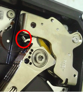
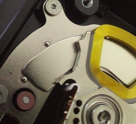
    Is needed to remove a little piece of metal near the VCM, is used to maintain the actuator arm on rest position when is not in use, this because it doesn't allow a free movement of the HDD arm because when the arm is on certain position the magnets atract it to rest position.

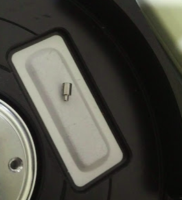
    Using pliers I carefully remove the metal post...

    Now the HDD actuator arm can move freely on his restricted range.

View all 8 project logs

Enjoy this project?

Share

Discussions

Martin wrote 07/28/2020 at 09:40 point

I don't see any use in the opto isolators. You have both GNDs connected - which is a good thing anyway. It's better to have a solid GND and not different ones. You somehow use them as level converters which is unnecessary anyway. You even marked the V_ih in the datasheet excerpt in red: min. 2,3V. So you can control it with 3,3V CMOS logic signals.

  Are you sure? yes | no

Omar wrote 07/29/2020 at 01:42 point

Ohh yes yes... this is the problem of being lazy... my fault, as I stated on the log I used screen captures from opto datasheet (among others) and I overlooked that connection between input GND and output GND, thanks for pointing that I will delete it. Yes you are correct the minimum logic high input of the L298HN is 2.3V so it will be happy to work with XMOS startkit 3.3V logic, but I only have one XMOS startkit, for that reason all inputs on power stage are opto isolated and input GND is separated from output GND to prevent some possible damage (again my fault, the schematic is not equal to implemented version), but Vs and Vss of L298HN have same GND.

  Are you sure? yes | no

Martin wrote 07/29/2020 at 09:07 point

Of course it is good, to think about protection of sensitive microcontroller ports from bad things out of the power part. Luckily there is normally an easy and cheap solution for this problem: The simple resistor.

Microcontroller ports normally have diodes for ESD and overvoltage protection which can carry a few mA of current. If your signals are not too fast, it is easy to calculate a series resistor for the signal that limits the current to a safe value even if your power stage burns down and feeds its operating voltage backwards.

If your µC does not allow this small currents into its outputs (this is also possible), I would use something like 74HC244 as a buffer and have a few kOhms in series.

Separated power supplies are extra effort anyway, so there is a regulator to make the µC supply from the main (battery) voltage and the GNDs are of course the same.

Btw.: I have a relay board from Aliexpress (similar to Adafruit or sparkfun stuff) which has opto's and advertises them. And they are completely useless as the GNDs are tied together. So yours would not have been the first design, I know, where this mistake was done. Luckily there is galvanic isolation to the mains voltage side (230V) by the relays themselves. But instead of the opto a simple transistor would have been enough.

I use (optical) isolation when I have e.g. separated parts of a system which have to communicate but have separated power supplies and a long distance between. For example several DMX connected devices, each with it's own PSU. Then it makes sense to design the DMX interface with opto's.

  Are you sure? yes | no

Omar wrote 07/30/2020 at 15:40 point

Thanks Martin I will get your advice, if this project advances more than this functional prototype  this will be one of the many points of improvement.

  Are you sure? yes | no

Similar Projects

Does this project spark your interest?

Become a member to follow this project and never miss any updates