 tuenhi.n2012
-
1SOLDERING LED CUBE MODULE
We can refer to lots of projects related on how to build a led cube.
You should make a wooden cube template with 16 holes, diameter 10mm and led tester with battery to check before and after soldering your LED.
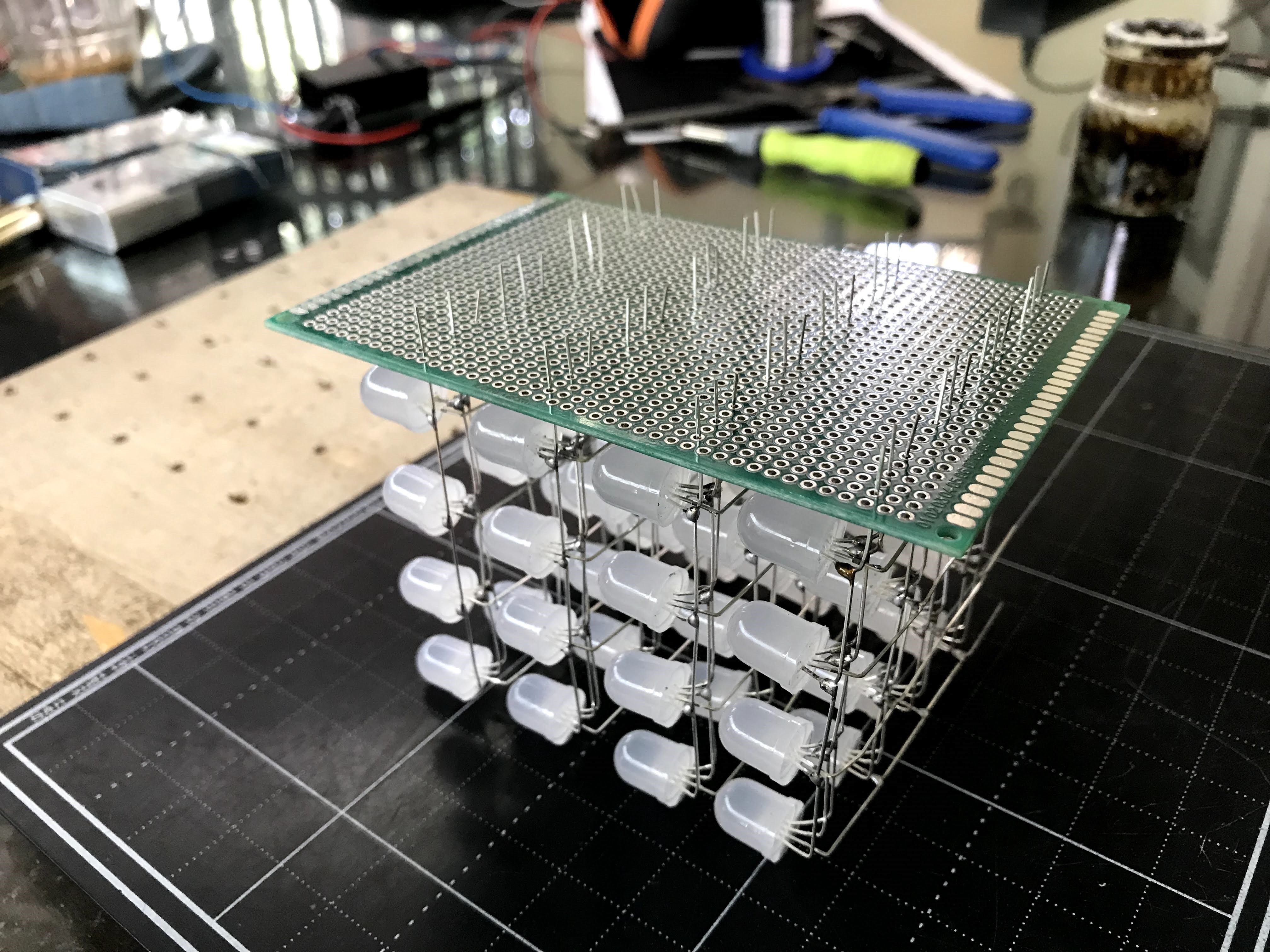
After soldering 04 planes of led cube, I arranged and assembled them into the Prototype PCB 8X12CM.
![]()
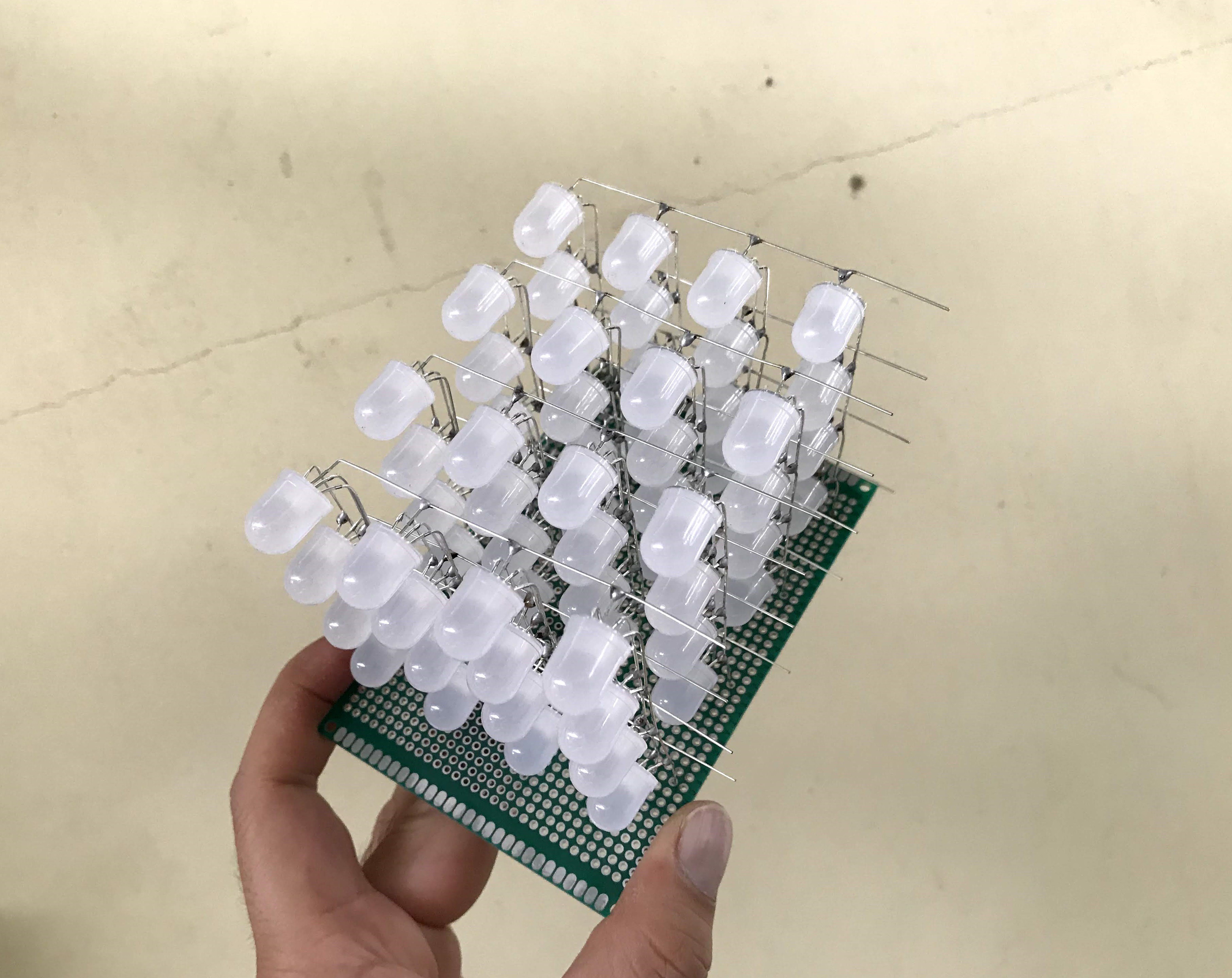
I aligned them neatly and symmetrically then soldered them to the Prototype PCB.
![]()
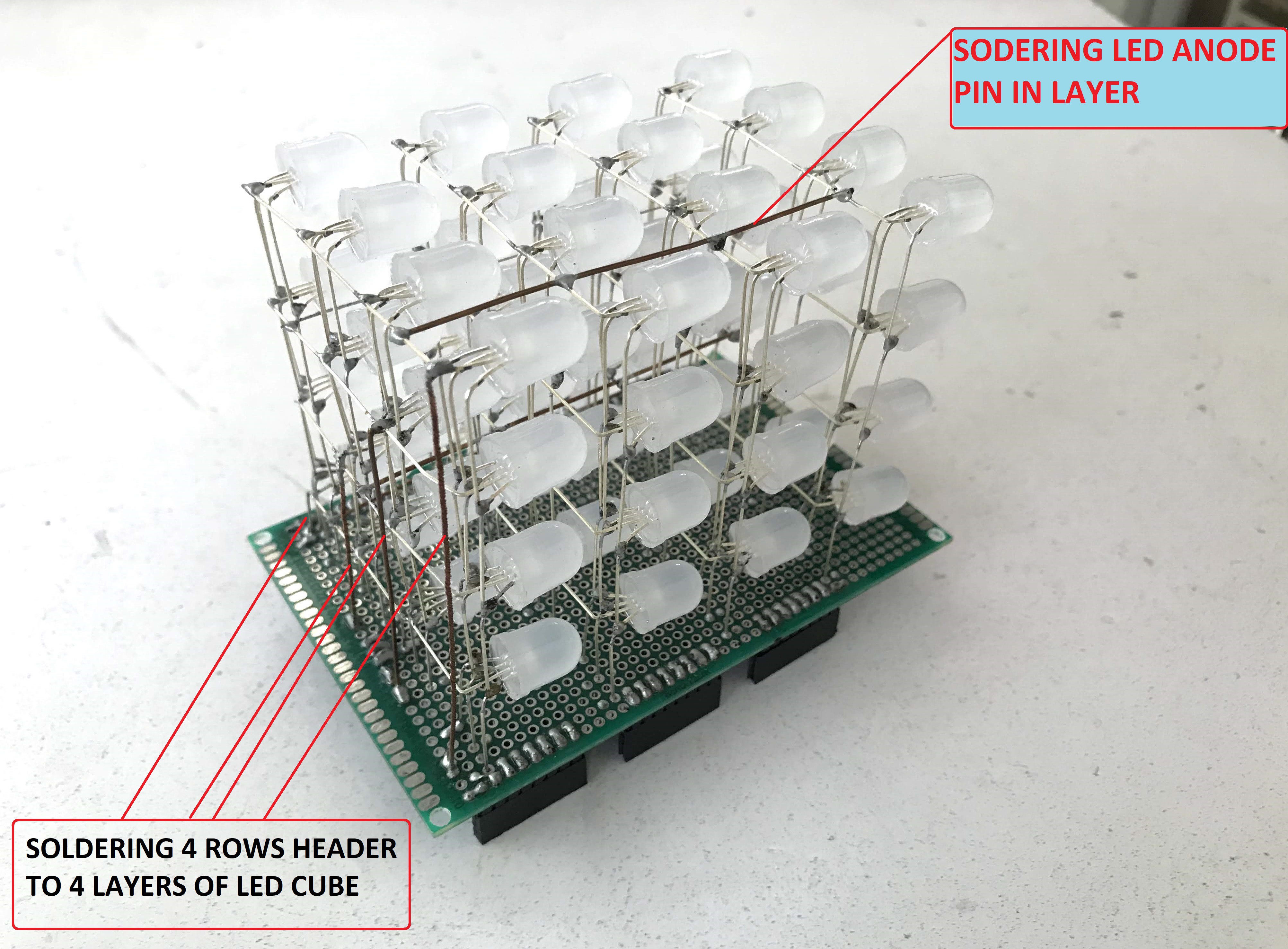
On top of led cube, I soldered 16pcs x RGB LED ANODE PINS in same layer together by copper wires. We have totally 4 layers and they are connected to a 4 pin female header at bottom. Later they will be plugged on control board at this header.
![]()
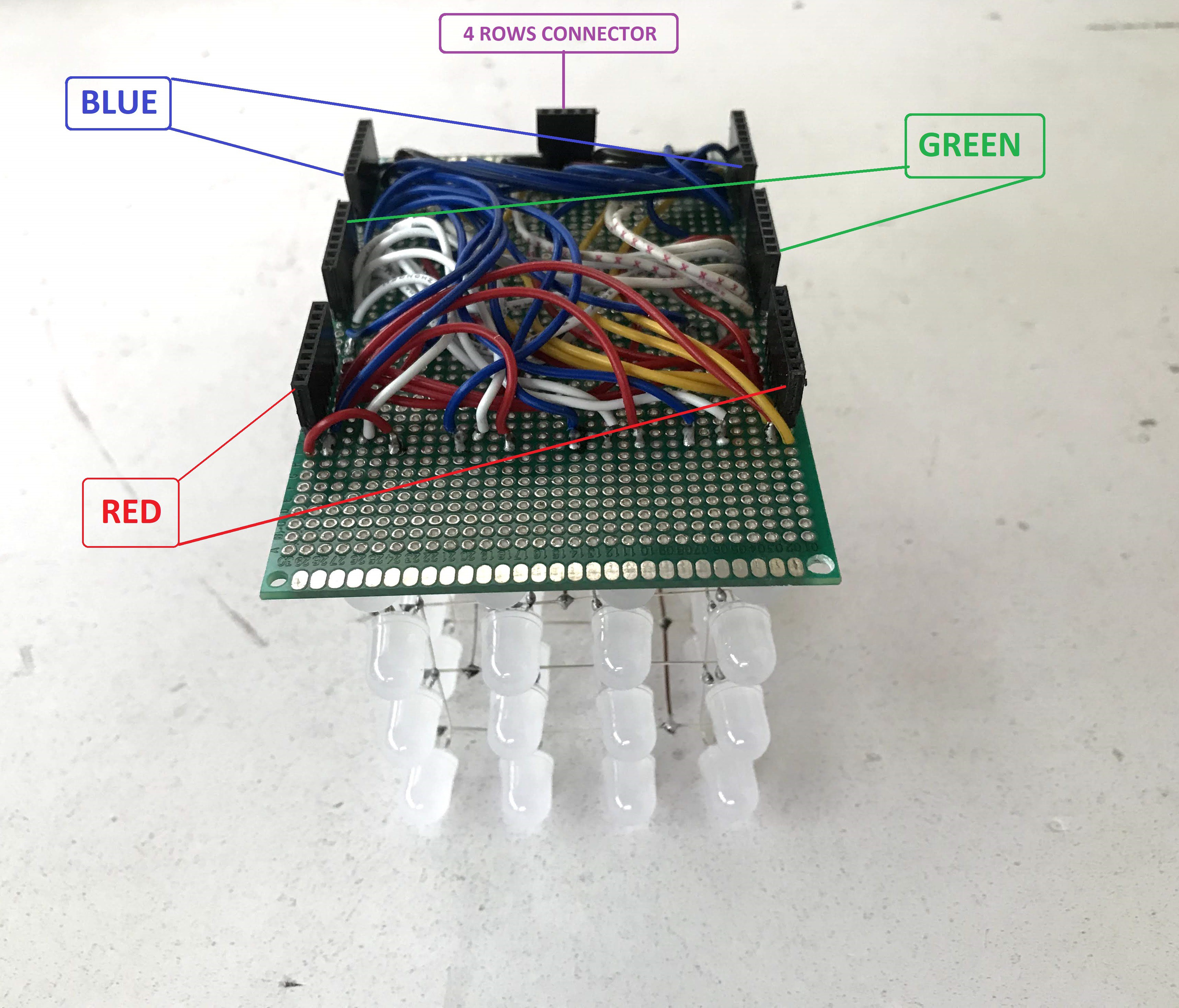
At bottom of led cube, I soldered LED CATHODES PIN to 6pcs x 8P-female headers in color groups: RED, GREEN & BLUE. As explained in previous step, because each layer has 16 RGB LEDs, so we need to use 2pcs x TPIC6B595N to control each color.
![]()
RGB Led cube 4x4x4 module is DONE!!!
-
2SOLDERING CONTROL MODULE
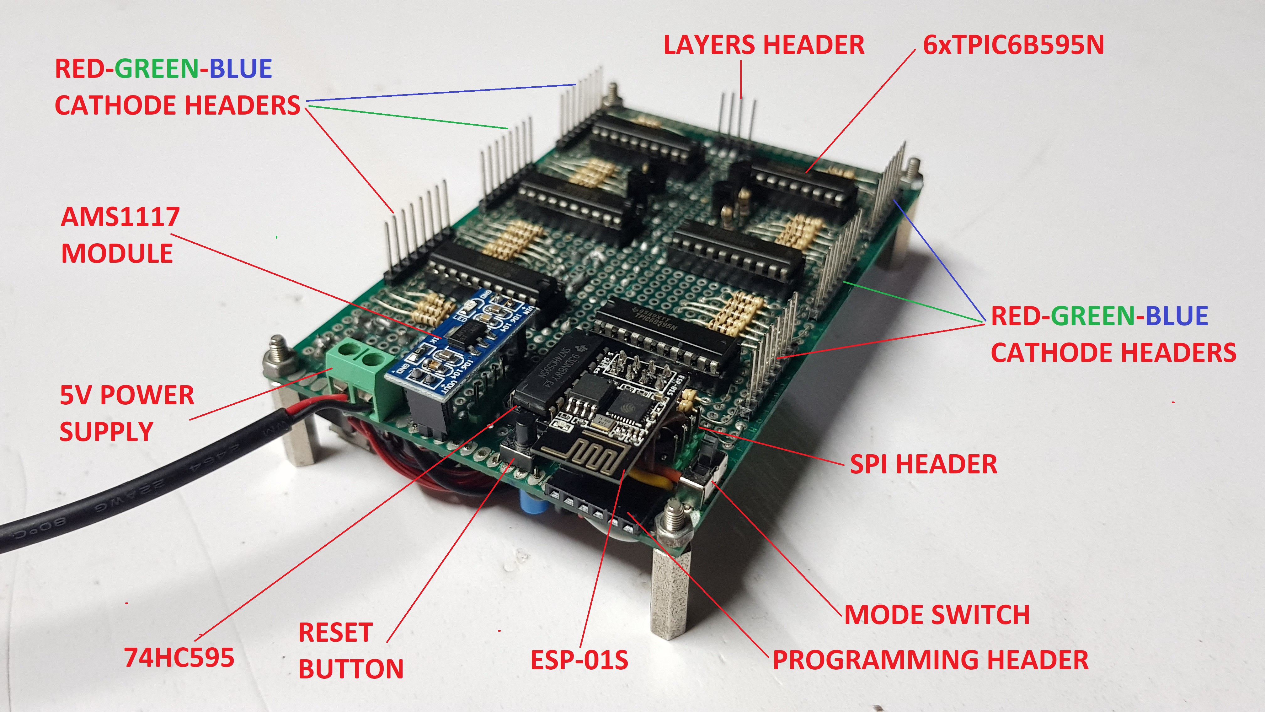
I used a remaining prototype PCB 8X12CM to solder the control circuit following the schematic on previous step. Note that in order for led cube module and control module to be matched together perfectly, firstly we have to align & solder all male headers on control module following female headers of led cube.
![]()
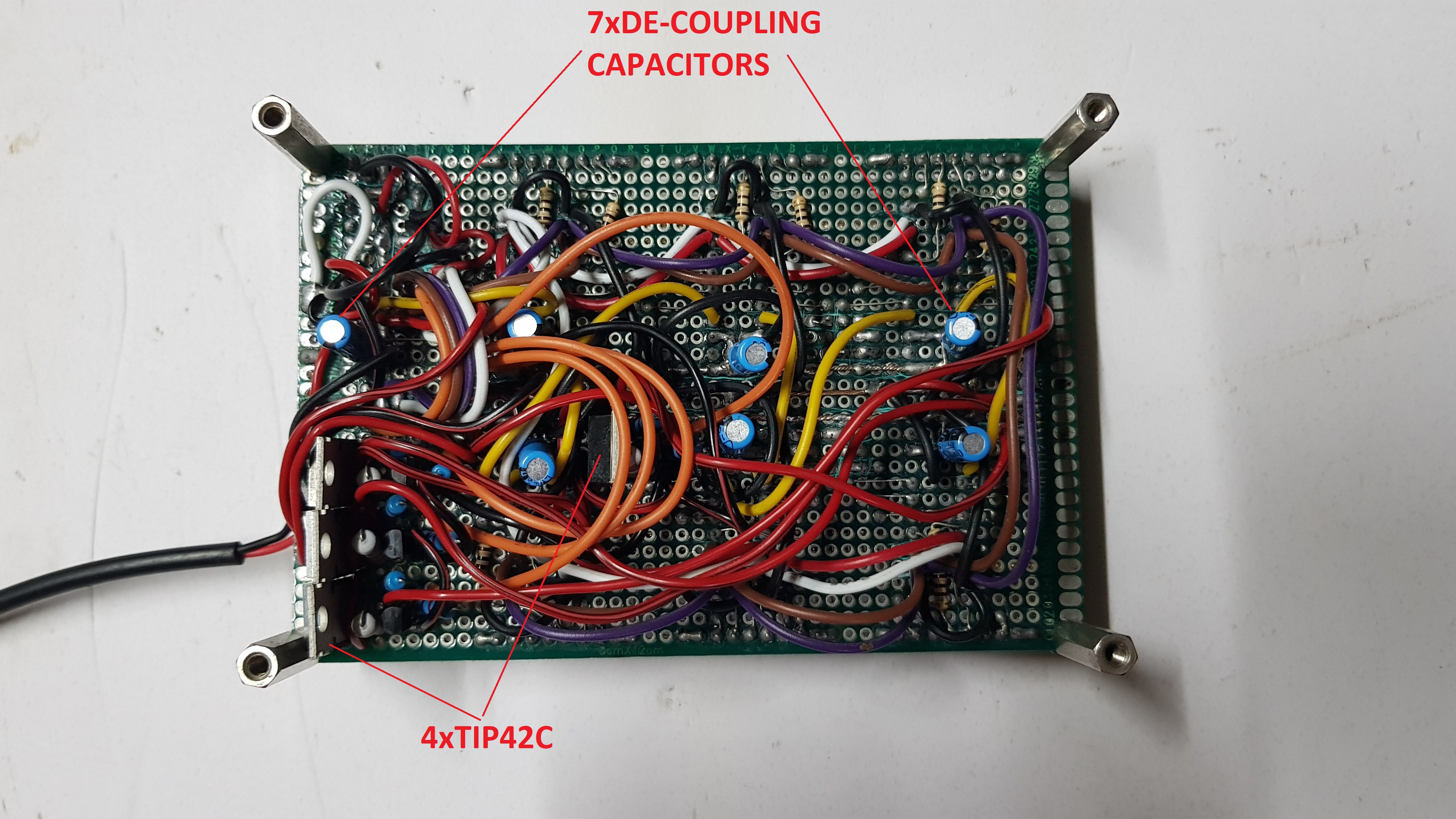
Picture below is bottom side of control module. I soldered all de-coupling capacitors and high power transistors TIP42C at bottom.
![]()
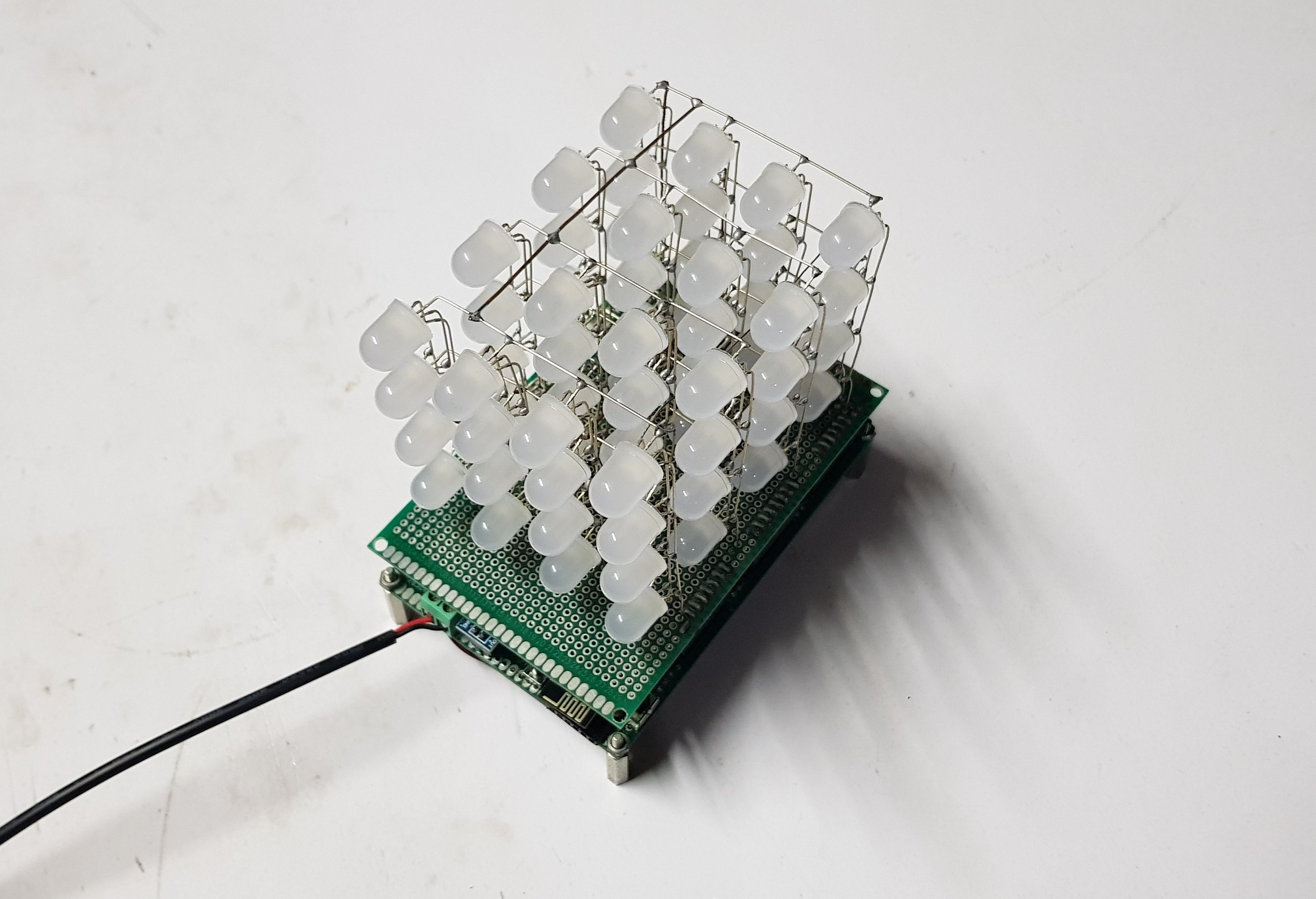
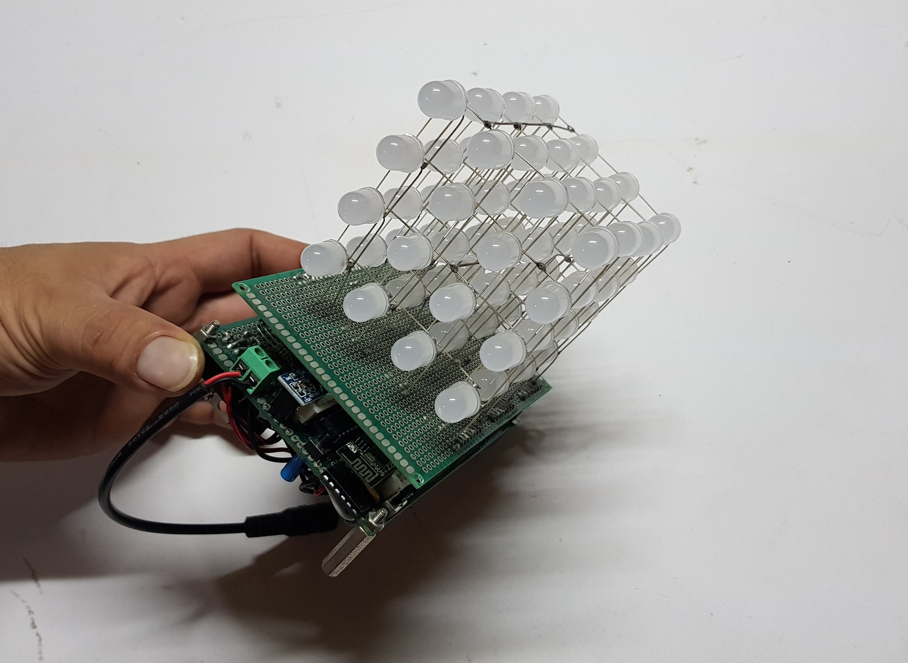
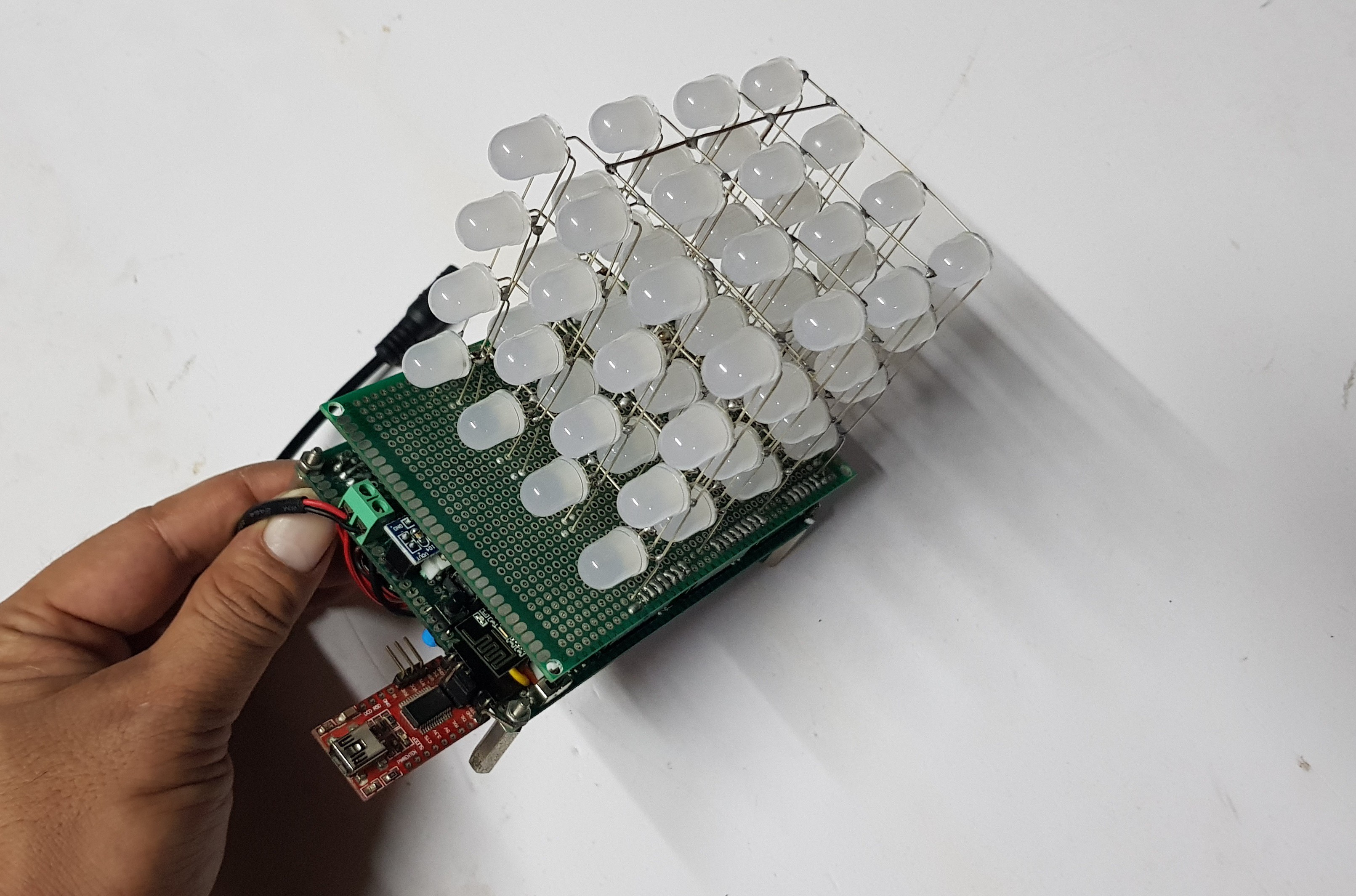
Finally I plugged led cube module on top of control module.
![]()
![]()
All soldering works were done and we go to next step for programming!!!
-
3PROGRAMMING
In my program, ESP-01S ESP8266 is used as a stand-alone device to control a RGB led cube 4x4x4. The project code is available at my GitHub.
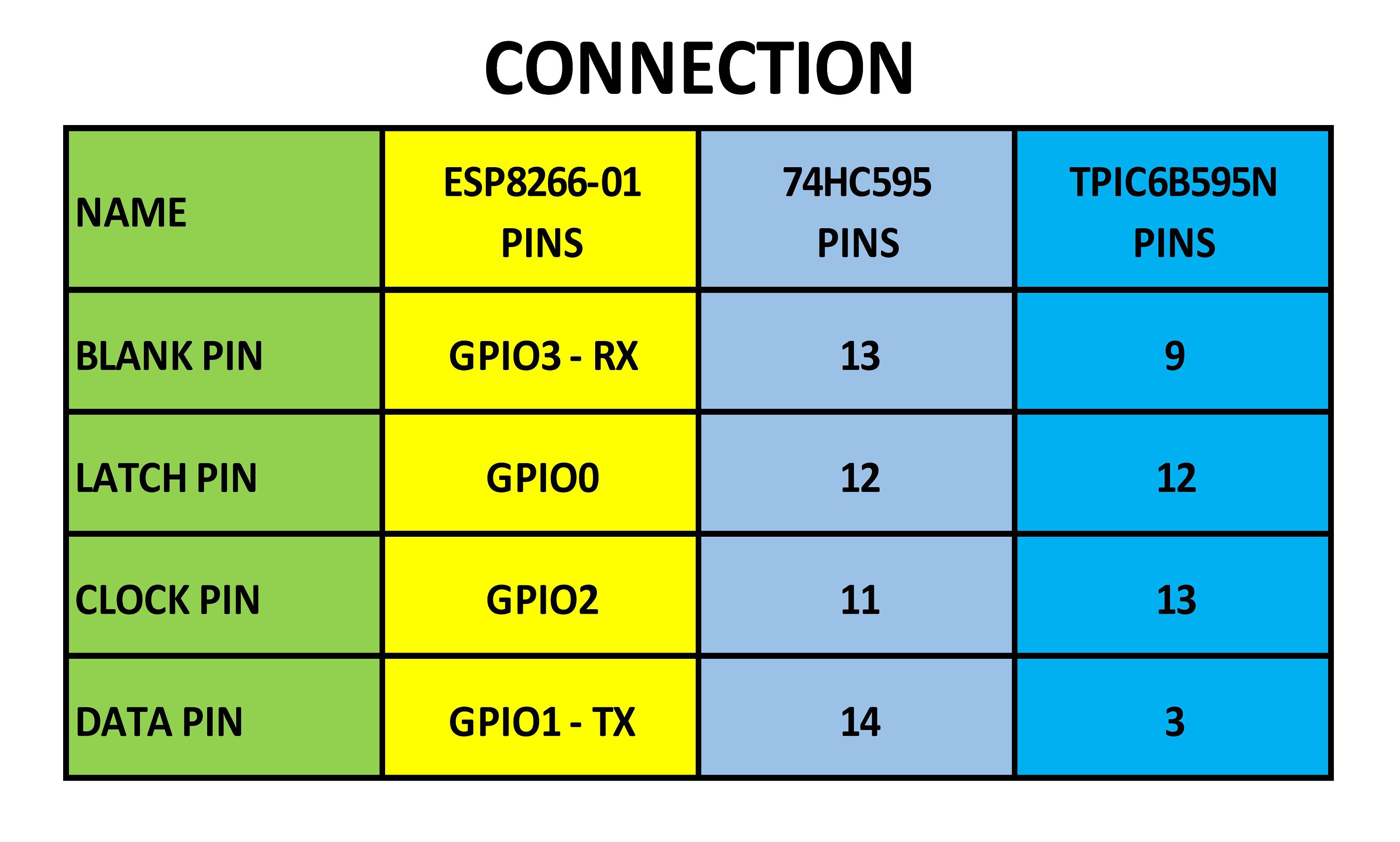
CONNECTION
The ESP-01S ESP8266, 74HC595 & TPIC6B595N are connected together as follows:![]()
LED CUBE CONTROL
For layer scanning (anodes), because my led cube module has 4 layers, so we need to shift out 1 byte to 74HC595 with order from 0 ~ 3, as following anode array below.byte anode[4]= {B00001000, B00000100, B00000010, B00000001};I referenced to original shiftOut() function in file "core_esp8266_wiring_shift.cpp" to create for my own SPI function. You can search this file on your computer or check at this LINK.
void __attribute__((optimize("O0"))) DIY_SPI(uint8_t DATA)
{
    uint8_t i;
    uint8_t val;
    for (i = 0; i<8; i++)
    {
      digitalWrite(DATA_Pin, !!(DATA & (1 << (7 - i))));
      digitalWrite(CLOCK_Pin,HIGH);
      digitalWrite(CLOCK_Pin,LOW);
    }
}
In this project, I used Timer 1 in ESP-01S ESP8266 and a callback routine to implement B.A.M process.
timer1_isr_init();
timer1_attachInterrupt(timer1_ISR);
timer1_enable(TIM_DIV16, TIM_EDGE, TIM_SINGLE);
timer1_write(60);
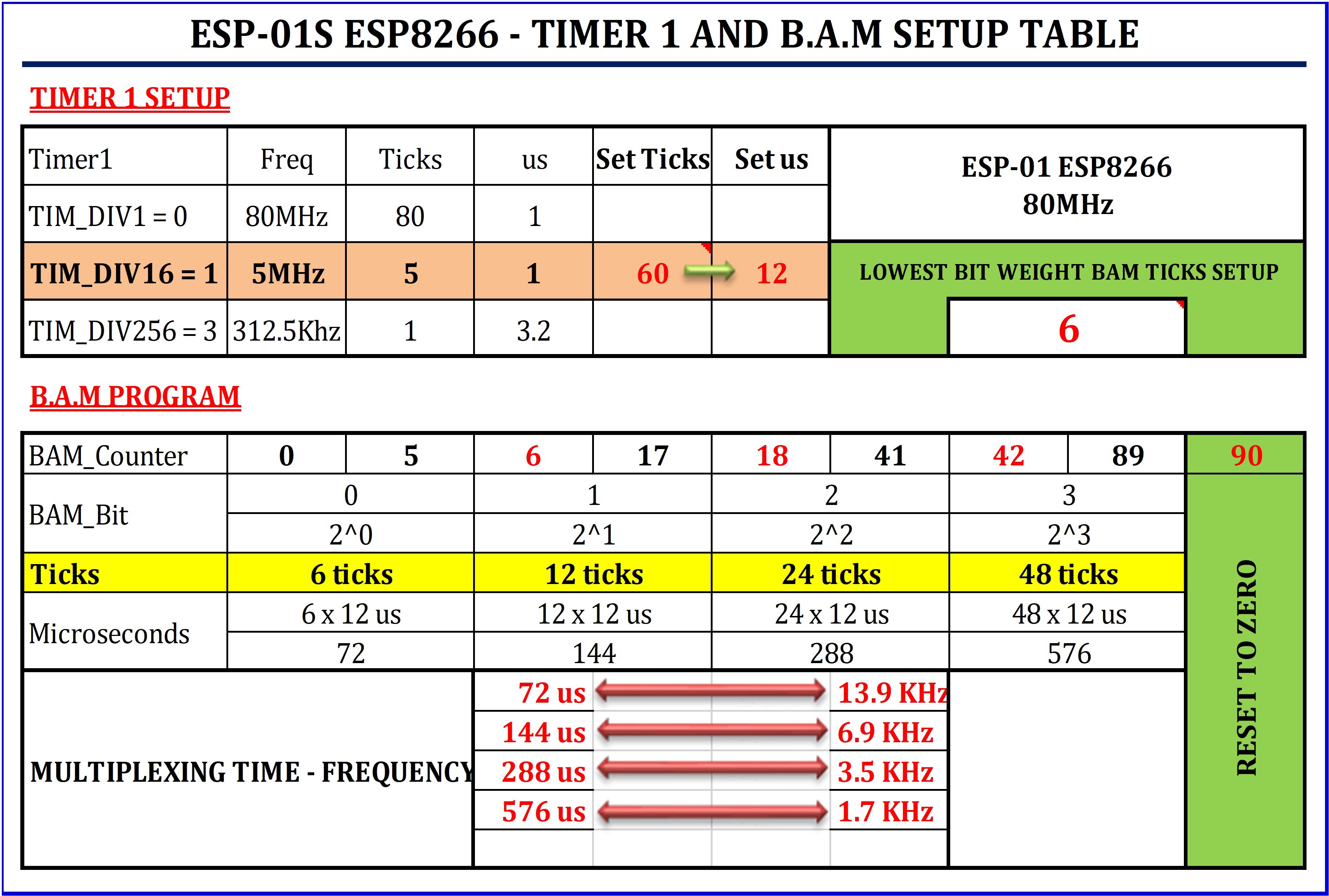
The table below describes the Timer 1 and B.A.M settings as well as their relationship. With this setup, our timer clock runs at 5MHz (80MHz/16=5MHz) or 1/5MHz = 0.2us. When we set timer1_write (60), this means the interrupt will be called every Tick = 60 x 0.2us = 12us and 4 bit B.A.M process need 6 Ticks x 12us = 72us to set the "Least Significant Bit of BAM_Bit" to "ON" or "OFF", which gives a multiplex frequency of about 13.9kHz.
![]()
Main attach interrupt service routine code:
void ICACHE_RAM_ATTR timer1_ISR(void)
{
digitalWrite(BLANK_Pin, HIGH);

if(BAM_Counter==6)
BAM_Bit++;
else
if(BAM_Counter==18)
BAM_Bit++;
else
if(BAM_Counter==42)
BAM_Bit++;
BAM_Counter++;
switch (BAM_Bit)
{
case 0:
       //Blue
        DIY_SPI(blue[0][level + 1]);
        DIY_SPI(blue[0][level]);
      //Green
        DIY_SPI(green[0][level + 1]);
        DIY_SPI(green[0][level]);
      //Red
        DIY_SPI(red[0][level + 1]);
        DIY_SPI(red[0][level]);
      break;
    case 1:
      //Blue
        DIY_SPI(blue[1][level + 1]);
        DIY_SPI(blue[1][level]);
      //Green
        DIY_SPI(green[1][level + 1]);
        DIY_SPI(green[1][level]);
      //Red
        DIY_SPI(red[1][level + 1]);
        DIY_SPI(red[1][level]);
      break;
    case 2:
      //Blue
        DIY_SPI(blue[2][level + 1]);
        DIY_SPI(blue[2][level]);
       //Green
        DIY_SPI(green[2][level + 1]);
        DIY_SPI(green[2][level]);
      //Red
        DIY_SPI(red[2][level + 1]);
        DIY_SPI(red[2][level]);

      break;
    case 3:
      //Blue
        DIY_SPI(blue[3][level + 1]);
        DIY_SPI(blue[3][level]);
      //Green
        DIY_SPI(green[3][level + 1]);
        DIY_SPI(green[3][level]);
      //Red
        DIY_SPI(red[3][level + 1]);
        DIY_SPI(red[3][level]);
  if(BAM_Counter==90)
    {
      BAM_Counter=0;
      BAM_Bit=0;
    }
  break;
}

DIY_SPI(anode[anodeLevel]);

digitalWrite(LATCH_Pin, HIGH);
digitalWrite(LATCH_Pin, LOW);
digitalWrite(BLANK_Pin, LOW);

anodeLevel++;
level = anodeLevel<<1;
if(anodeLevel == 4) anodeLevel=0;
if(level==8) level=0;

//pinMode(BLANK_Pin, OUTPUT);
timer1_write(60);
}
Below code is used to set a LED based on its coordinates and color.
void LED(int CZ, int CY, int CX, int CR, int CG, int CB) { CR = constrain(CR, 0, (1 << BAM_RESOLUTION) - 1); CG = constrain(CG, 0, (1 << BAM_RESOLUTION) - 1); CB = constrain(CB, 0, (1 << BAM_RESOLUTION) - 1); int WhichByte = int(((CZ<<4) + (CY<<2) + CX) >> 3); int WhichBit = (((CZ<<4) + (CY<<2) + CX) - (WhichByte << 3)); if (inrange(CZ,CY,CX)) { for (byte I = 0; I < BAM_RESOLUTION; I++) { //*** RED *** bitWrite(red[I][WhichByte], WhichBit, bitRead(CR, I)); //*** GREEN *** bitWrite(green[I][WhichByte], WhichBit, bitRead(CG, I)); //*** BLUE *** bitWrite(blue[I][WhichByte], WhichBit, bitRead(CB, I)); } } } -
4UPLOADING PROGRAM
Uploading the program by FTDI module and take notes:
- In my program, you can see that GPIO0 of ESP-01 connect to LATCH PIN of 74HC595 & TPIC6B595N for latch function and it is set HIGH and LOW (GND) during this process. As far as my reference, there is no information about how long an interval we should set GPIO0 between the HIGH and LOW level to put ESP-01 into programming mode, but with my hardware and program code it works perfectly without any errors or interruptions.
- When I want to upload the program, I can plug FTDI programmer into programming header, remove SPI header, switch S2 (mode switch) to GND position and ensure the external power is supplied to ESP-01.
- After uploading, switching slide switch to NORMAL operation and push RESET button.
![]()
ESP-01 CONTROL RGB LED CUBE 4x4x4
ESP-01 ESP8266 can be used as a stand-alone device to control a RGB led cube 4x4x4.
Discussions
Become a Hackaday.io Member
Create an account to leave a comment. Already have an account? Log In.