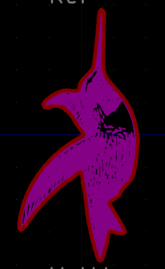
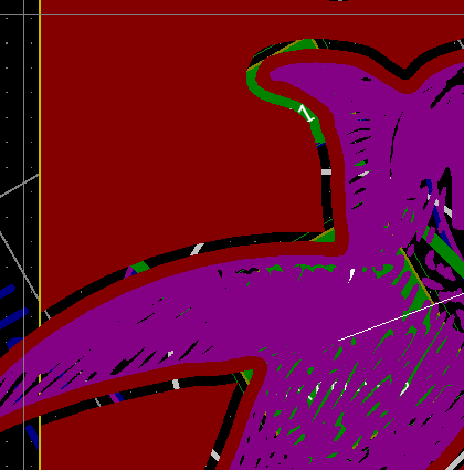
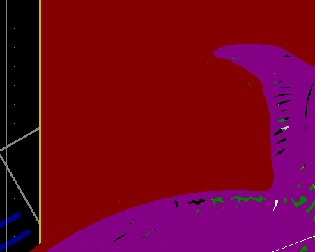
Decided to just jump right onto a repeat of the Hummingbird earrings fixing some of the problems described in the previous log. And a complete shock to no-one, it turned out to be more fiddly than expected. The big change I wanted for this was to have copper on the entire front side, which a mask of the bird cut out. I got close a couple times, except the pour wouldn't come all the way up to the mask. To start I used the svg2shenzen plugin for Inkscape to create the footprint below. It's the same solder mask as before but I've added a F.Cu border all the way around.
 Once in KiCAD this had the annoying problem of following the clearance rules. But I figured out the trick is to change the Board Setup and reduce the default net to have 0mm clearance.
 The more proper way (I think) would be to add a NetClass to the pour, but I couldn't remember how to do that and what I have mostly worked. The one issue I did have was because I overwrote the default class, some of the LED pins needed local clearance set have to 0.2mm. This will get explored further.
Next up I will hopefully do my next Internal Edge Lit board, it's been a bit of a pain to get it how I want, I really should just go with a 4-layer board and be done with it. We'll see next Monday what happens.
 morgan
Discussions
Become a Hackaday.io Member
Create an account to leave a comment. Already have an account? Log In.
What about just double-clicking the zone and setting clearance to zero on that one pour?
Are you sure? yes | no
https://i.imgur.com/AvEVvTW.png
Are you sure? yes | no
But now add something with a pad, or another pour. That works fine for the board edge but doesn't seem to behave the same for copper on copper.
Are you sure? yes | no
Doesn't the Kicad bitmap to component converter allow you to do something like make the copper negative (just make in silk or mask layer and then replace the layer name with F.Cu in a text editor)? Then maybe make a custom pad in the footprint editor to give the copper pour something to connect to.
Are you sure? yes | no
Maybe? It's probably time to revisit that tool but last time I worked with it I recall having a bad time. Maybe things have changed but then, between svg2shenzen, kicadStepUp and some more practice I'll get this process down.
Are you sure? yes | no