-
Problems
07/11/2020 at 22:31 • 0 commentsHere I want so show you two typical problems when etching PCBs and possible ways to solve the situation.
Here is a PCB I made where nothing went right.
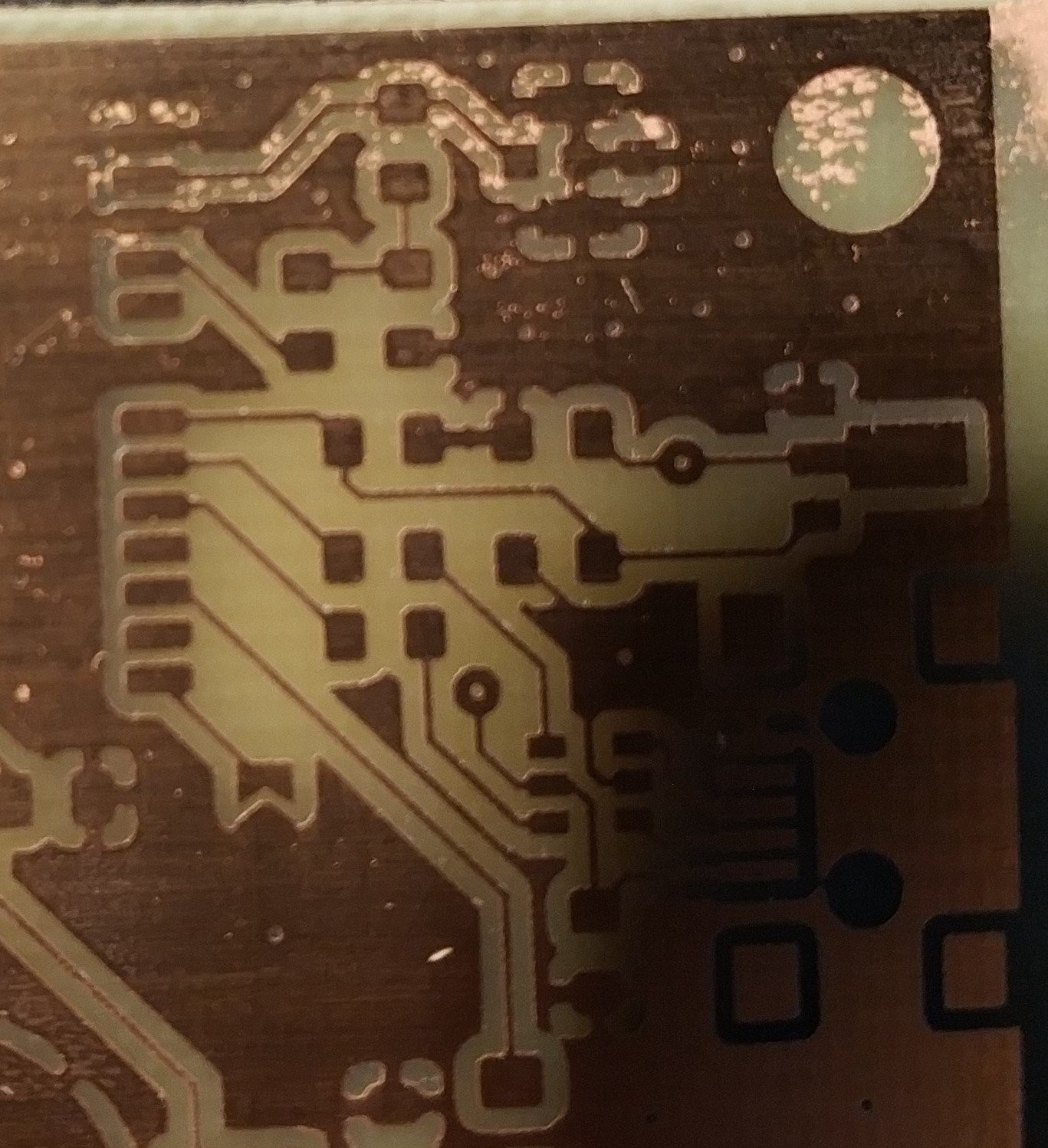
First a small area of the PCB took very long to clear of all the copper. I eventually stopped the etching process to not overetch the other areas (sorry for the blurry photo).
![]()
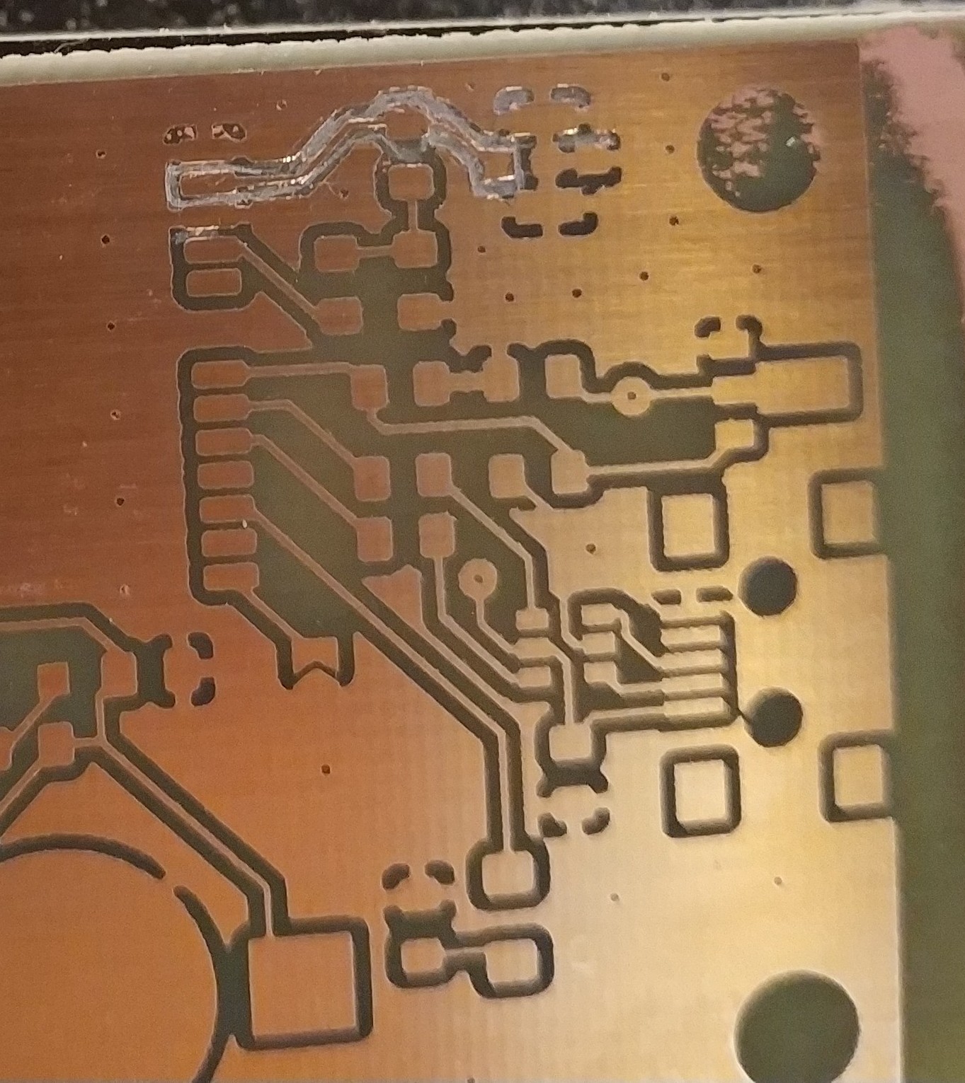
A easy fix for this problem is to scratch away the residual copper in between the traces with a pointy tweezer or knife etc. The result does not look that nice anymore but there was no longer a short from the groundplane to the trace.
![]()
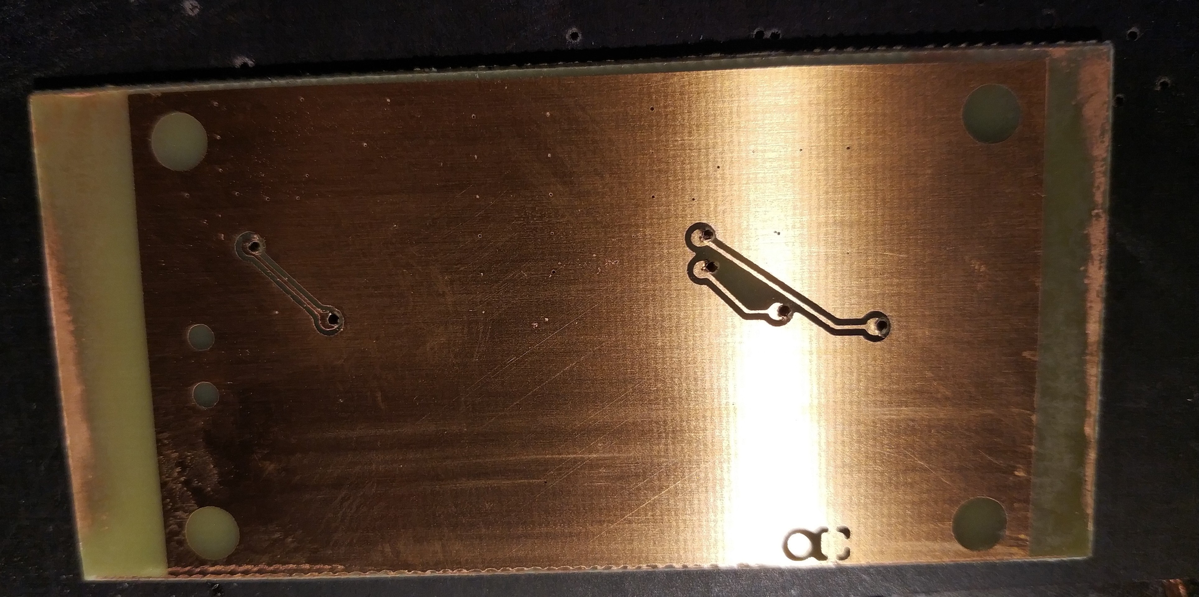
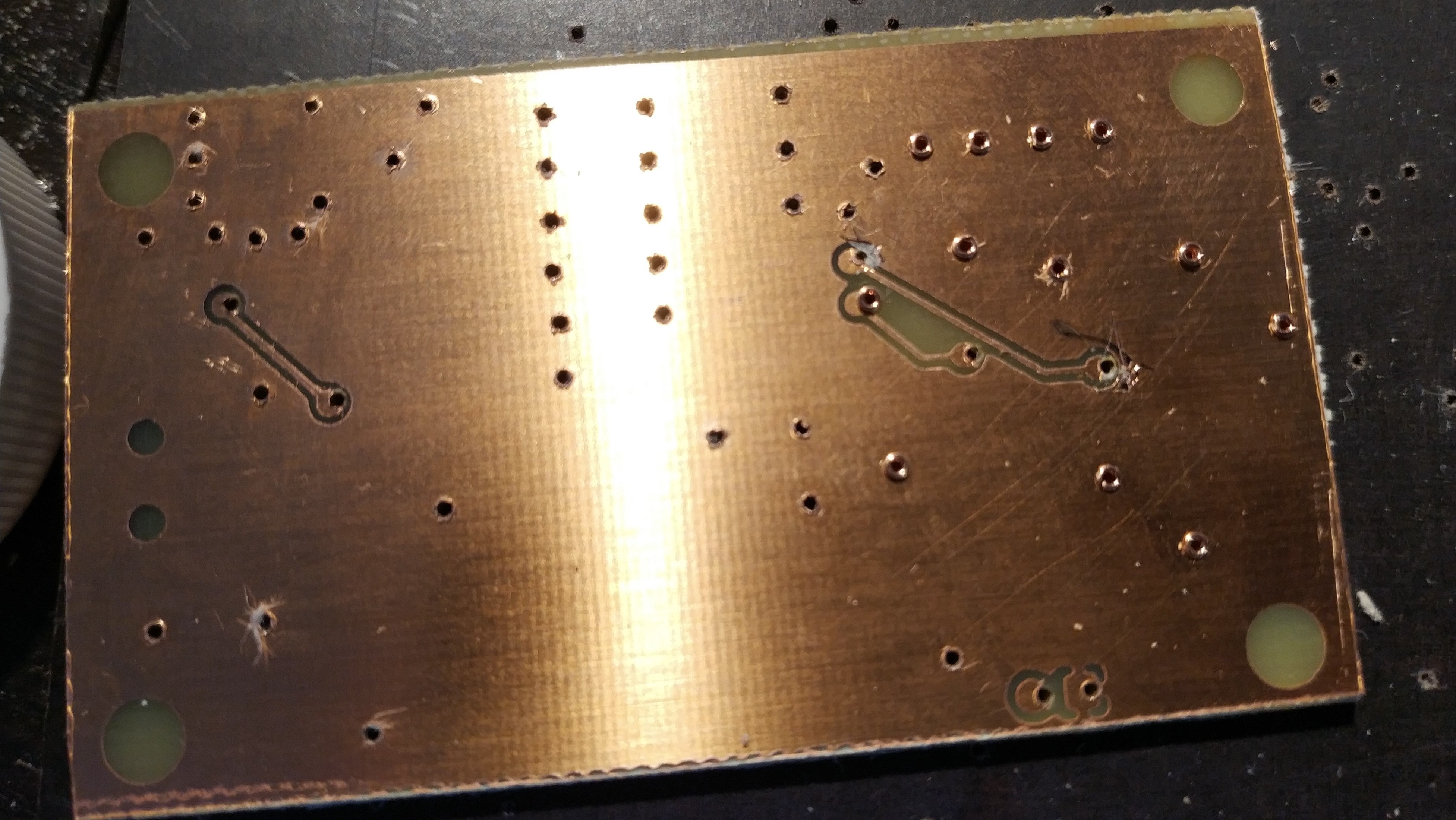
The second problem I will show here is exclusive for two layer boards: The front and back layer do not superimpose correctly. For a low density board like this one where only four vias were placed one can scrape the ground plane off and set the via anyway. For better connectivity of the via to the trace, you may tin both.![]()
![]()
-
Links
07/06/2020 at 17:06 • 3 commentsHere is a incomplete list of links of websites and programs you may find usefull when creating your PCBs.
Software to design the schematic and layout
- KiCAD (https://www.kicad.org/)
- LibrePCB (https://librepcb.org/)
- EasyEDA (Browser based, https://easyeda.com/)
Sources for parts and footprints which are not included in the software- SnapEDA (registration required, lots of parts for KiCAD, Altinum, Eagle, OrCAD, PCB123 and morehttps://www.snapeda.com/)
- KiCAD footprints and parts (https://www.kicad.org/libraries/download//)
- DigiKey library for KiCAD (https://www.digikey.com/en/resources/design-tools/kicad)
- Ultralibrarian (https://www.ultralibrarian.com/solutions/cad-vendors/kicad-pcb-libraries)
Changed the KiCAD urls to the new domain (kicad.org)
Yet another guide on how to make PCBs at home
Here I describe my method for making 1 and 2 layer PCBs at home via lithography and etching