Said Alvarado Marin
-
Safety and Risk Analysis Report
10/05/2020 at 13:11 • 0 commentsField Ready is an institution that take safety very seriously. They have entire articles explaining their very rigorous quality control and risk assessment protocols: https://www.fieldready.org/post/always-ready-with-quality-management
So, inspired by their Q&A video for this challenge. Were they explicitly said that having a complete Risk Analysis Report for both the builder of the project and the end user would be a mayor plus. We embarked in a mission to provide just that.We contacted a professional to help us prepare a full risk analysis report that is compliant with international guidelines for safety. The report covers both the user of the UV wand as well as the maker who has to build it.
You can find the full report right here:
UVA Project - Risk Analysis Report - English Version
UVA Project - Risk Analysis Report - Spanish Version
The rest of this log are some interesting calculations we did while validating the safety of the UV wand.
Measuring UV Irradiance
Irradiance is the amount of Luminous power that reaches a surface per unit of area. It is normally measured in miliWatts per squared centimeters. This measurement is important because its an indication of the intensity of light that is hitting a particular surface. The UVA Project was designed to irradiate.
As that is the amount of energy required to cure UV adhesives.
But, is this radiation dangerous? and are we actually managing to output so much power?
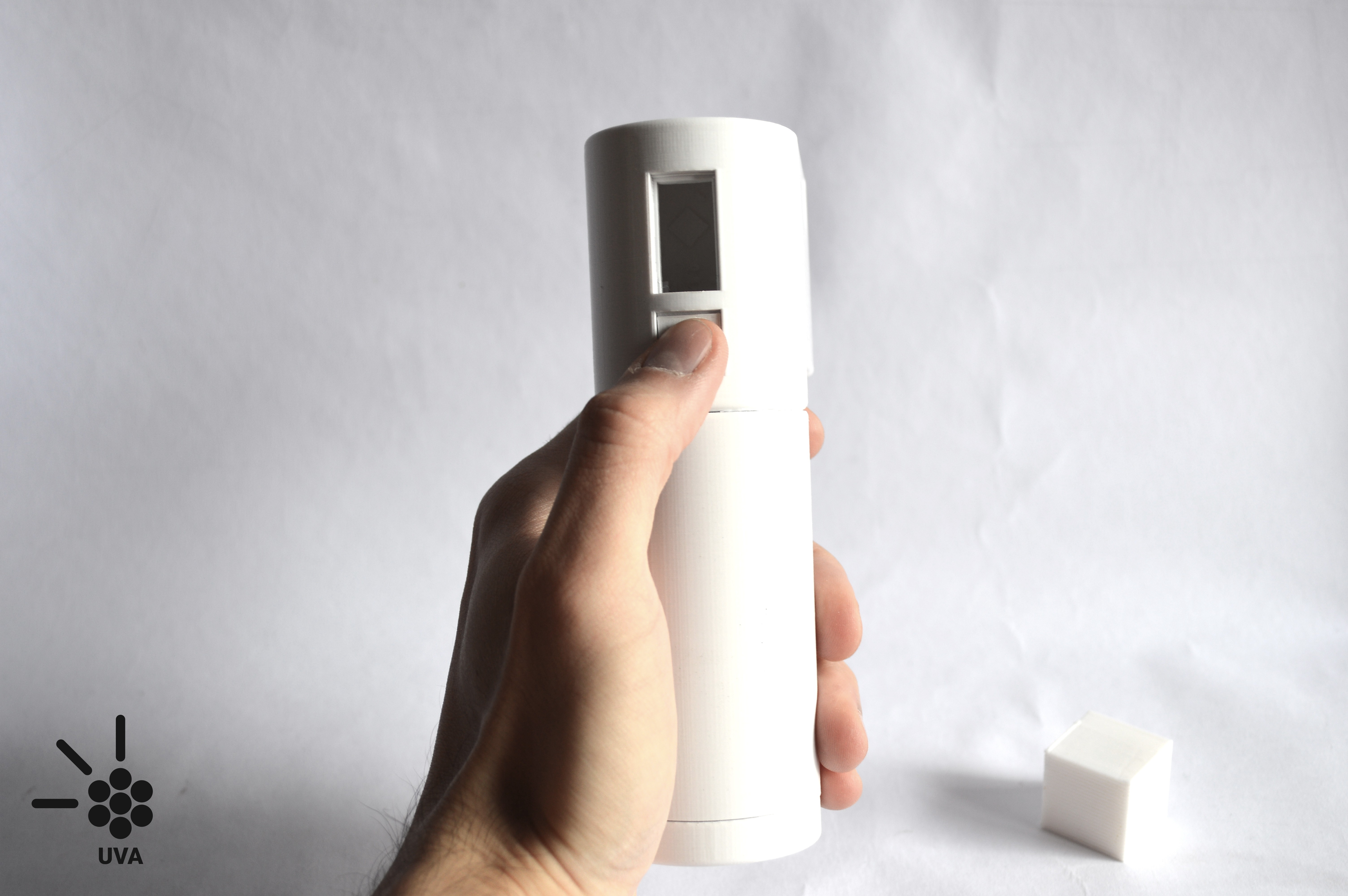
Let's start with the second question. To measure and validate the Irradiance claims of our UV wand, we bought a UV light sensor capable of calculating the irradiance of a source of light.
![]()
Image taken from Adafruit listing The VEML6070 is a small sensor capable of measuring the Irradiance of UV light at 365nm and report it with a precision of:
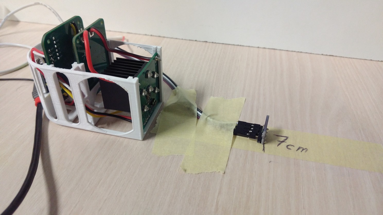
We prepared a small test bench to try the UVA project at different intensities and curent consumption. All measurements were made a 7cm from the LEDs, because that's theoretically the point of strongest Irradiance of this LED Bulb design (For more information, see here)
![]()
The results were as follows:
Relative Power [ % ] Current Consumption [ mA ] Irradiance [ mW/cm^2 ] 5 115 13.18 10 209 27.2 20 407 50.8 50 1050 104.2 70 1600 138 85 2050 147 100 2600 165 From this small experiment we learn that the UV Wand is quite more powerful than we anticipated. And that we only need to power it at 50% to achieve the desired Irradiance. This is excellent news because this results in less power being consumed, a longer lasting battery and less heat being generated
Having validated this value of 100mW/cm^2 we can now be sure that the calculations in the safety report apply to this UV Wand
-
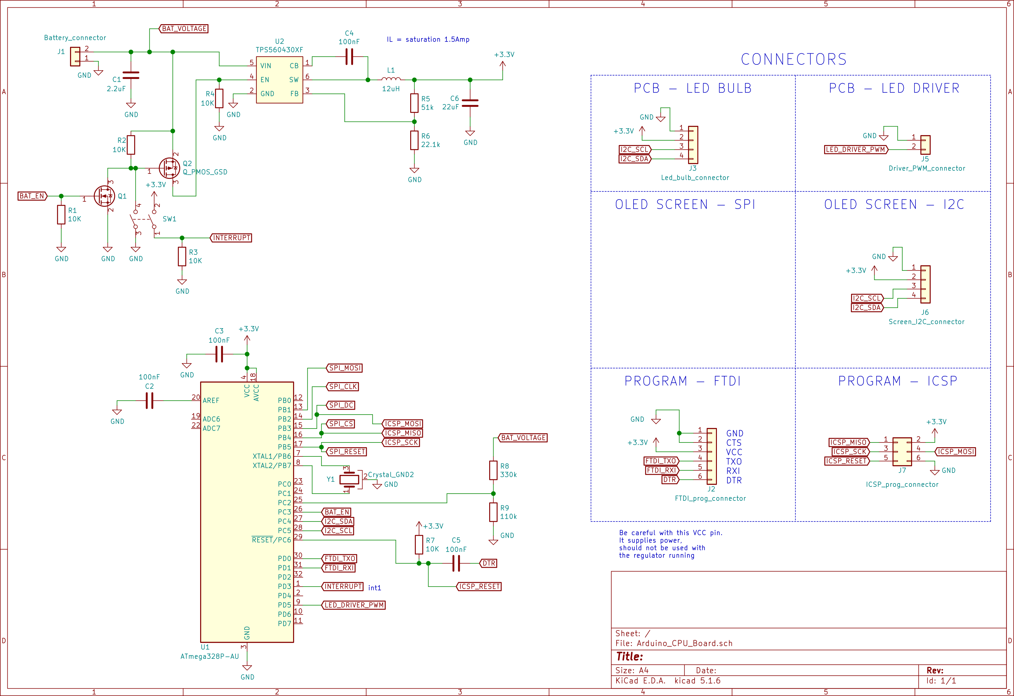
Custom Arduino Board Design
10/05/2020 at 11:57 • 0 commentsSince the UV flashlight has so many sensors, it requires a Microcontroller to read and manage everything. Of course, using the ever ubiquitous Arduino UNO chip ATmega328p is the obvious choice. As it greatly simplifies software compatibility later on. and this project doesn't really need anything more powerful.
![]()
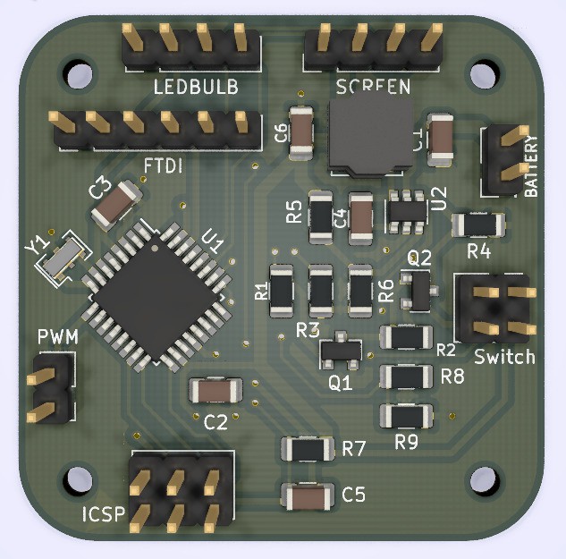
This board has a lot connections and parts, so let's do a breakdown and look at each of them.Power Regulator
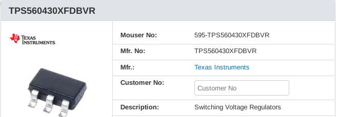
Image taken from Mouser's listing The Battery voltage is about 12V and the rest of the logic circuits run at 3.3v. We need a voltage regulator to step-down the voltage. The chosen part for this is the TPS560430XFDBVR. Here are some of the characteristics that made it attractive:- Inexpensive
- Low part count
- NON-QFN package (for easier soldering)
- The datasheet already pre-computes the entire circuit for a 3.3v ouput, so I didn't have to do any calculations. :D
Switch latch circuit
The main power on switch had a rather convoluted latch circuit to allow both the Arduino and the user to activate the main regulator's ENABLE pin. So that if a tactile button was used, the Arduino could remain ON even after the button was released.
It was taken from this website: https://circuitjournal.com/arduino-auto-power-off
It's still there in the circuit, but we found a switch that latches ON after being pressed, so the functionality wasn't needed.
Battery monitor
R8 and R9 form a voltage divider that allows the Arduino to measure the battery voltage. It's not a very precise method to estimate the remaining percentage of charge of the battery. But it is enough to provide a rough estimate of when the battery is too low. This way the Arduino can shut the LED's off and protect the battery from over discharging.
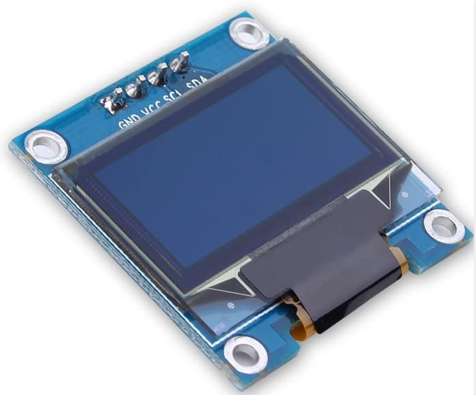
OLED Screen
Image taken from a listing in Amazon This is a little generic 128x64 0.96" Black & White OLED screen powered by a SSD1306 chip. They are widely available and have extensive software support.
Resonator
A crystal with a frequency of 12MHz was chosen for this board. Why the weird frequency? Because the ATMega328p can be unstable at 3.3v with a 16Mhz crystal. But 8Mhz is too slow for this application. So the fastest crystal we can use in this case is a 12Mhz one.
Programing connector
The board has 2 programming connectors. A ICSP connector to program the chip through SPI, and a Serial FTDI connector to program it through Serial.
However, for small incompatibility problems between the Arduino bootloader and an ATMEGA328p with a 12Mhz crystal (As is the case here). Right now, only the ICSP connector works.
Full schematics
Here is the full schematics of the board, if you can also find here the full Bll of Materials,
![]()
-
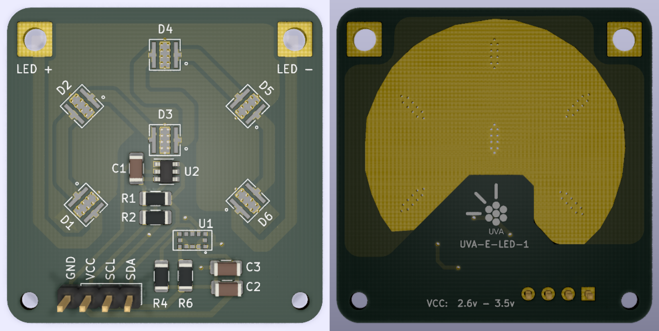
Designing a High Power Led Bulb
10/05/2020 at 11:04 • 0 commentsDesigning a 4x4cm PCB for LEDs that are supposed to handle up to 26Watts of power is not a trivial task. In this log we are going to take a look into the design process.
Most of the information and images from this log are taken directly from this amazing application note:
Optimizing PCB Thermal Performance for Cree® XLamp® LEDsIf you need to design PCBs for high power LEDs, this is where you should start. The application note is filled with thermal simulations and tests to figure out the cheapest and most efficient way of drawing heat away from your LEDs
Now then, the PCB we are going to be taking a look at is the following one:
![]()
It is supposed to hold 6 5Watts ultra violet LEDs, as well a couple of sensors on the front. And on the back have space for a big Heatsink.
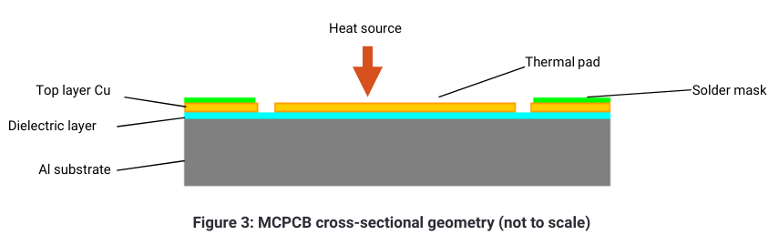
The goal
The main purpose of this PCB is to efficiently transmit heat away from the LED and into the Heatsink. This way we avoid over-heating and damaging the PCBs. The gold standard for this are MCPCB. Which (unlike most PCBs) are mostly made from aluminum to maximize their thermal conductivity.
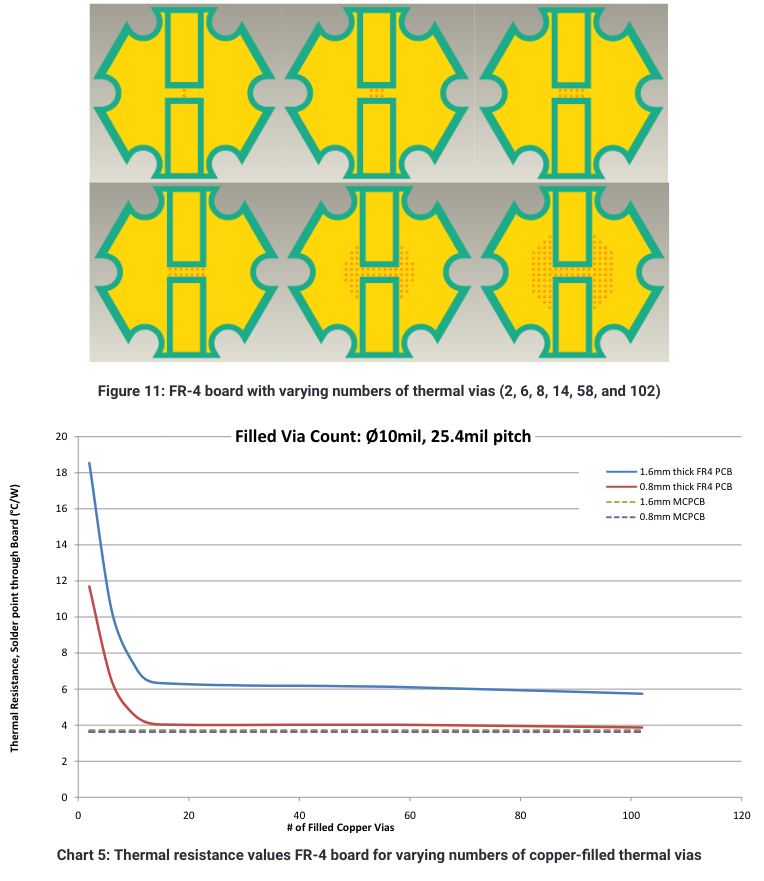
image taken from Cree's application note The problem with MCPCB is that they are rather expensive to manufacture. So it would be ideal to replicate this performance with the cheaper FR4 PCBs.Summary the Cree's Application Note
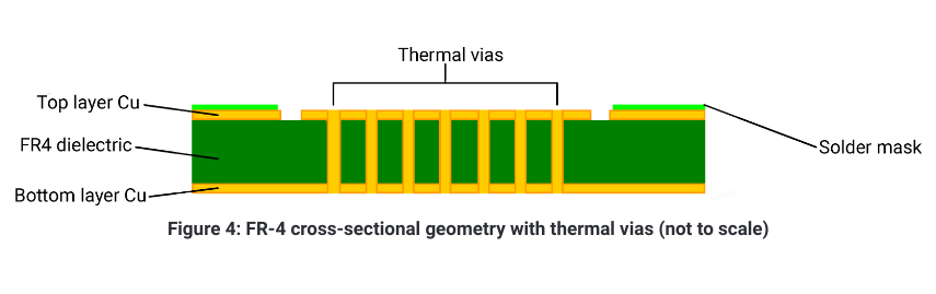
The Application note proposes that it is possible to dramatically increase the thermal conductivity of a FR4 PCB by making it very thin and adding a ton of thermal vias, like in the following diagram:
Image taken from Cree's application note The document has a bunch of really cool simulations where they test several different factors of the PCB. Like for example the following where they validate that thermal vias are useful, but only really worth it if they are directly below the LED.
Image taken from Cree's application note Of all the factors discussed and taken into consideration. I used took away the following 4 for my design
Most important considerations
- The thinner the PCB the better. 0.8mm thick gives good results
- The thermal vias should be as small as possible. They use and recommend 0.25mm diameter
- Place as many vias below the LED's thermal pad as you can.
- Maximize the copper area in contact with the Thermal vias both at the front and at the back of the board.
- If it's possible to fill the thermal vias with solder while you're assembling the PCB, good. That also helps.
Implementing the recommendations
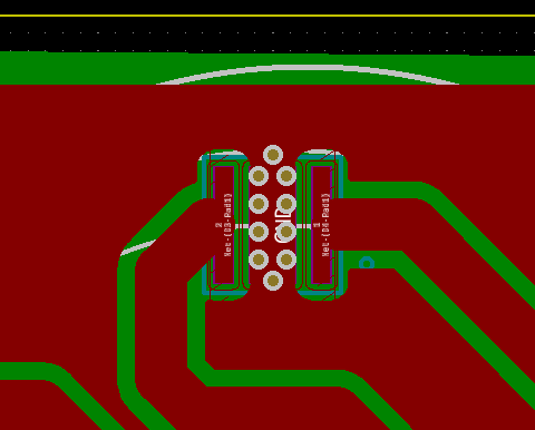
Single footprint of an LED in Kicad Let's concentrate on the footprint of a single LED.
- The vias had to be 0.3mm in diameter because that's the smallest the PCB manufacturer would allow
- A total of 10 vias fitted right below the Led
- Both front and back the thermal pad is connected to large copper planes
- The PCB was manufactured at 0.8mm tick instead of the more standard 1.6mm
It is laborious work to set everything up like that. But the results were good with this configuration.
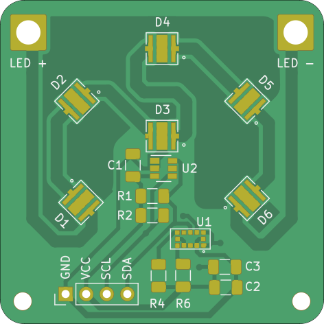
A word on the schematics
![]()
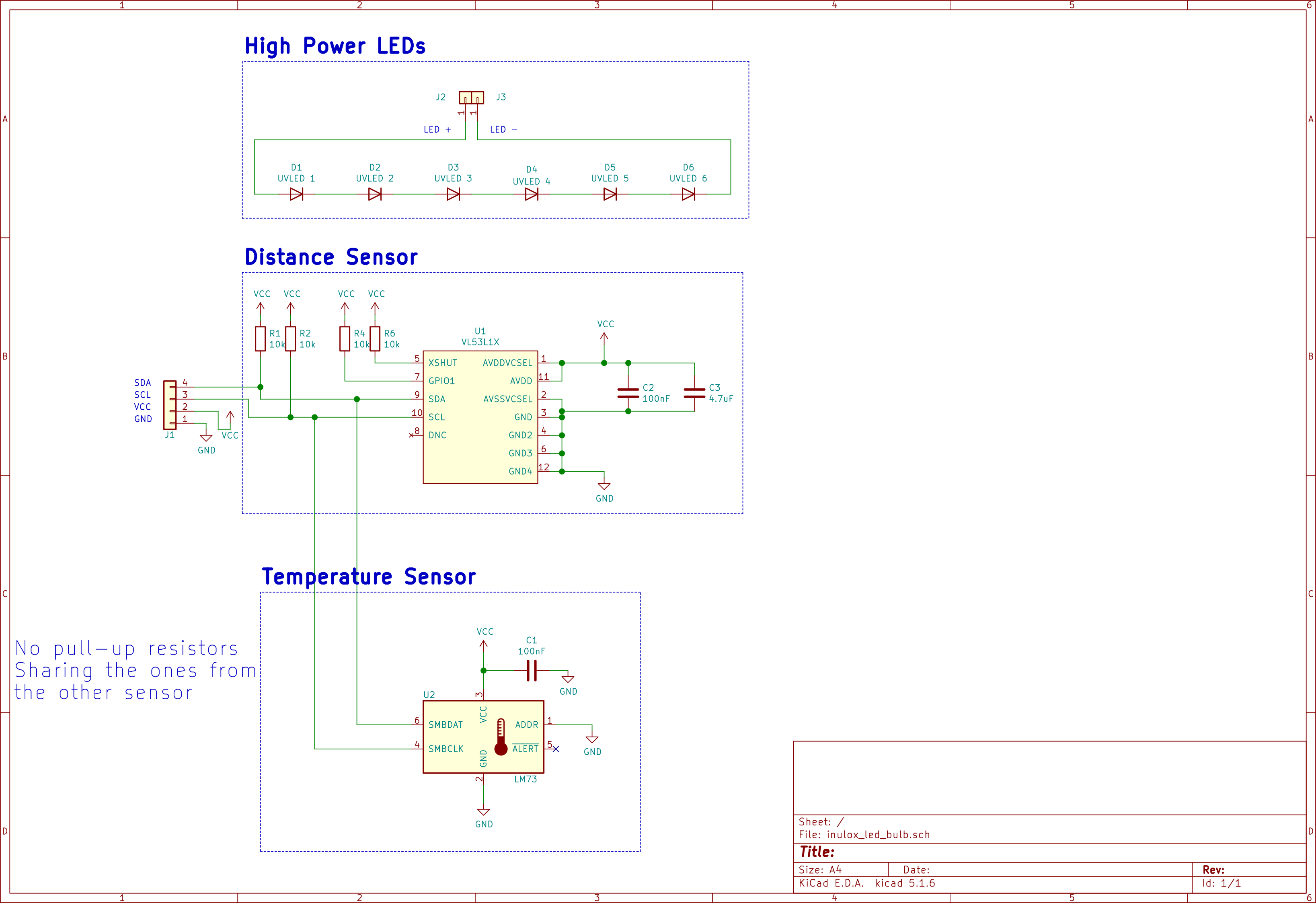
This PCB also houses a couple of sensors, namely U1 and U2:
Temperature Sensor - LM73
Image taken from Mouser's Listing This is a small I2C digital temperature sensor from Texas Instruments. It helps monitor the temperature of the LEDs to make sure they are not overheating. It was chosen mostly because it was the only small I2C temperature sensor, with good library support and in a NON-QFN package (to simplify soldering.) that I could find.
It was installed as closed to the LEDs as possible. And It's ground pin was connected to the LED's Thermal plane, to improve thermal transference between the LED and the sensor.
Distance Sensor - VL53L1CX
Image taken from Mouser's listing We would also like to monitor the distance from the LED to the closest surface. So we chose a small distance sensor to accomplish this task. Since the Flashlight has to operate in an environment of high luminous intensity, be it outdoors or on it's own High power UV reflections, all reflective-based sensor were disqualified. Which is why we chose with this Time-of-flight sensor. Which is conveniently controlled through I2C. Sadly it comes in a QFN package, but there is not much we can do about that.
It was installed far away from all the heat generating components.
Full schematics
The schematics of both sensors are very straight forward. They only need a handful of capacitors and resistors, which the datasheet points of how to select. The final schematics for the PCB is the following:
![]()
-
LED driver - PCB Design
10/05/2020 at 09:22 • 0 commentsIn this short log were are going to talk about some of the consideration taken into consideration when designing the PCB for the High efficiency Led Driver.

High Efficiency LED driver PCB AL8853 datasheet recommendations
Thankfully, as with many integrated circuit nowadays, the AL8853 Led driver datasheet has a handful of recommendations layout. In this case they are pretty basic:
- Keep traces thick and short.
- Keep capacitors and resistors as close as possible to the IC.
- Keep delicate signals away from inductors.
- Make sure these high current loops are as short as possible.
The loops they are talking about are these ones:
image taken from the AL8853 datasheet Which in our PCB, correspond to the following traces:

Which realistically speaking, are about as small as I could feasible make them.
A word about EMI transmission
I do not know much about PCB design in general. But in this excellent resource over here, they recommend the practice of via stitching to minimize the amount of electromagnetic interference your board will generate.
So if you check the Kicad project for this board and wonder why there are so many random vias everywhere. This is the reason. -
Fabrication costs
10/04/2020 at 22:15 • 0 commentsAs field ready states in the design brief, Standard benchtop UV cure stations cost more than a 1,000 USD. Also are highly energy demanding and are not so flexible. We are so glad to say that we managed to address all the requirements proposed by Fielded. We design a UV wand, open source, with enough power to cure UV adhesives, flexible (considering that is a multitool kit with the possibility of design different tools for the battery pack), energy efficient. And of course, cost effective.
The total amount that we spend in materials, components and shipping to create one unit of UVA-1 was:
203.16 $ USD
Now the specific costs of every part of the project:
- PCBs fabrication 15$ (5$ each)
- UVA-E-LED-1
- UVA-E-CPU-1
- UVA-E-DRV-1
- PCBs Shipping 22$ (In total)
- PCBs Paypal fee 2$
- UVA-E-LED-1 Components 91.61$
- UVA-E-CPU-1 Components 7.14$
- UVA-E-DRV-1 Components 6.59$
- AZ-Delivery Oled Screen 7.36$
- 18650 Battery (3 cells) 34.23$
- Switch TL2230 1.12$
- ATS Heatsink 9.13$
- Battery Contacts (8) 1.44$
- Wire TUOFENG (1M) 1.40$
- Filament eSun (147gr) 3.78$
- Electricity 2.7Kw/h (3D Printer) 0.36$
- PCBs fabrication 15$ (5$ each)
-
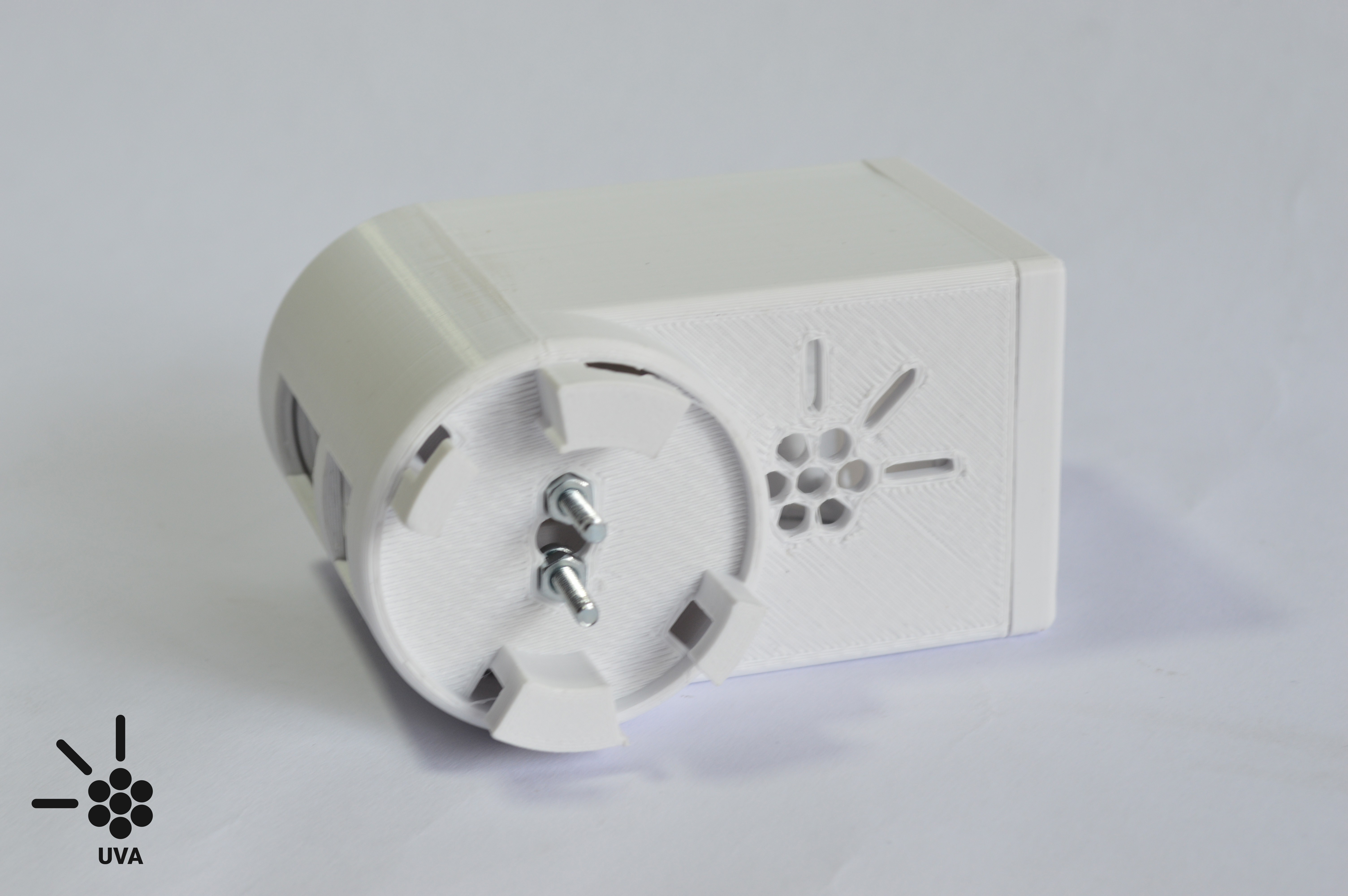
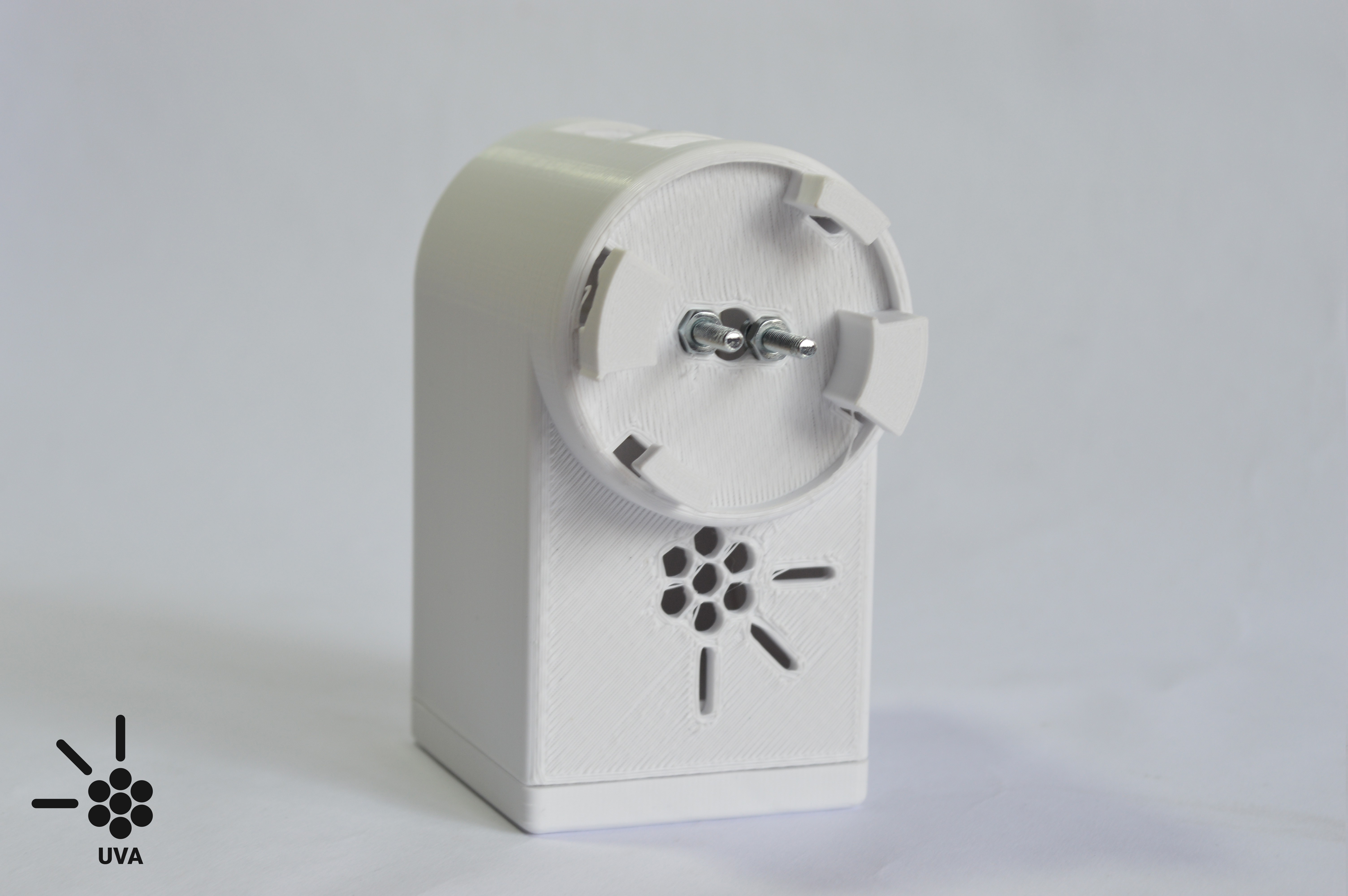
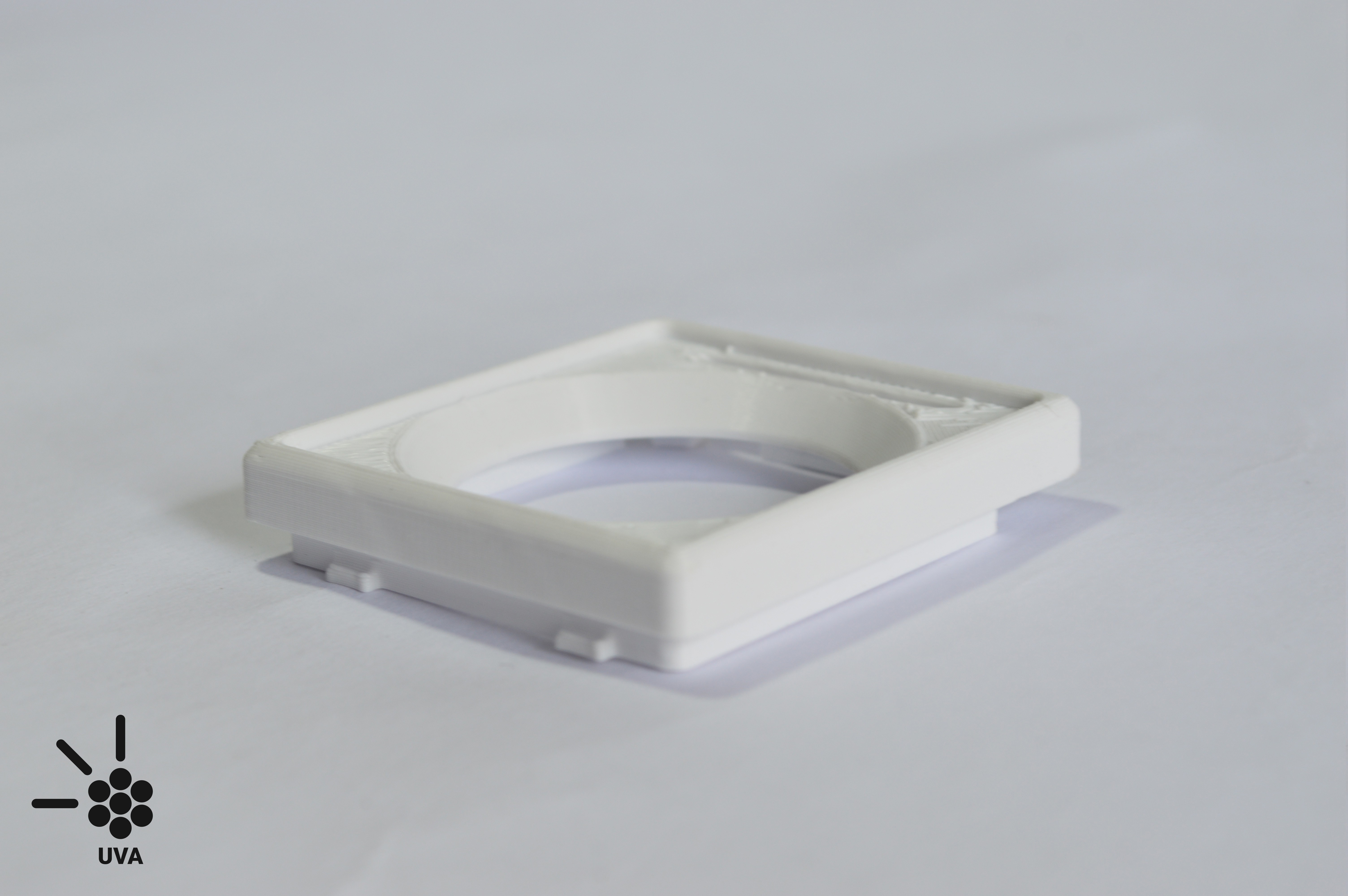
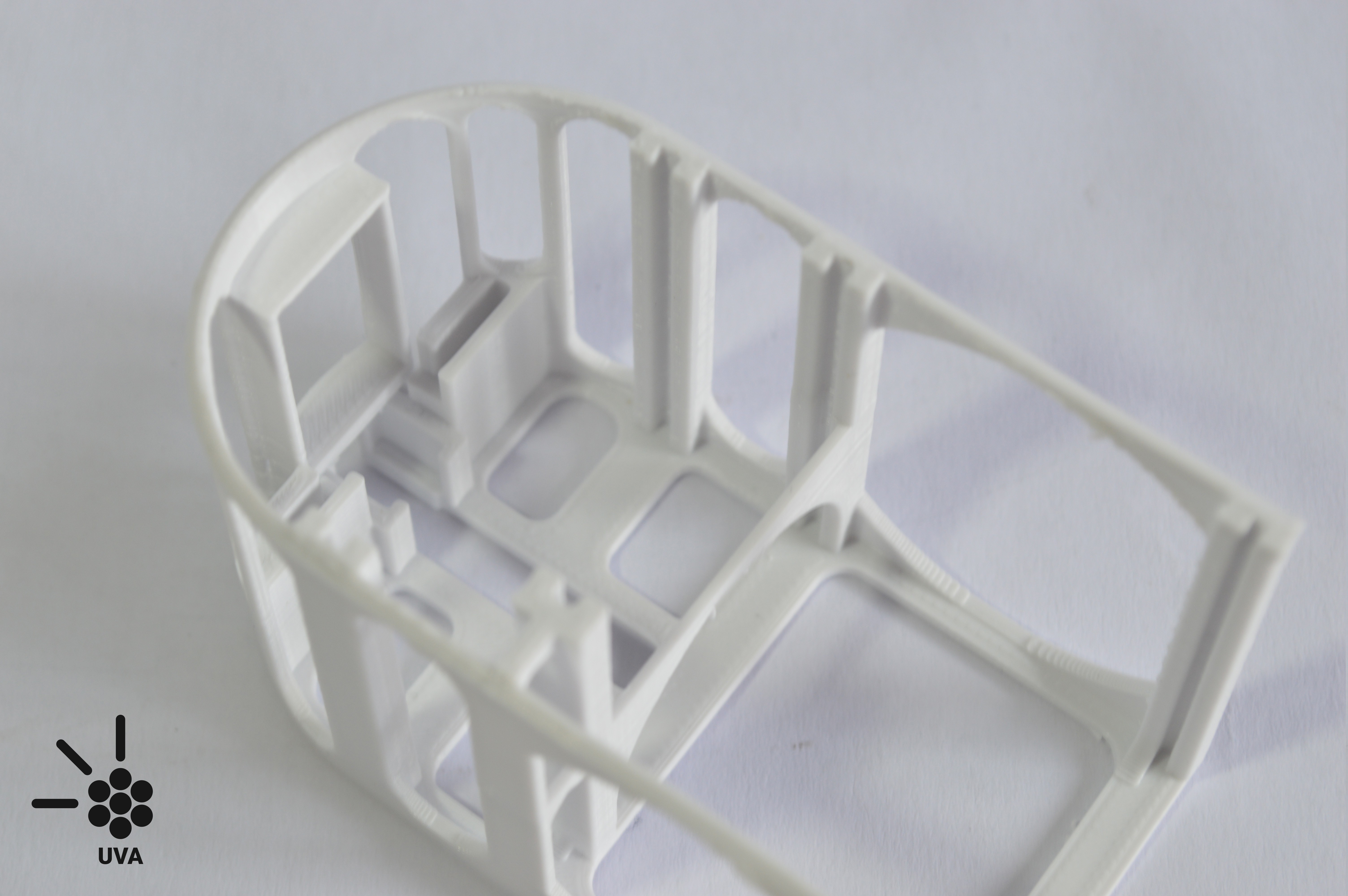
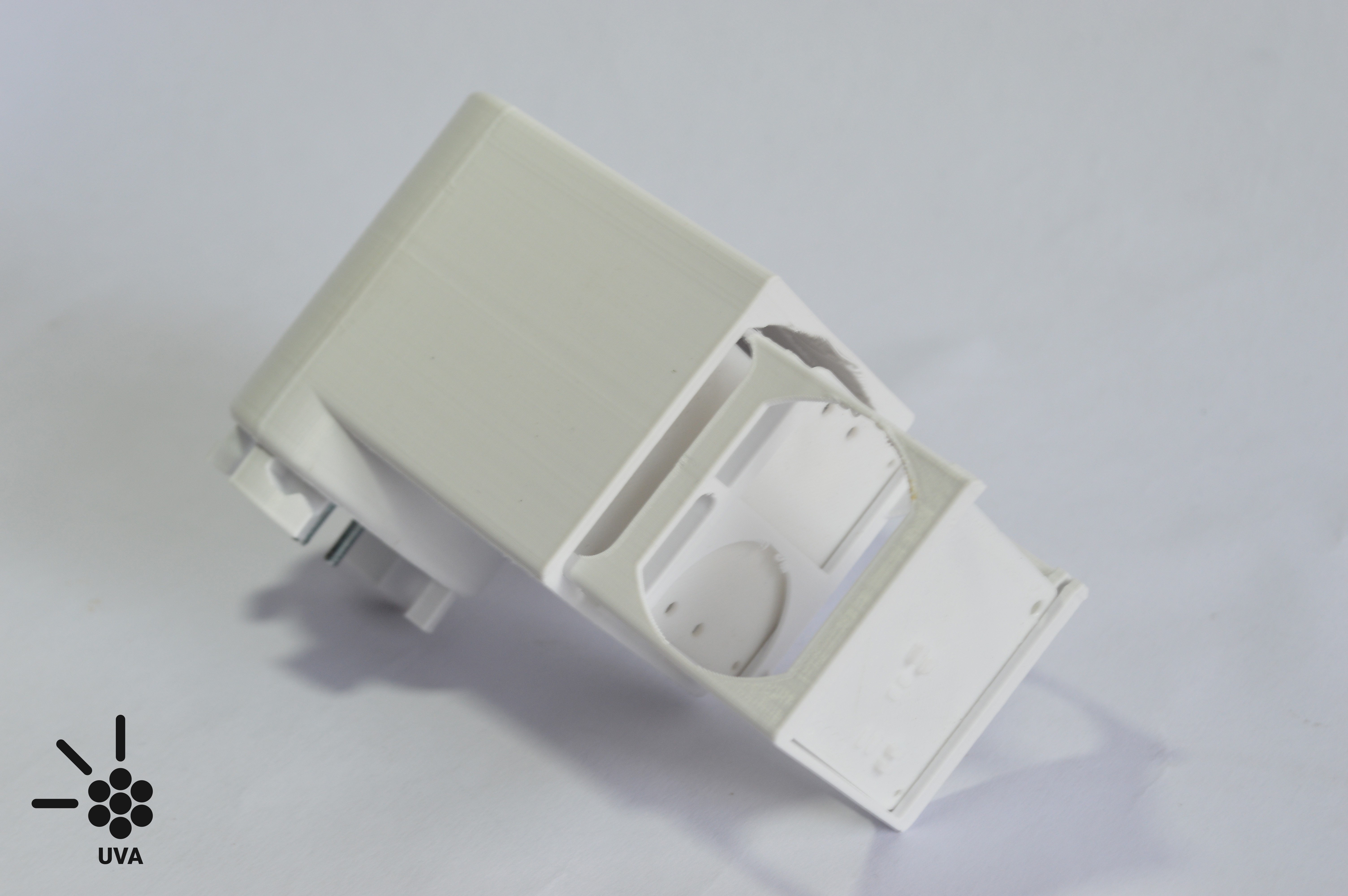
UVA Head
10/02/2020 at 14:59 • 0 comments![]()
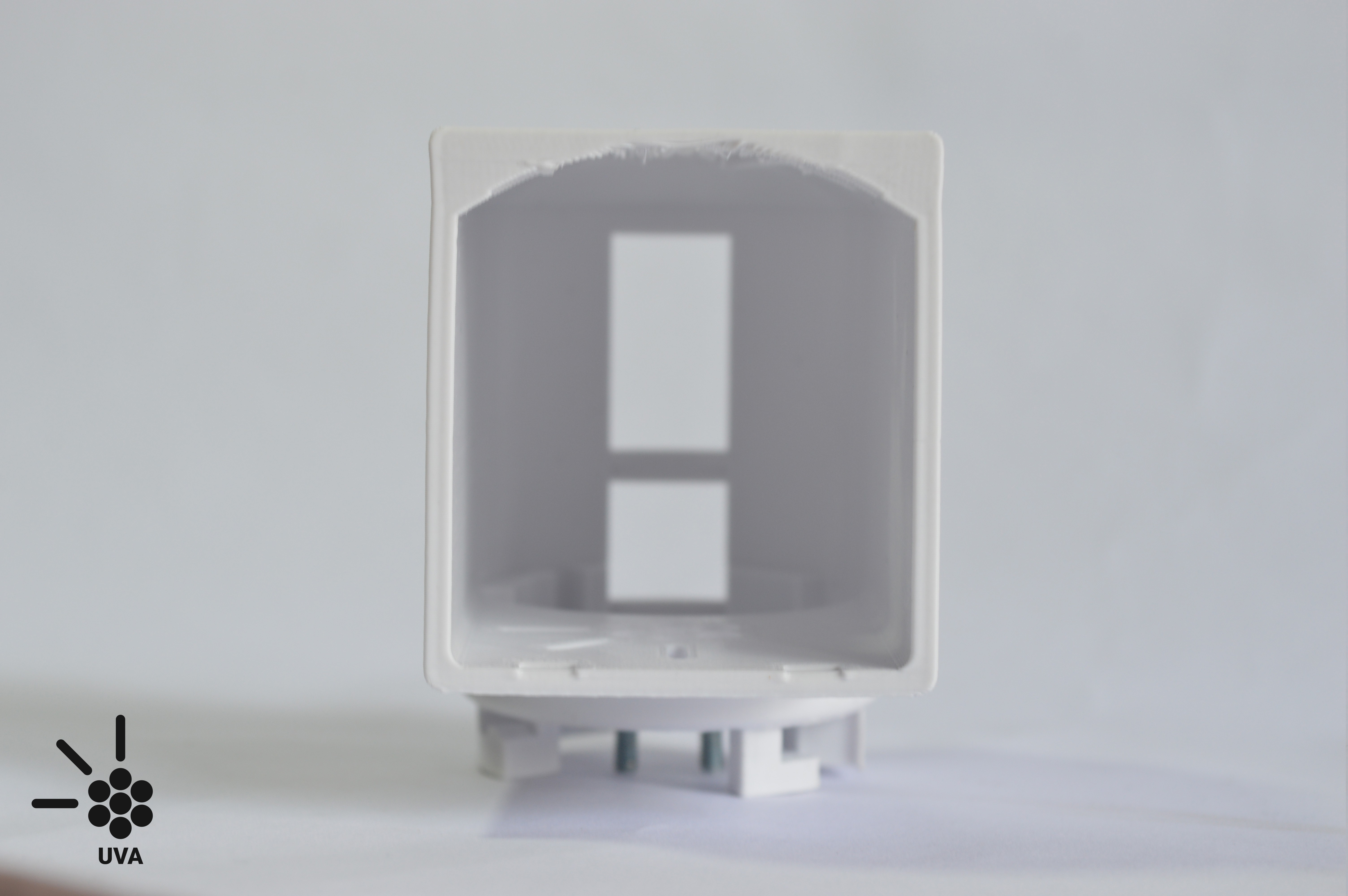
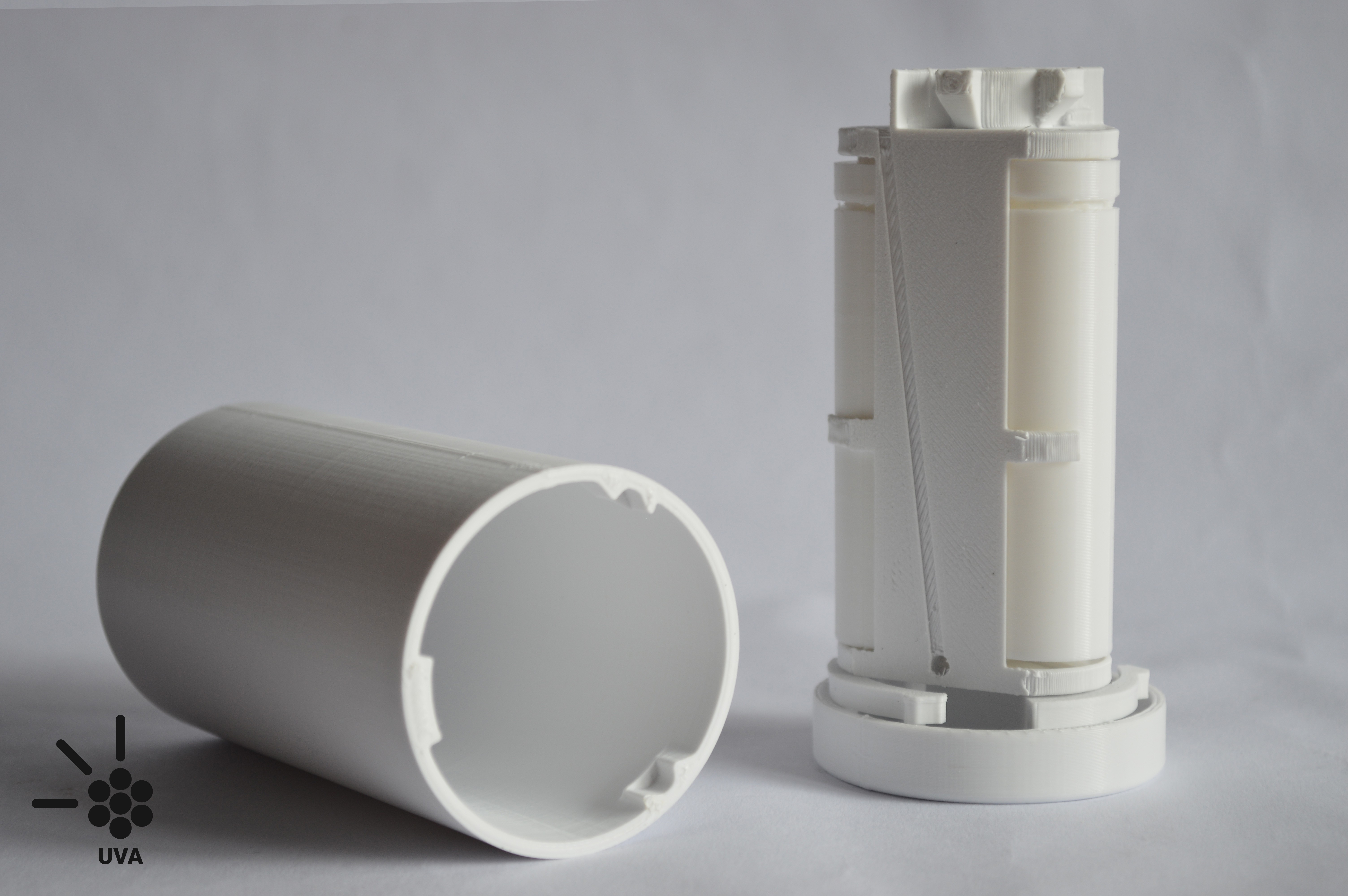
This part of the tool is the main event, even so, we design a multi-tool kit, we put all our effort to create the best solution to address the challenge that Field Ready put in our hands. In this case, this log will be only about the design aspects of the head, the electronics will be addressed in specific logs.
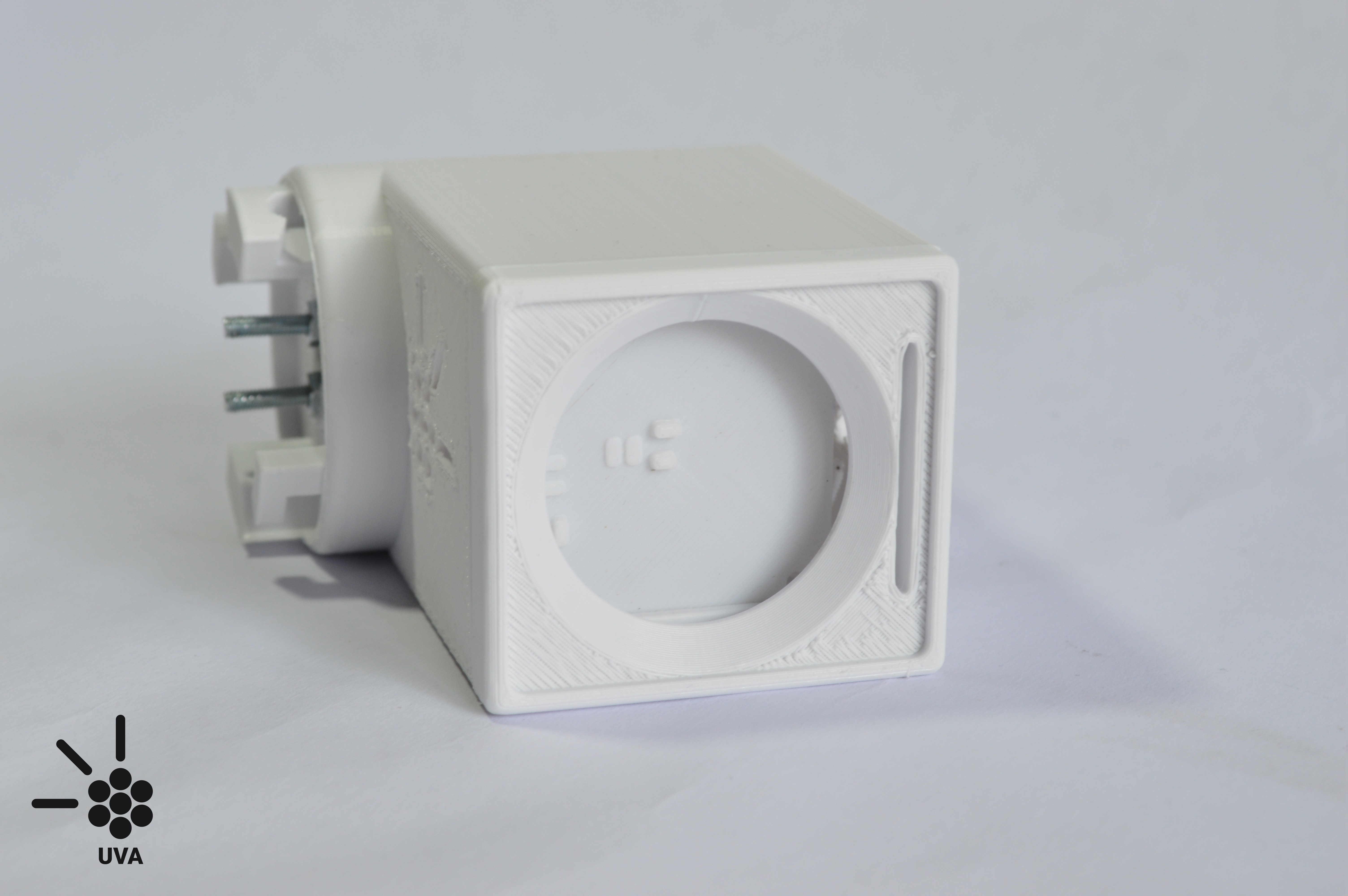
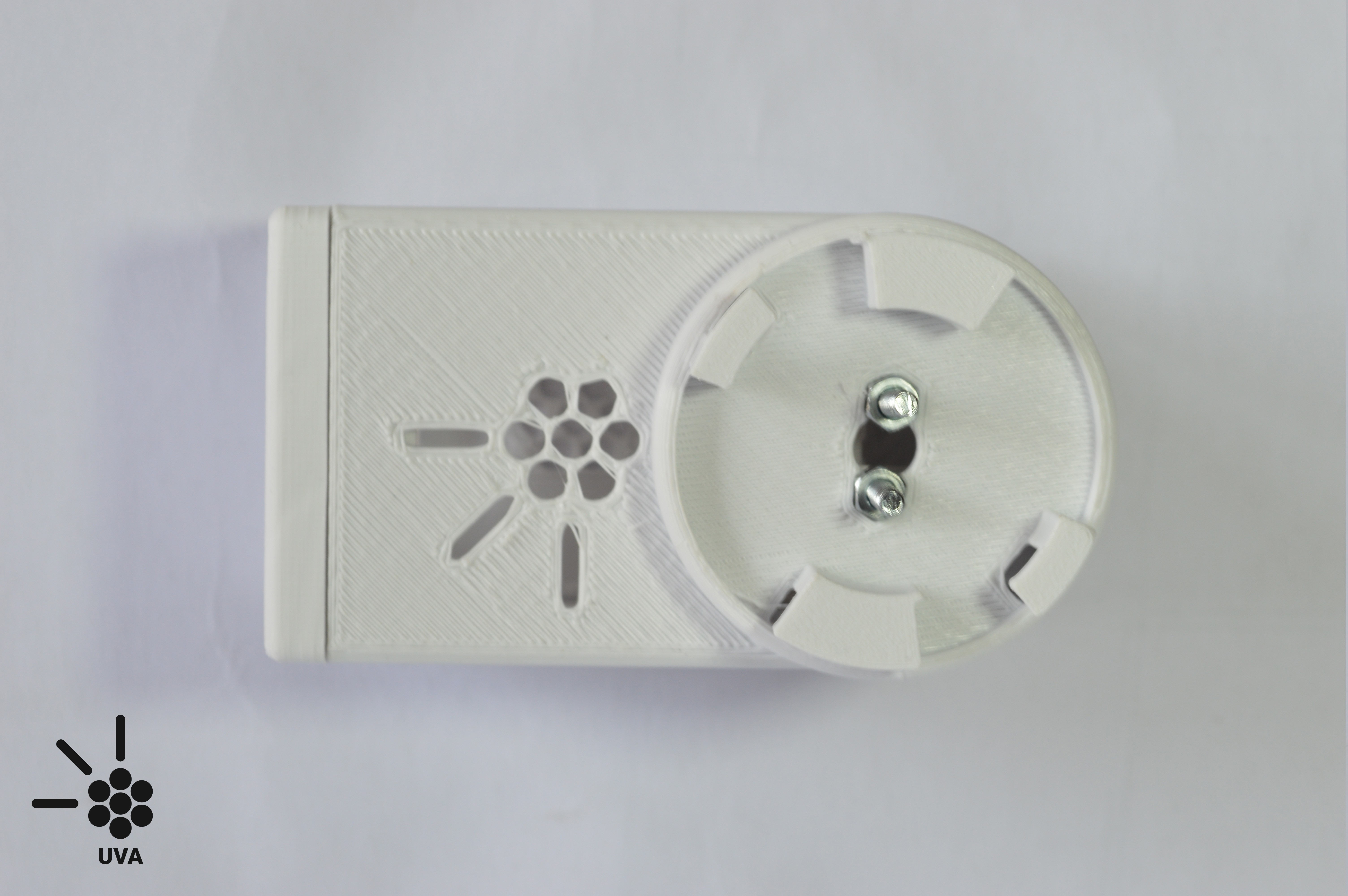
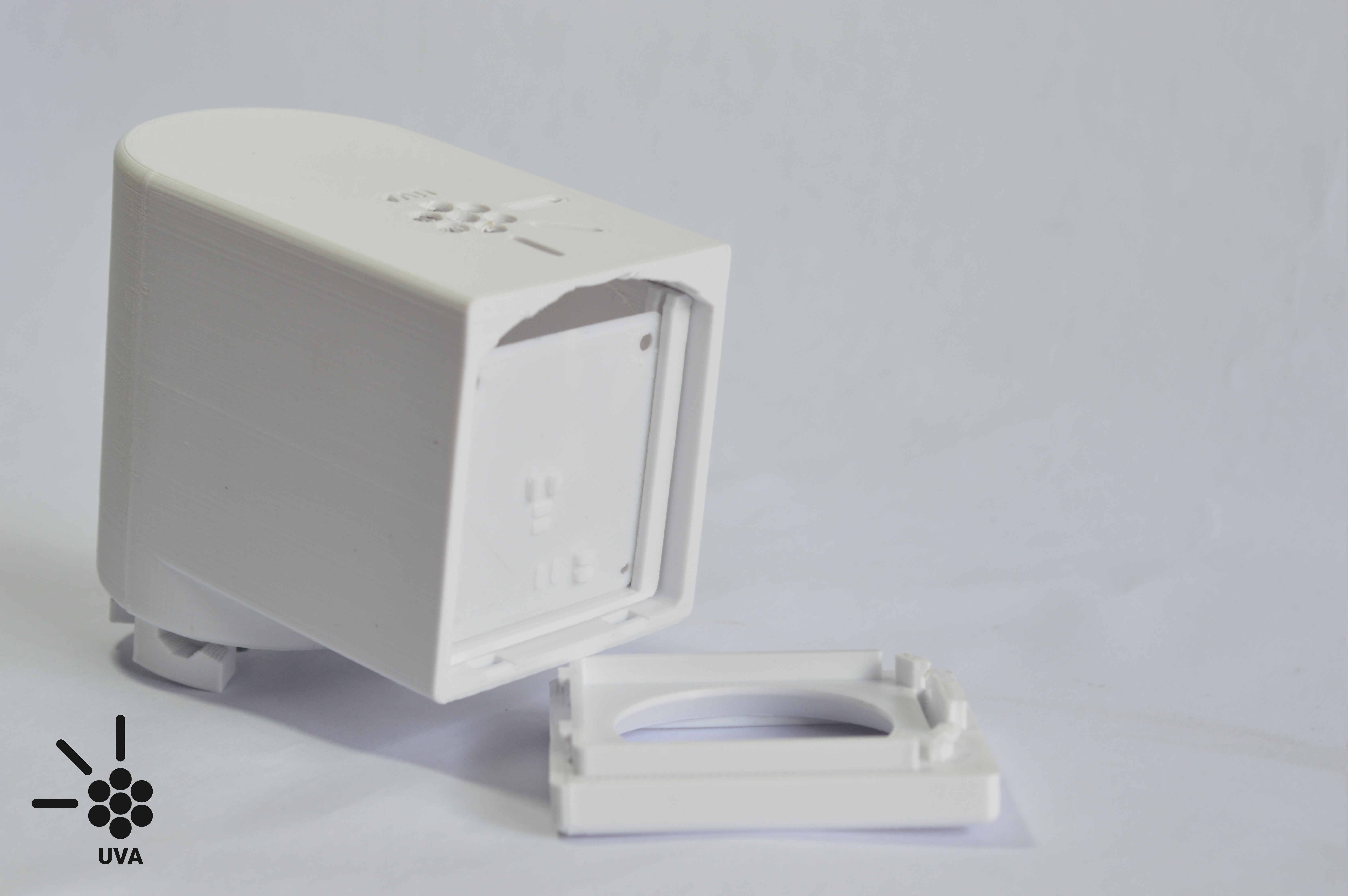
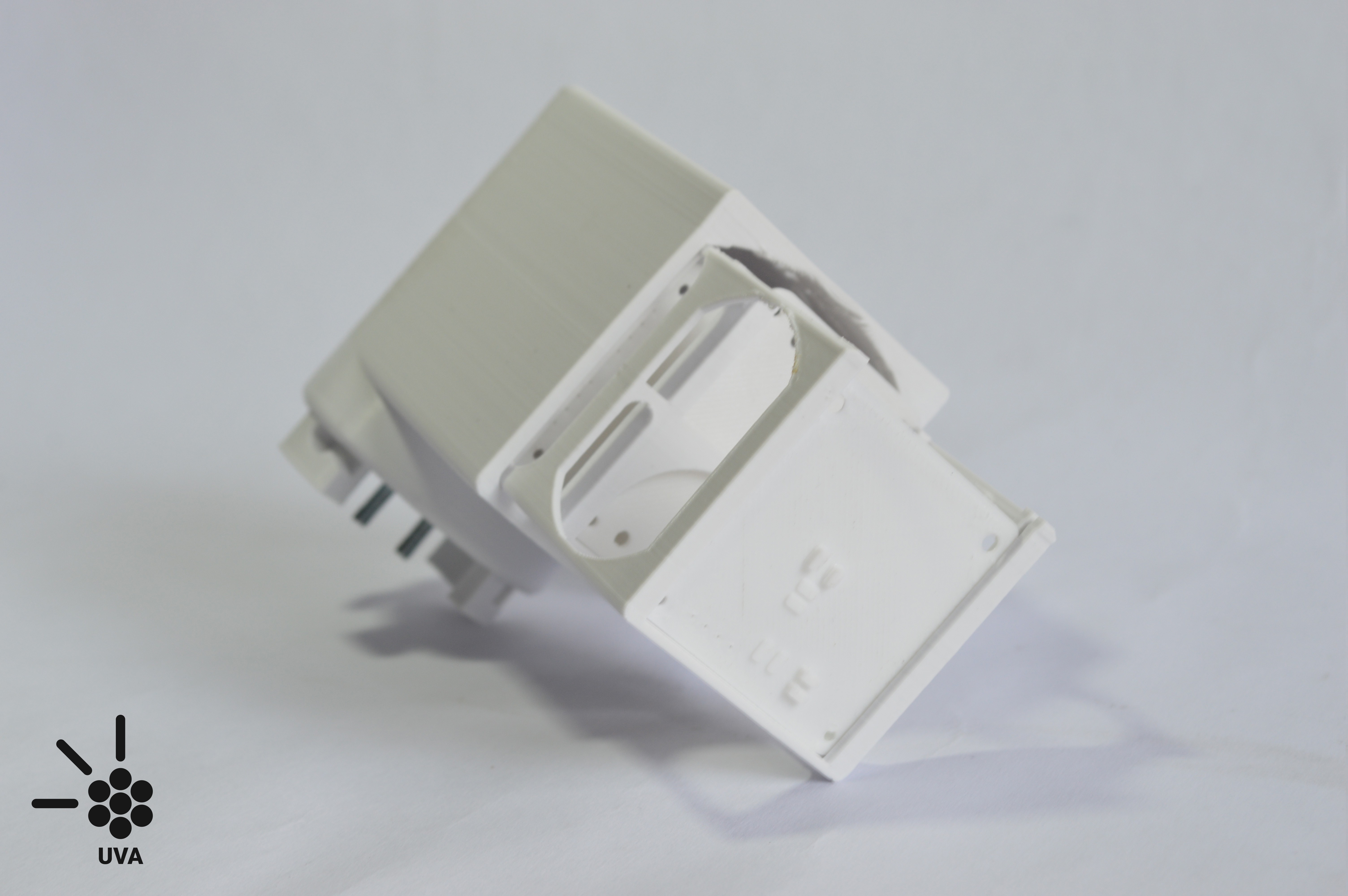
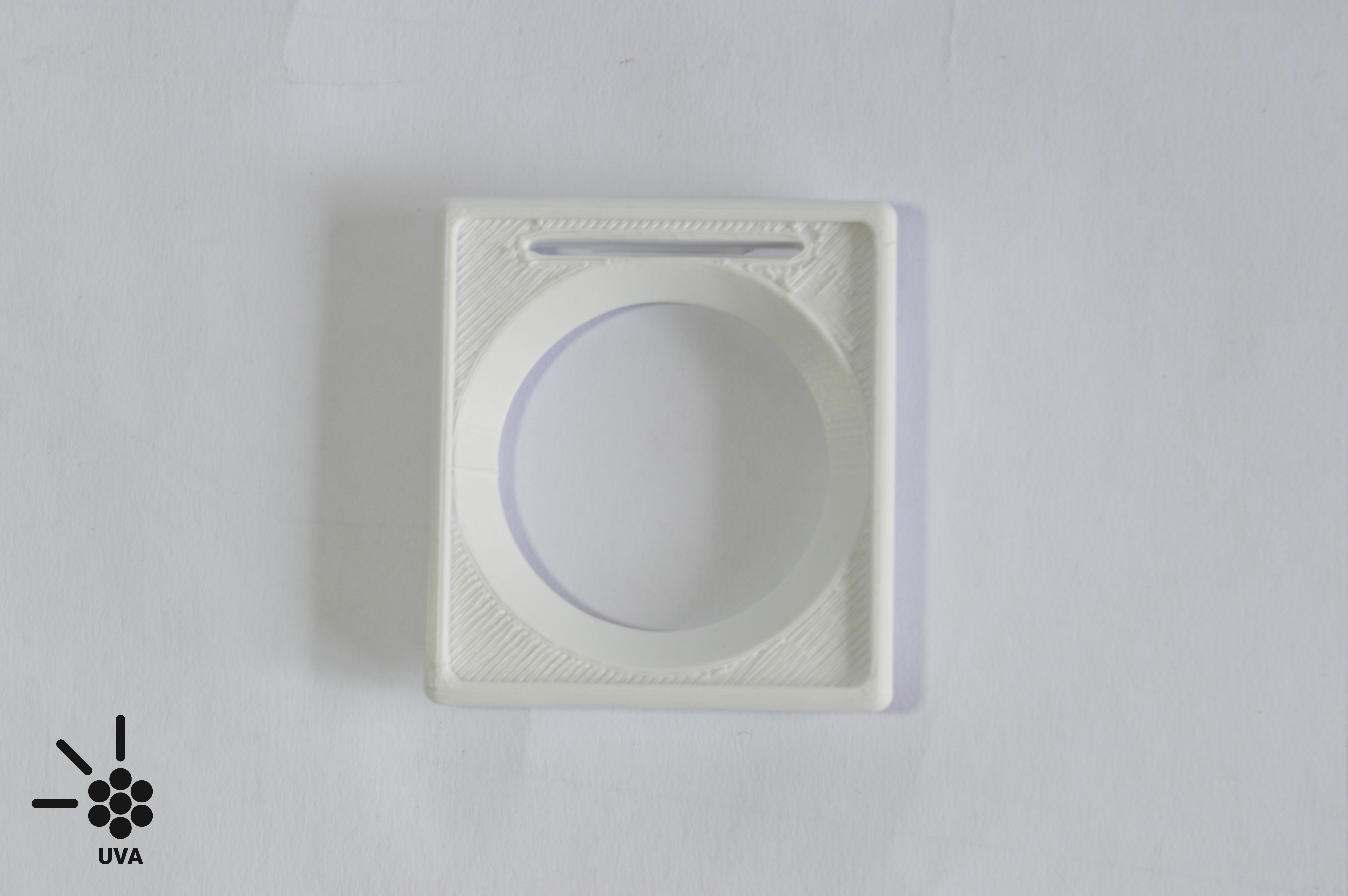
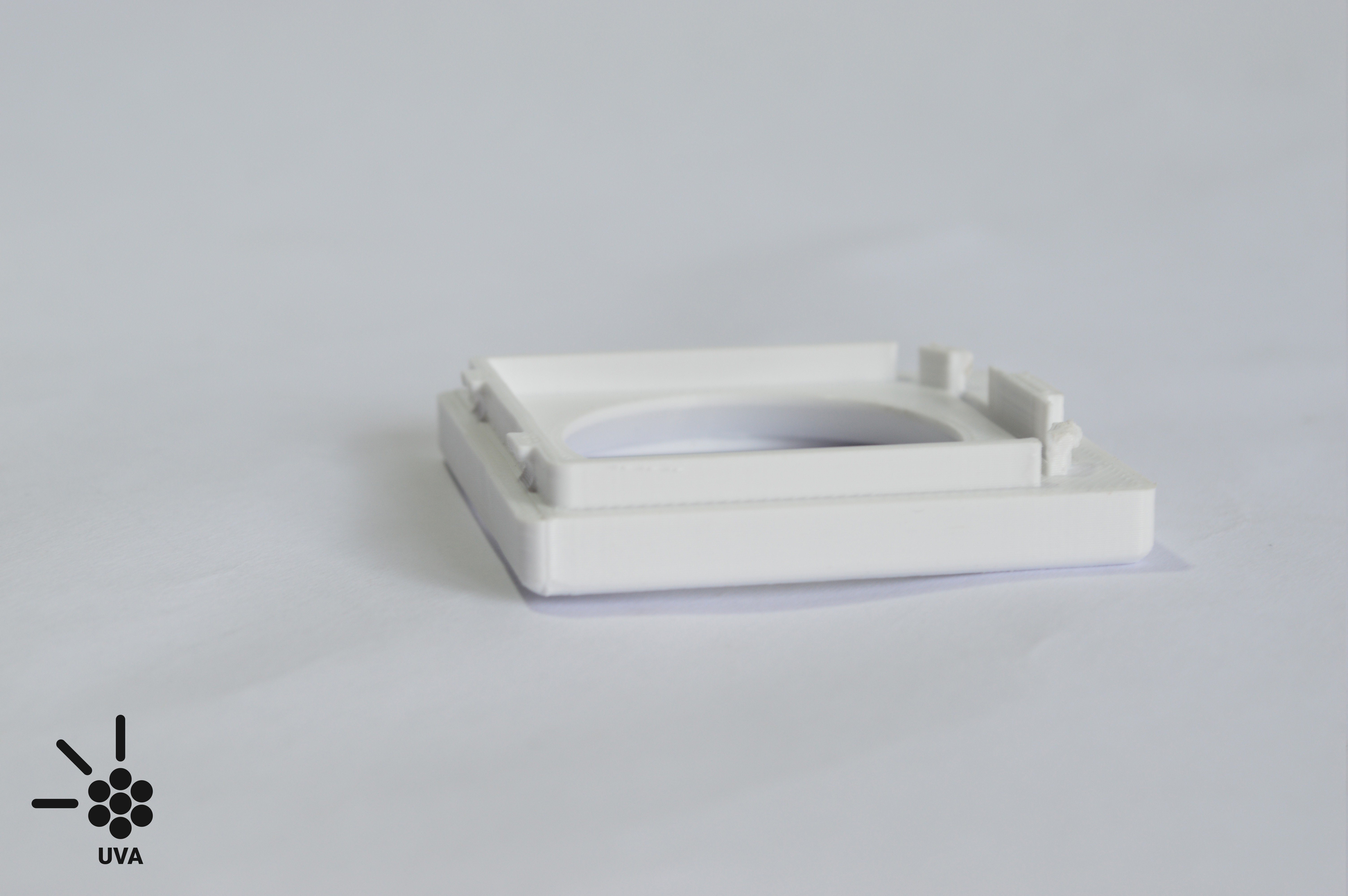
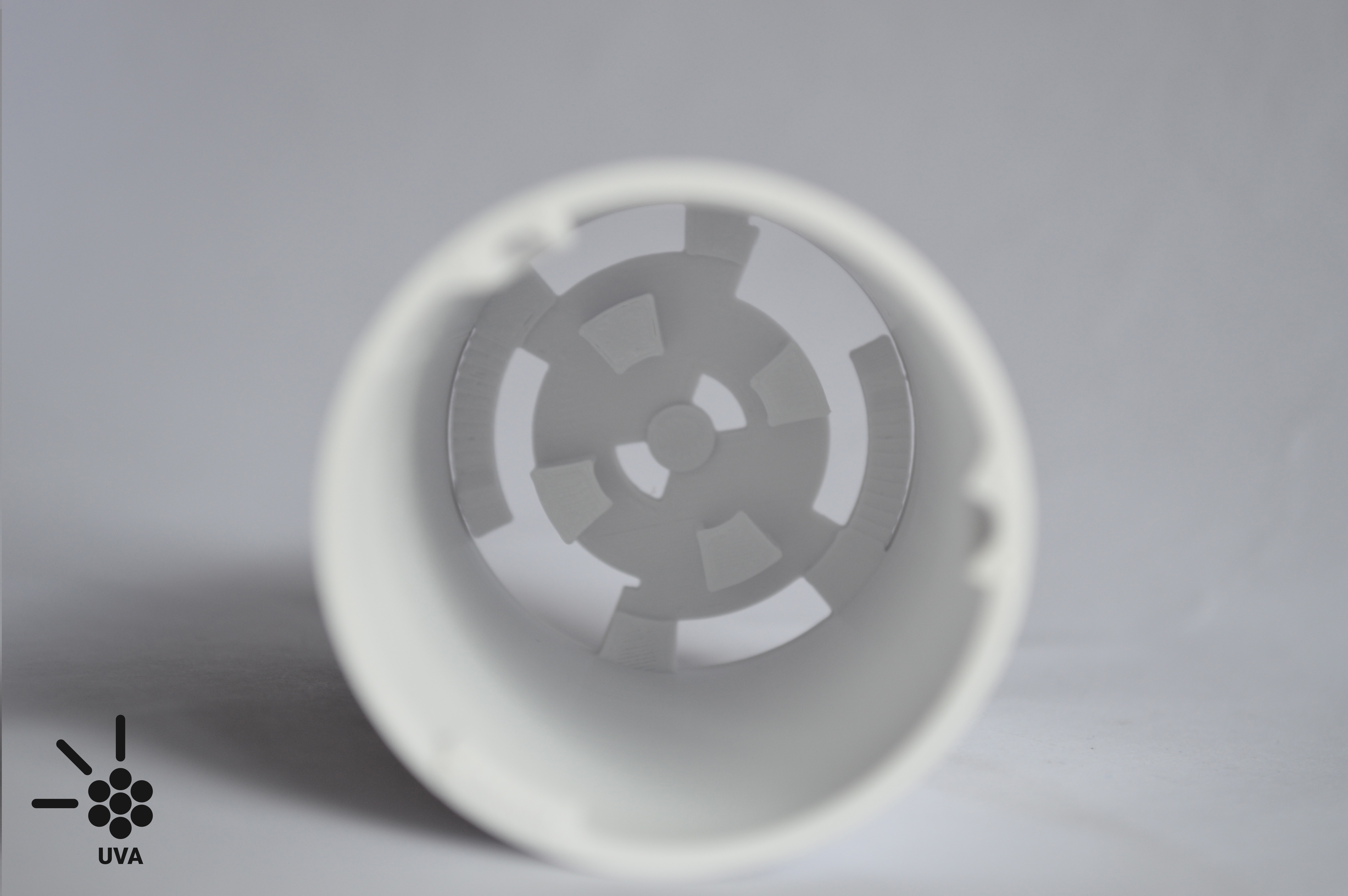
About the design. Like the battery, the UVA head is a modular design that consists of four 3D printed parts (The Chassis, the button, the front closure, and the circuits rack). Every circuit and component have it place in the rack (the UVA led board, the power source board, the screen, the button, and the CPU board). Also, the Chassis has the space to put Two 3M screws of 15mm long with them nuts to transmit the electricity from the battery to the circuits and are part of the UVA joint.
![]()
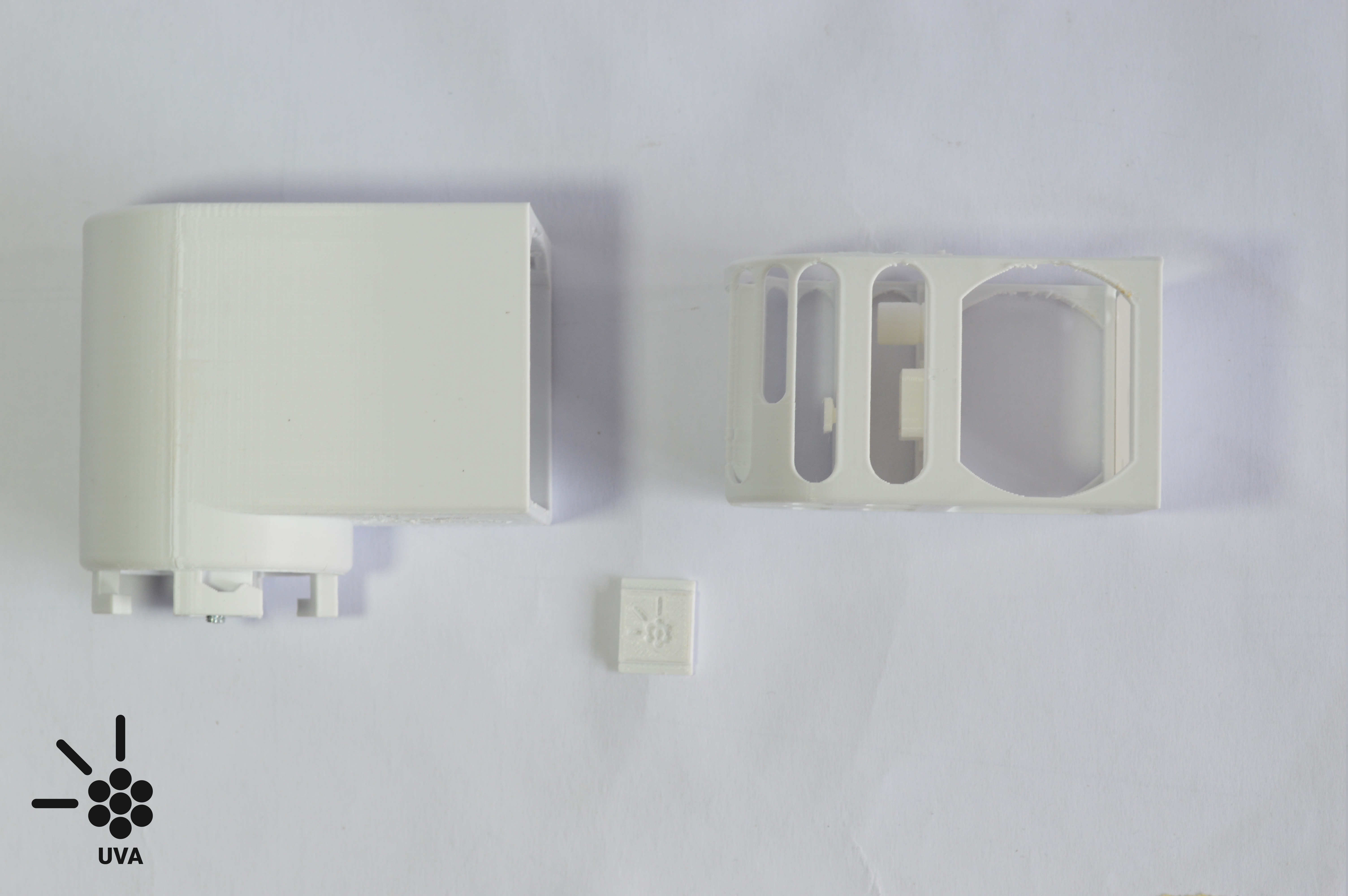
The chassis was designed to be printed without any support insight to facilitate the production and ensemble of the UVA. It was quite difficult and the insight finish of it is not the best but it is a great solution with a segmental arch taken from colonial Spanish architecture. It allows to reduce the height of the arch and keep a reduced size for the UVA head.![]()
Even so, there are some supports outside that you have to manage to remove, but it was not so difficult. Even so, in further prototypes, we would like to reduce more the use of supports.
Al, the rack slices insight into the chassis, and all the connections were designed without glue, only by rotations and pressure. Also, we want to have a one-piece chassis to increase the resistance of it to avoid damages to the electronics and circuits.![]()
![]()
![]()
![]()
![]()
![]()
![]()
![]()
![]()
![]()
![]()
![]()
![]()
![]()
-
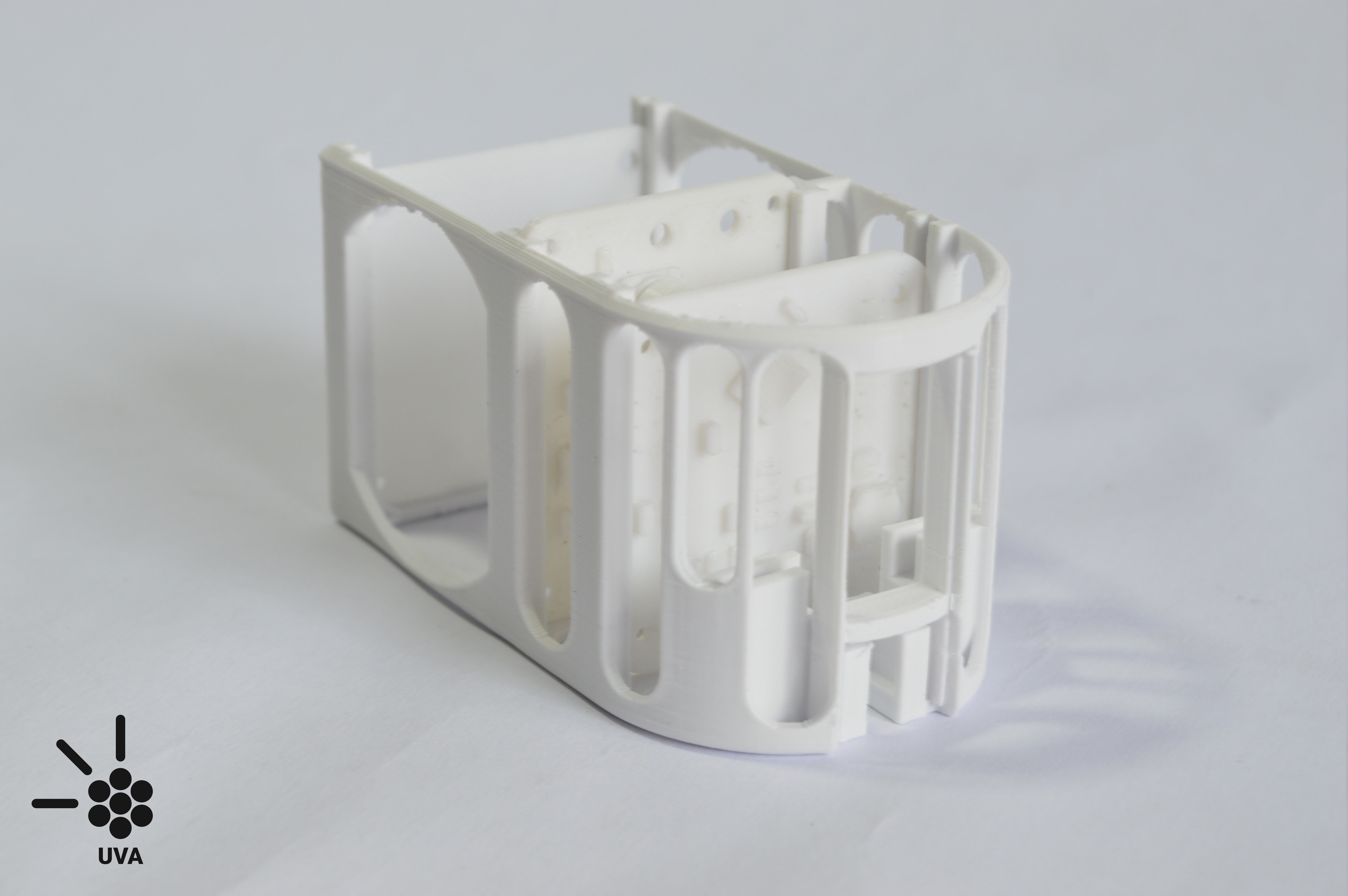
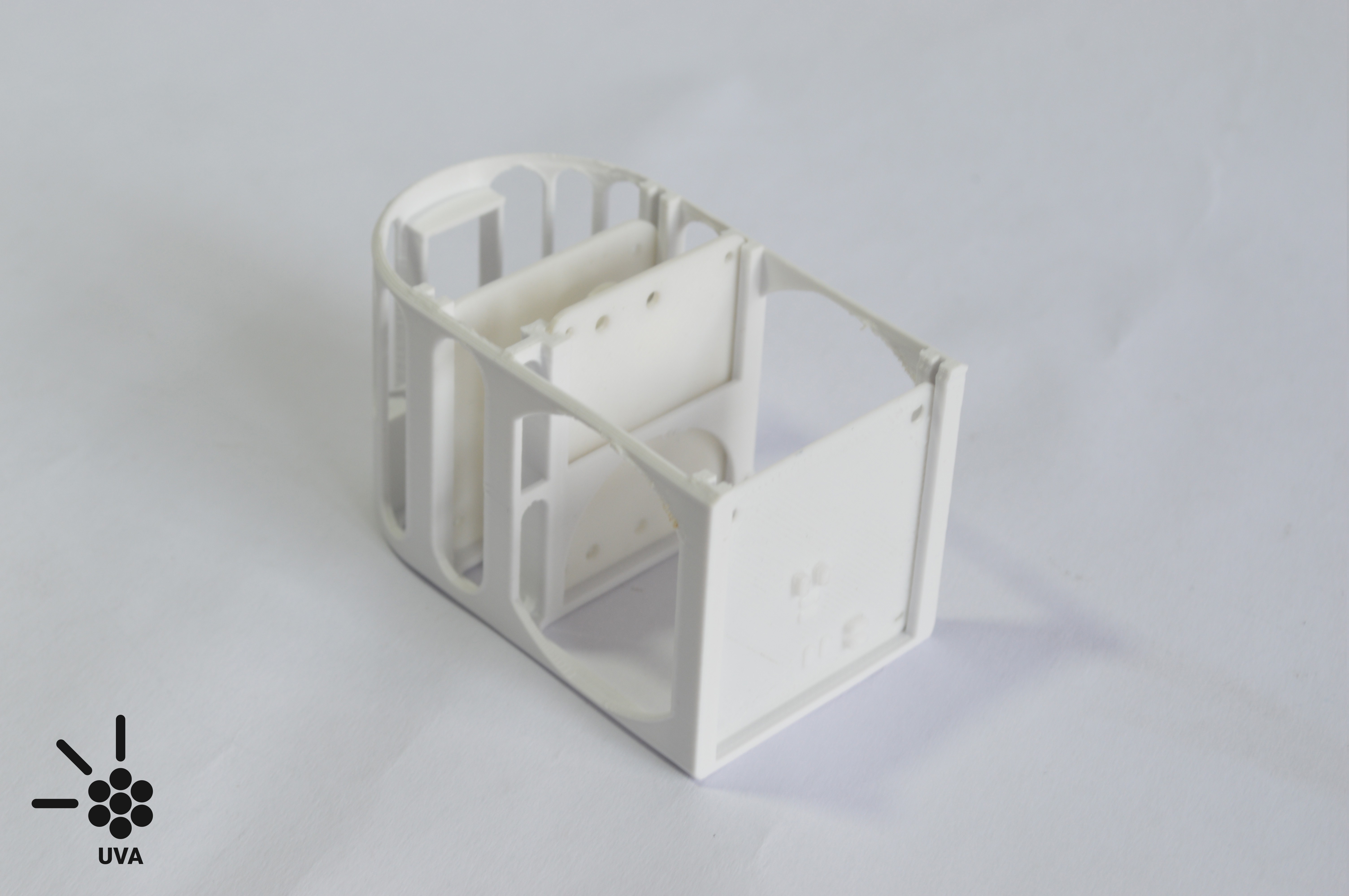
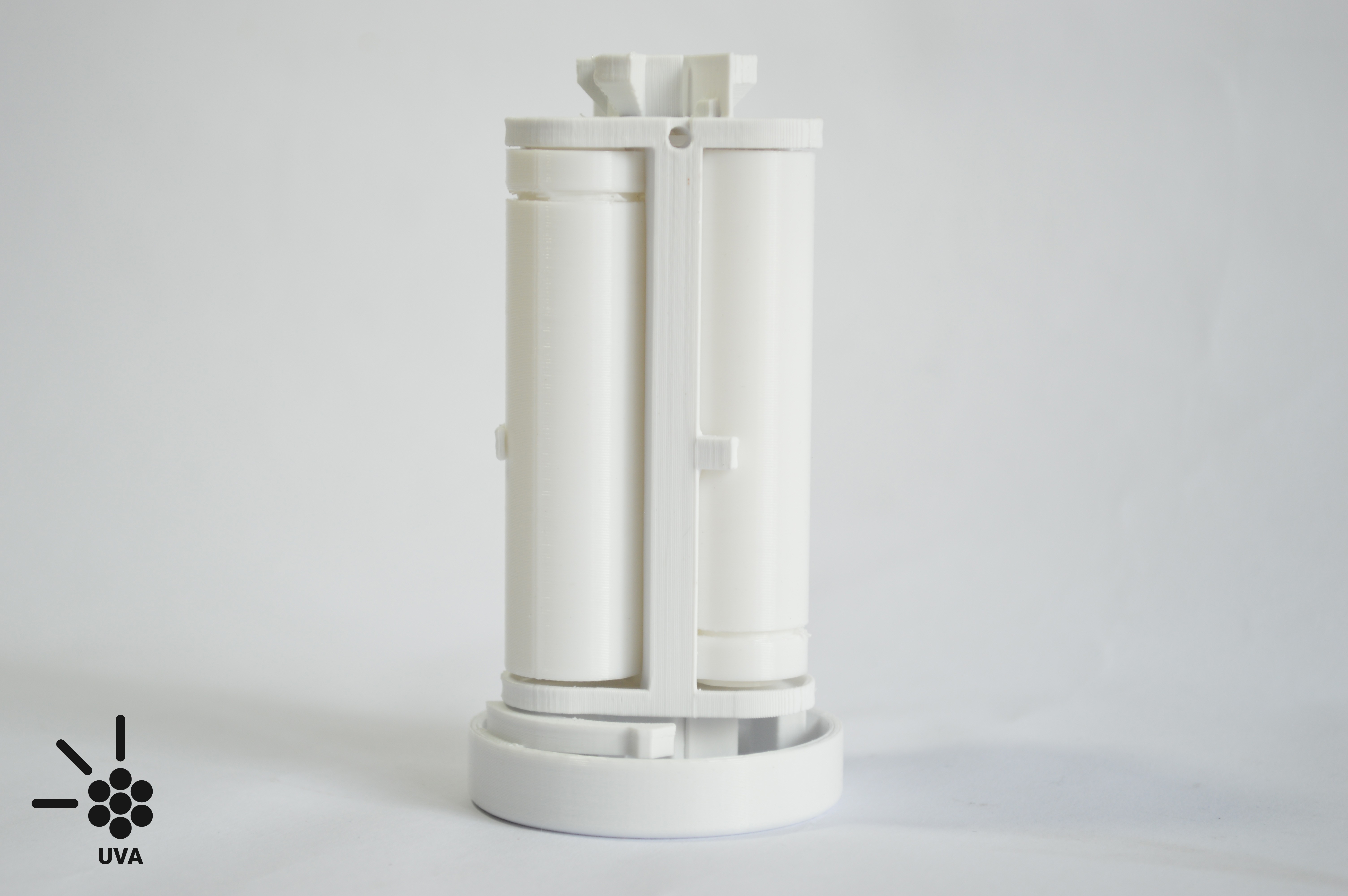
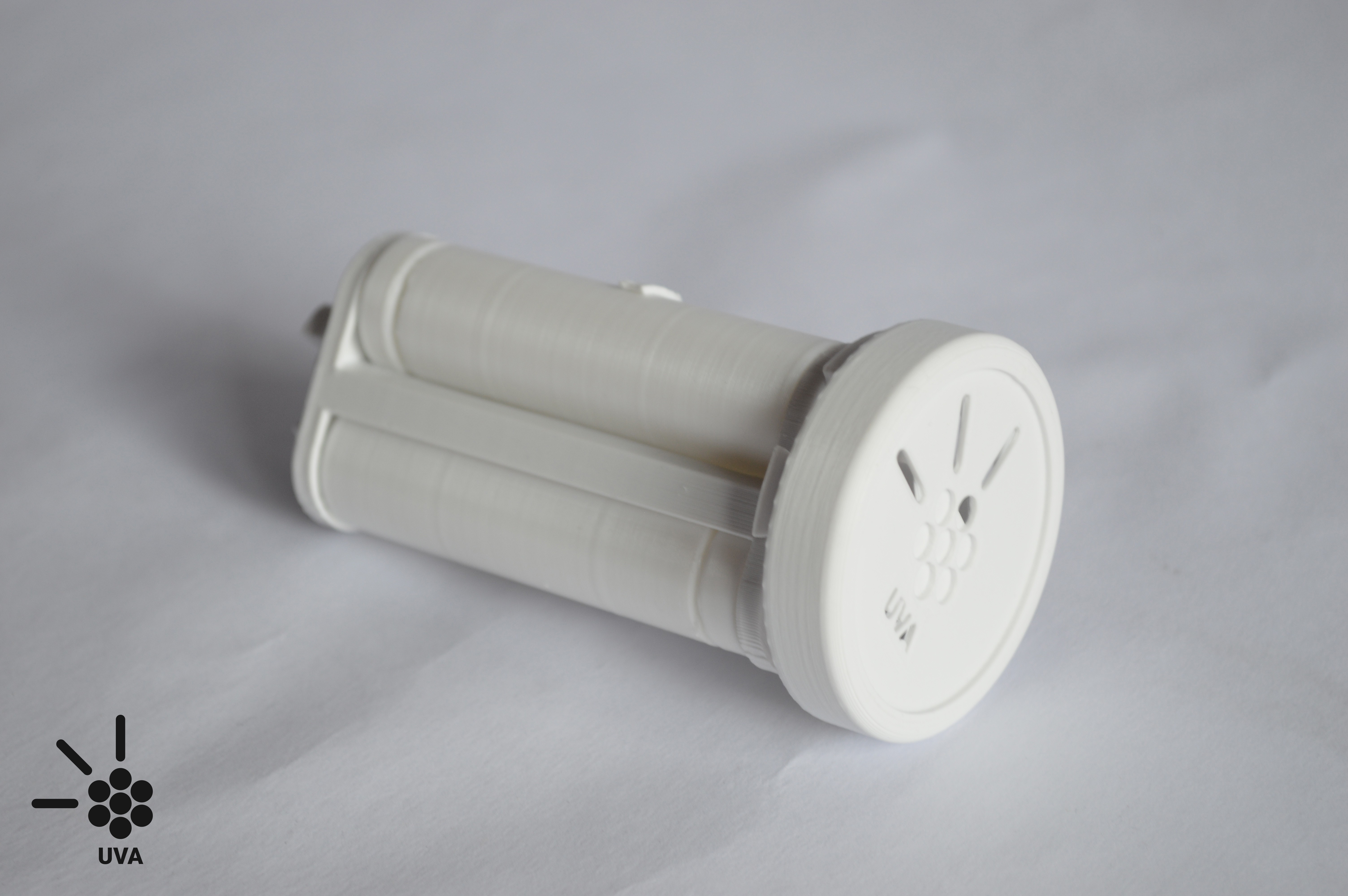
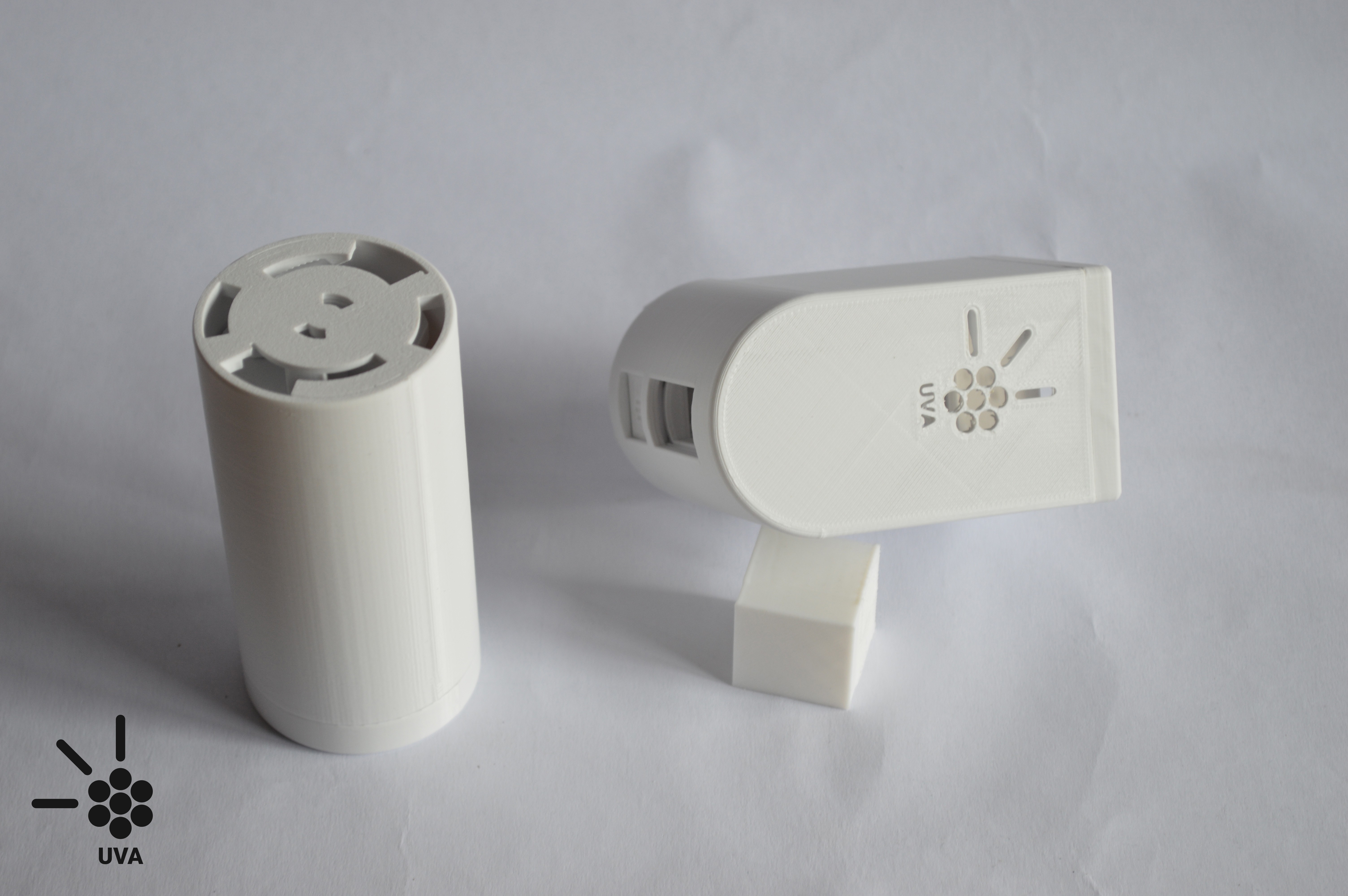
UVA Battery Pack
10/02/2020 at 13:09 • 0 comments![]()
Considering that we have created a multi-tool system with exchangeable tool heads, the battery pack is one of the core parts of the tool. In this case, we create a removable battery that connects to the tools with the UVA joint. It will be possible to integrate the changing module of the battery into the design of the battery pack in further iterations but, for this prototype, the batteries have to be charged in an outside charger.
The configuration of the battery is a 3s 1p of lithium batteries (Keeppower 18650 3500mAh protected), with a total voltage of 11.1V and a capacity of 3.5 Ah. UVA light is a high power-consuming tool because of the needs of UV-A light to cure the adhesives. Even so, we manage to have an estimated battery life of 1.5 hours of continuous use.
![]()
The batteries rack and UVA joint use the same contacts to transmit electricity, we select this one for the task (THM BATTERY CONTACT .545x.250) because was the one that adapts better to the design. Besides, because of the limited dimensions of the UVA tool, it was necessary to have a compact contact to manage the transmission of electricity to the tool head.
The battery consists of 3D printed parts (the rack, the case, and the bottom cap) and insight the battery pack we arrange 6 contacts for the 3 batteries and 2 contacts for the joint, also it is necessary some cable to joint the contacts from the batteries to the ones of the joint.
![]()
![]()
![]()
![]()
![]()
-
UI / UX
10/01/2020 at 06:08 • 0 commentsThis is one of the most exciting logs to write because, sometimes, makers and designers miss the whole point of a product. The main driver should be the satisfaction and comfortability of the final user.
UVA was designed with a balance between simplicity and functionality. Besides, we tried to create a neutral object that avoids rememorating anything like a firearm or something relatable to violence. This is because we believe that it is necessary to have in mind that the possible places where UVA could be used (for example countries with lots of violence, uncertainties, and war conflicts).
To address the user experience and interface we took in mind 5 main aspects:
- Fewer parts, fewer problems
- Modularity and replaceability
- Simplest functionality (one button)
- Only necessary information (the screen)
Fewer parts, fewer problems: UVA has a reduced number of parts for two main reasons. First, we wanted to reduce the risks of failure, and fewer parts are less possible corners of possible issues, it also helps in the replaceability. Second, because of the possible users of UVA, fewer parts makes the production and ensemble processes easier. Also, all the steps to build and ensemble UVA are designed to reduce the difficulty of creating a UVA.
![]()
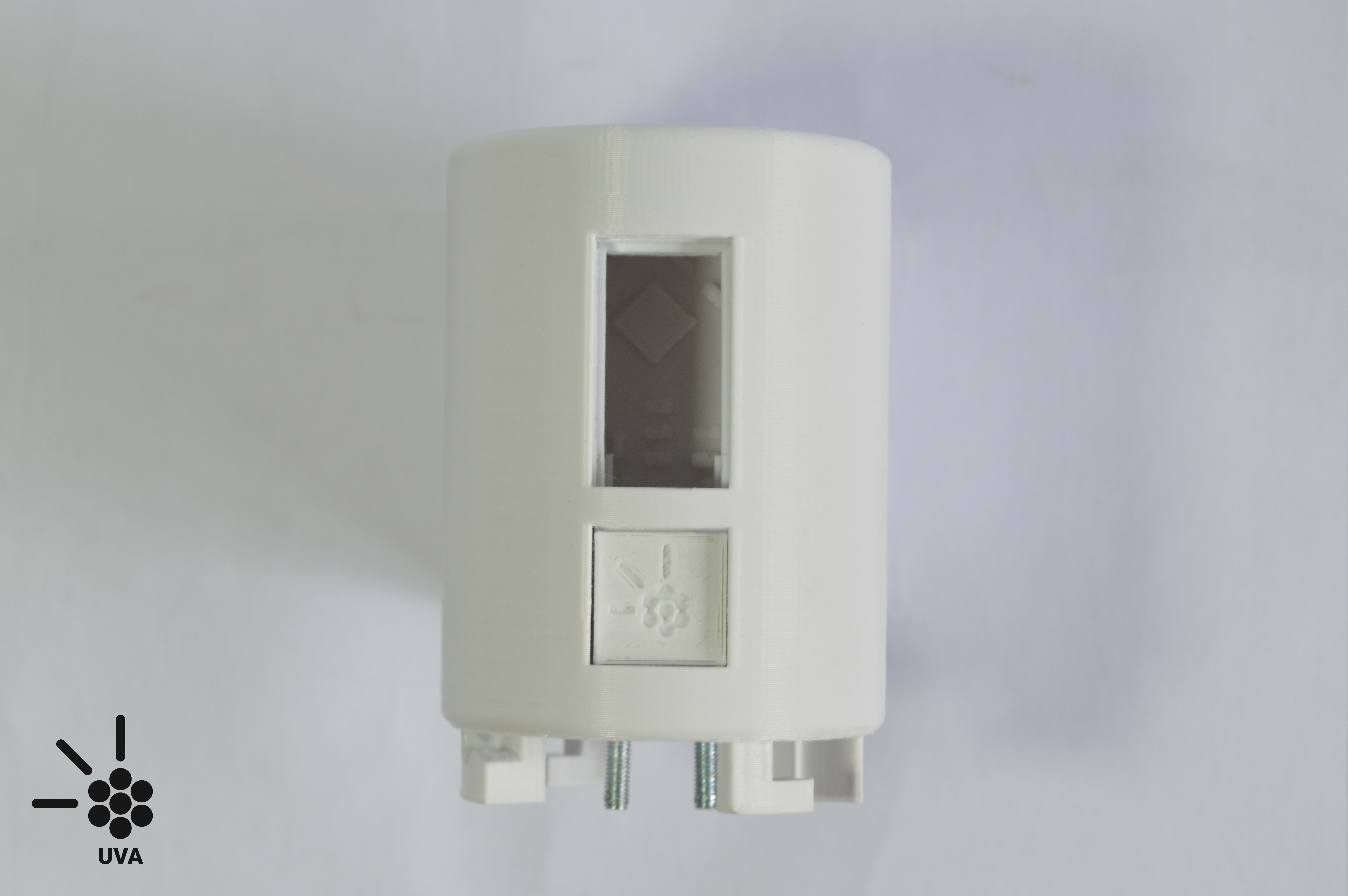
Modularity and replaceability: UVA is a modular design and it is separated into two main parts, the tool head, and the battery. Both the battery and the head host a holder for the electrical parts and circuits. It gives easy access to change batteries or replace a circuit board.
![]()
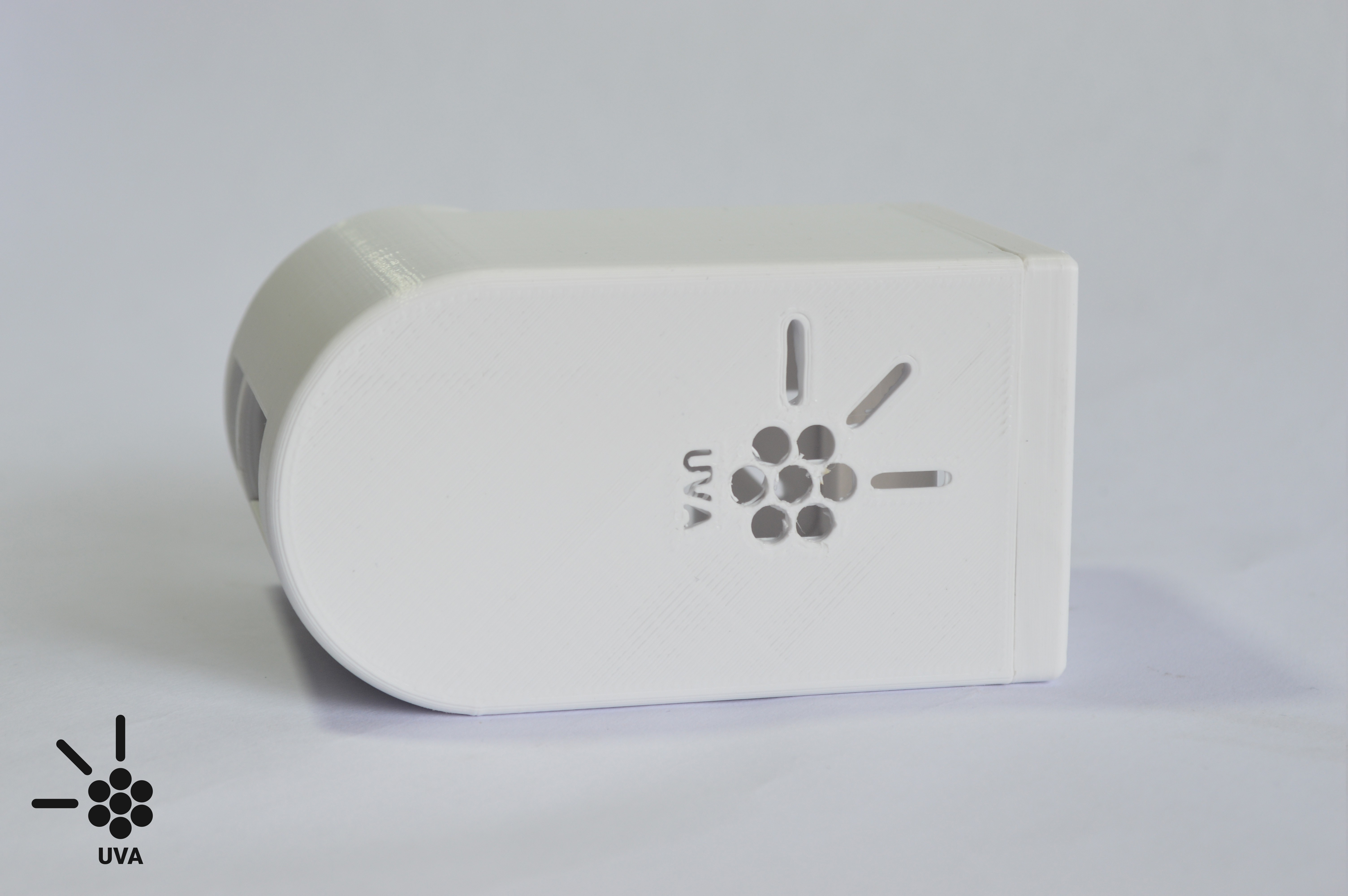
One Button: We wanted to create an object that was intuitive to use. So, we managed it, hopefully successfully, by adding only one button with simple functionality. If you press and hold the button UVA and the screen turns on and the chronometer and the distance measurement begging. When you release the button, UVA turns off and resets the screen and the chronometer.
![]()
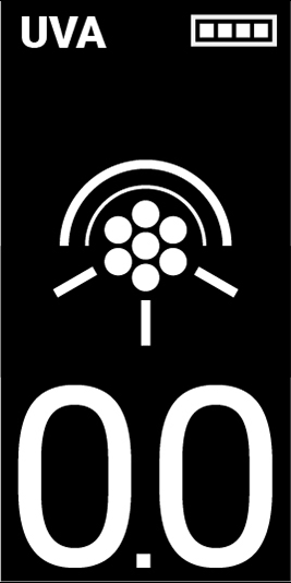
The Screen: we selected an OLED backlight screen because it allows working on low light environments. UVA screen has 3 main functionalities that will be shown only when you press and hold the button. It has a chronometer to measure the time that you are exposing the adhesive to the UV-A light (it is necessary a specific curing time for the UV Adhesives).
![]()
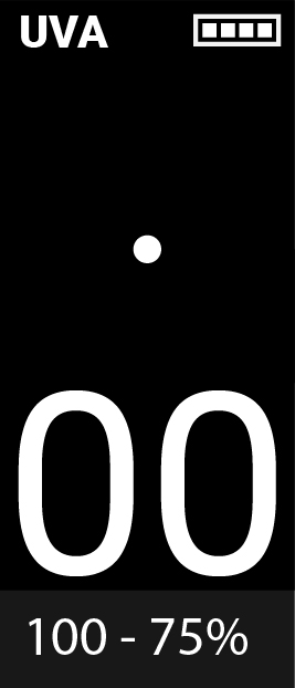
Then we have on the upper right corner the battery charge.
![]()
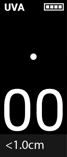
And last but not least, is the distance measurement and it shows distances between 0 cm and 15 cm, also with a signal at 7cm that is the optimal distance to achieve the maximum exposure to the UVA light.
![]()
Those are the main issues addressed by UVA considering the User interface and the user experience of the tool.
-
High-efficiency LED driver circuit
08/30/2020 at 21:16 • 0 commentsHaving previously decided which, and how many, LEDS we are going to use. It is now time to design a driver to power them. This post goes through the calculations needed to design the circuit, the following post gives some recommendations on designing the PCB.
Here is the final product.
26.4W Boost LED driver schematic 26.4W Boost LED driver PCB - 3D view Choosing the main driver IC
According to our calculations, to achieve max brightness we need a driver capable of providing 1Amp @ 26.4V (the combined forward voltage of 6 ls). Also, since our power source is a 3S Lipo battery, we need a BOOST driver, as the voltage provided by the battery 11.1v will need to be stepped up to the voltage required by the LEDs.
We chose the AL8553 because it has an external MOSFET, It's small, inexpensive, has good integrated over-current and over-voltage protections, supports dimming control through PWM, and comes in a leaded IC package (important for ease of soldering).
Taken from the AL8853 Datasheet Designing the Circuit
Designing switching converters is hard. Thankfully, the datasheet has all the instructions and equations required. Now, we only need to calculate the value of the components in the example schematics.
We are going to number the equations with the same numbers as the datasheet, so you can follow along if you want.
L1:
This is the main switching inductor of the circuit. Here's we need to calculate its Inductance and the Maximum Current it will handle. Here are the variables we know:
- Output Voltage: 26.4V
- Led Current: 900mA (To run the Leds at a little less than maximum power)
- Input Voltage: 11.1V (Nominal of a 3s Lipo battery)
- Efficiency η: 0.85 (Standard efficiency of BOOST drivers)
- Ripple Current Rate γ: 0.5 (Datasheet, p.10 suggest between 0.3 and 0.5)
- Switching Frequency f: 120Khz (According to datasheet p.4 table)
First we calculate the average current through the inductor:
Then the peak-to-peak variation of that current.
Now we know the maximum peak current that the inductor will need to withstand at any given point (And we can oversize it by 20% just to be sure):
Finally, we can calculate the inductance value like so:
Ok, so we know the inductor needs to be L1 = 43uH @ 3.8 Amps.Looking through Mouser, I found this one that I liked SRP1265A-470M (Link to mouser listing) from Bourns it's the exact same inductance value, but 47uH is close enough..
Inductor chosen for L1, picture from the Mouser Listing R6:
This resistor controls how much current goes to the LEDs. And, assuming a LED current of 900mA can be calculated with the following formula:
This resistor is in the path of the led current, so it's mportant to double check his power dissipation.
Therefore R6 = 0.222ohm @ 180mW
or if you prefer to run the LEDs at 1Amp, R6 = 0.2ohm @ 200mW
I liked the RCWE1206R220FKEA for the 0.222ohm, and the RCWE1206R200FKEA for 0.2ohm. They are high precision, and are rated for 0.5W of power.
Resistor chosen for R6, picture from the Mouser Listing R3:
This resistor controls the over-current protection trigger. The datasheet recommends setting this trigger point using 30% more than the maximum current expected by the circuit. Which happens to be the maximum peak current of L1, at the lowest expected Vin: 9v (The lowest safe voltage of a 3s lipo battery).
Using the equations from L1, we can calculate this peak current.
Finally, we over-size it by 30% to find the Over-Current Protection Current.
And now R3 is equal to:
We can also calculate the power consumed, just as we did with R6. Which means
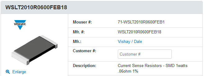
R3 = 60m @ 0.54W
That's a lot of heat for an SMD resistor, So it is important to size it appropriatly. I found the WSLT2010R0600FEB18 to be adequate for the job.Resistor chosen for R3, picture from the Mouser Listing R4 and R5:
This resistors are used in a voltage divider that sets the trigger for the over-voltage protection. Which is good to have in case the LEDs get accidentally disconnected during operation and leave the driver with an open-circuit. Mercifully, they have a fairly easy equation.
First, the datasheets suggests we define the Over-voltage threshold as 20% more than the nominal output voltage.
Now, the Relationship between R5 and R4 is given by.
Looking for a combination of standad value resistors that satisfies this ratio, I found a good pair with:
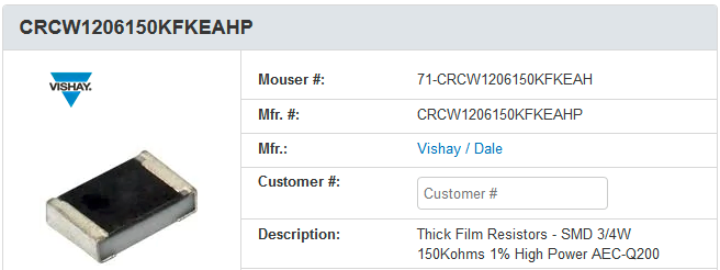
- R4 = 150K
- R5 = 10k
It is not an exact match, but it is close enough. These resistors don't need to dissipate a lot of heat, so it's critical which ones we choose. I liked these ones:
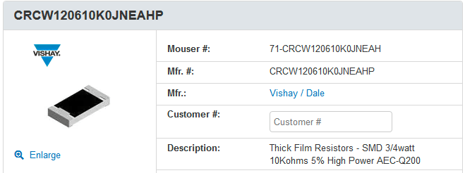
- R4 = CRCW1206150KFKEAHP
- R5 = CRCW120610K0JNEAHP
Resistor chosen for R5, picture from the Mouser Listing Resistor chosen for R4, picture from the Mouser Listing Q1:
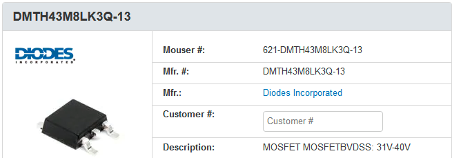
This is the main switching MOSFET. It only has a handful of recommendations on over specifying the voltage and current withstood by the transistor, namely
- Vds = 38.4V (20% more than over-voltage threshold)
- Ids = 4.63Amp (20% more than the nominal peak current)
- Vgsth < 13V (The datasheet p.4 says the max gate trigger voltage the chip can generate is 13V)
I searched around on Mouser and found the DMTH43M8LK3Q-13, which fits nicely with these recommendations.
MOSFET chosen for Q1, picture from the Mouser Listing D1:
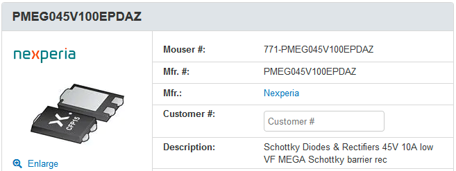
This diode also only has a handful of recommendations. It should withstand the same voltage as the MOSFET and as much current as the LEDs. Also, I personally recommend a Schottky diode, because the less the Forward voltage of D1, the less heat it will need to dissipate, and the more efficient the circuit.
Here is a good candidate: PMEG045V100EPDAZ, it has a nice Vf: 0.3V, which was about as low as I could find for this forward current rating.
Diode chosen for D1, picture from the Mouser Listing. R2:
This resistor controls the Slope Compensation features of the AL8853. However, we are not using this feature in this design, so this resistor is not necessary.
R2 = 0ohm.
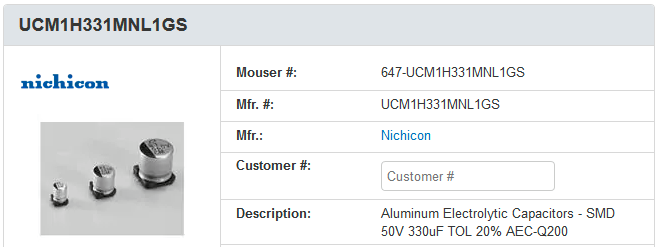
C3:
This is the output capacitor of the driver, it helps stabilize the output current. There are actually no suggestions of how to choose it. So, I took some inspiraton from some Texas Instrument Application Notes of high power LED drivers, and set it to:
C3 = 330uF @ 50V
I suggest this one UCM1H331MNL1GS. It has a high enough capacitance, and can safely withstand the output voltage.
Capacitor chosen for C3, picture from the Mouser Listing. C1:
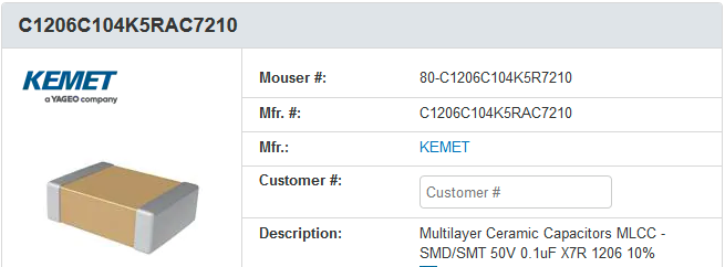
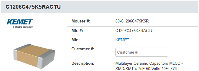
This is the Input decoupling capacitor, Also has no indications of how to select it. In this case we decide to use 2 capacitors in parallel:
- C1 = 4.7uF
- C4 = 100nF
These ones will work for this case: C1206C475K5RACTU, and C1206C104K5RAC7210
Capacitor chosen for C4, picture from the Mouser Listing. Capacitor chosen for C1, picture from the Mouser Listing. C2:
Funnily enough there is no mention anywhere of why this capacitor exists, or what it does. So I just chose this value and hoped it would work.
C2 = 100nF
I suggest using the same as C4.
Complete circuit schematic
Finally, we can put all this together, to get the full schematic
Full schematic of the LED Driver
In the next post, we will go into more details on how to design the PCB for this circuit. -
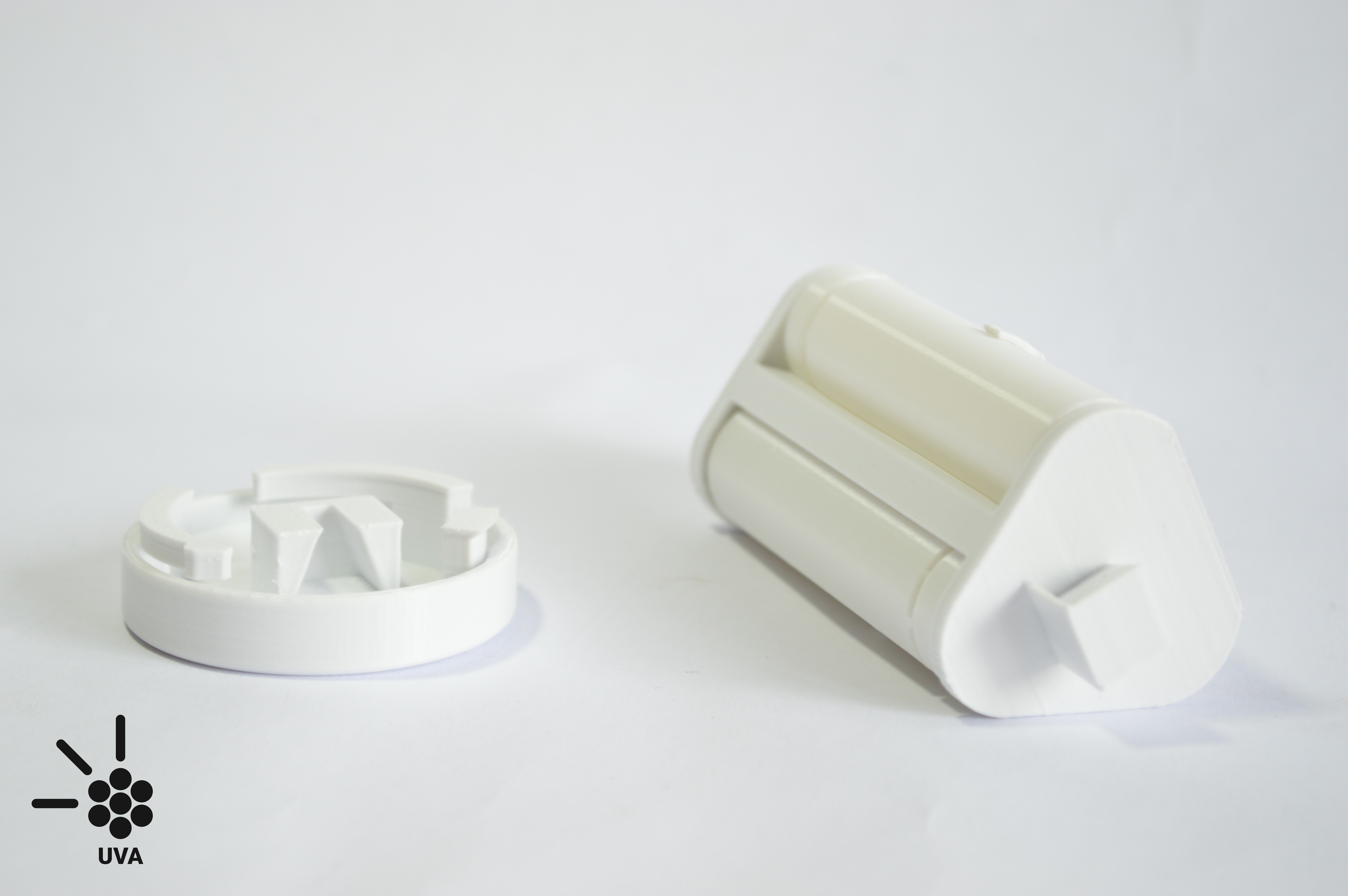
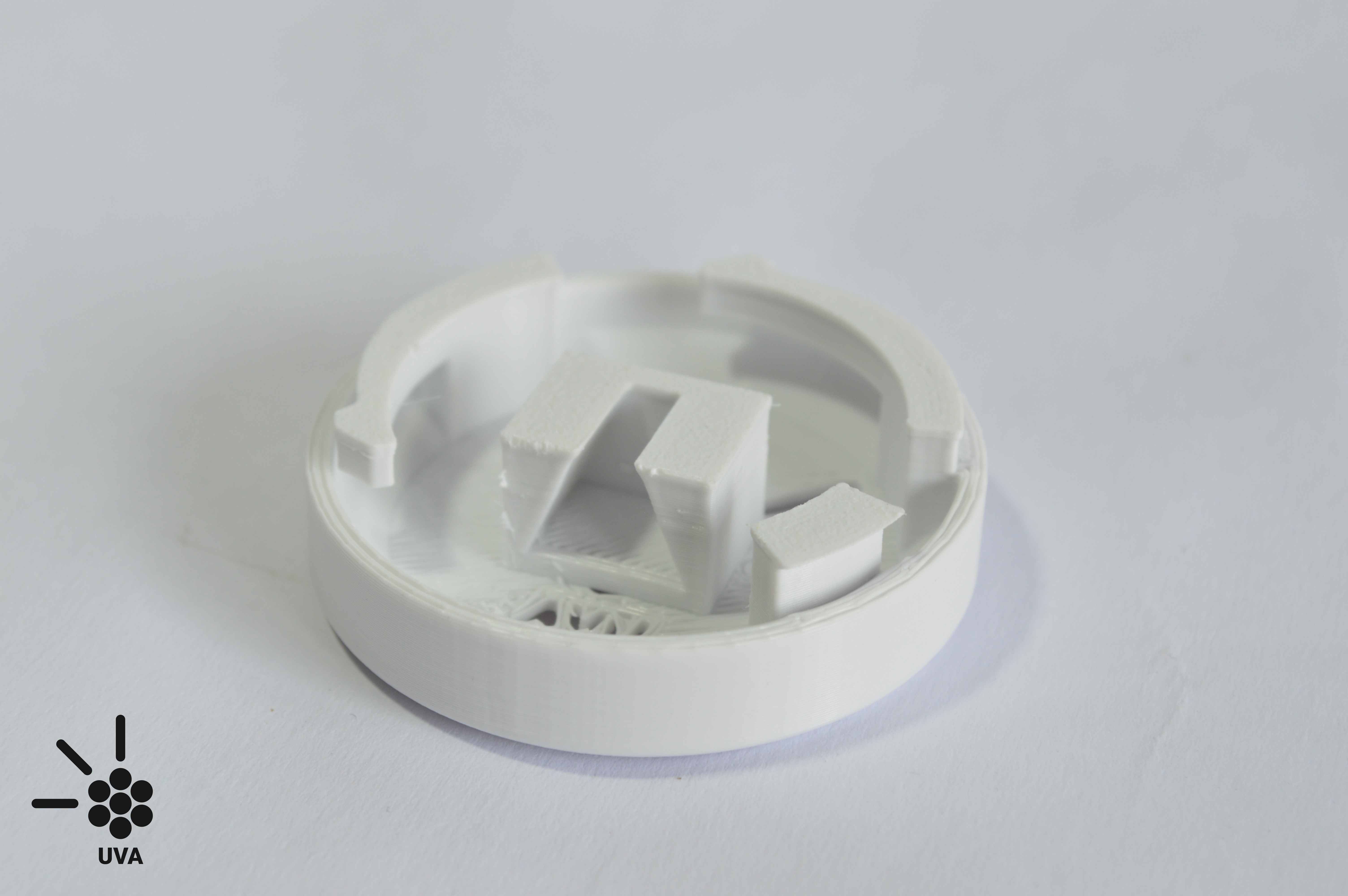
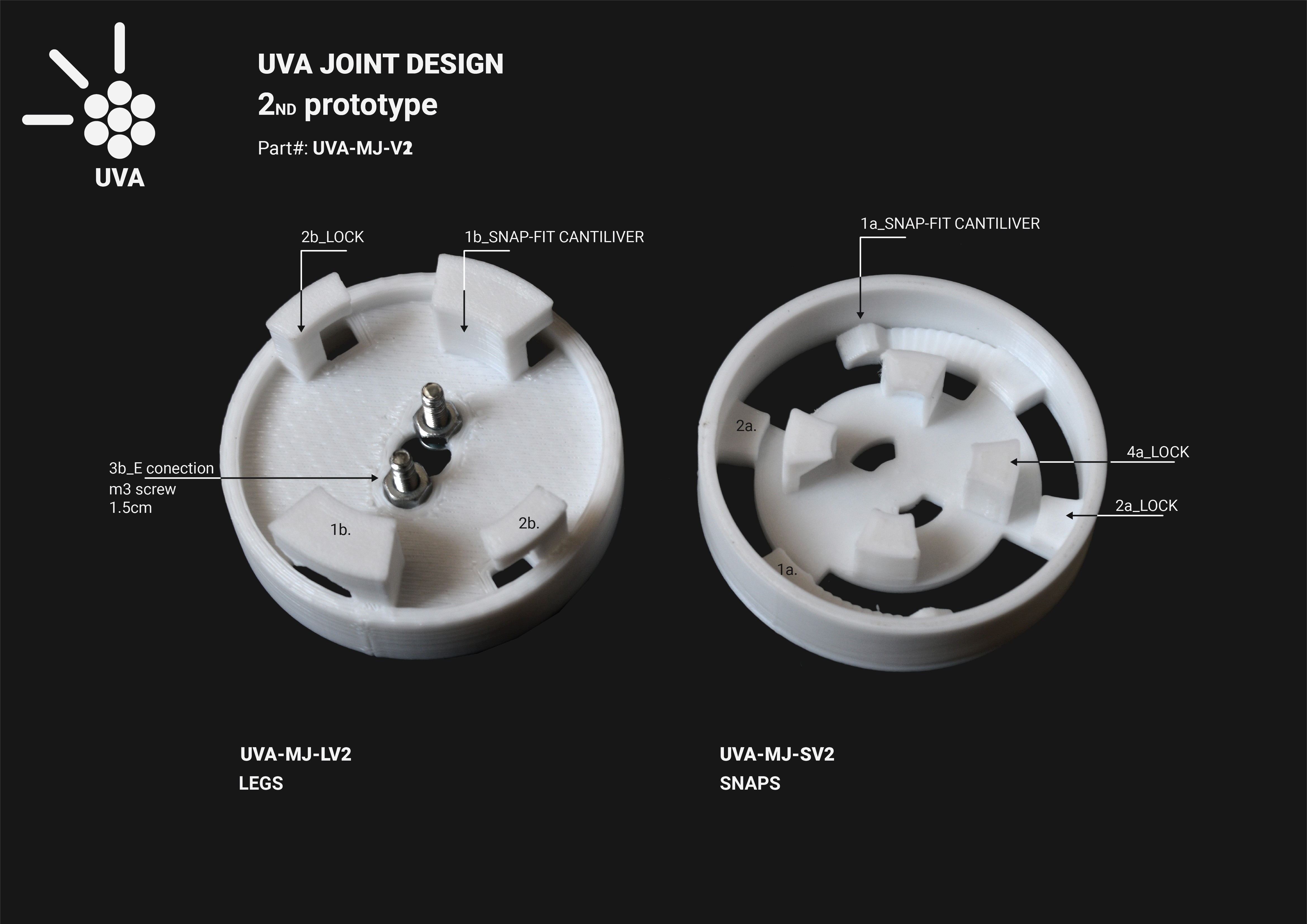
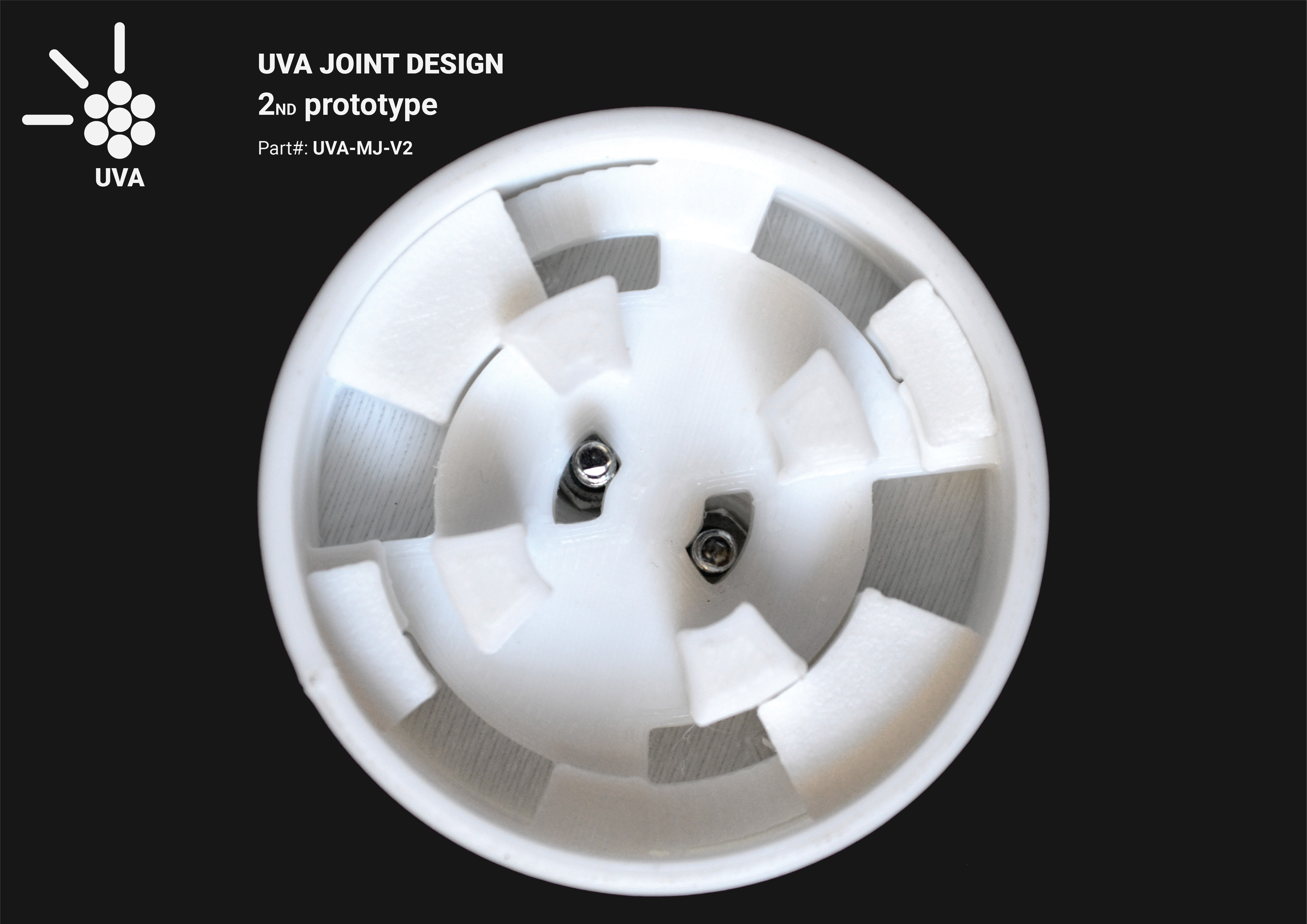
UVA Joint_V2
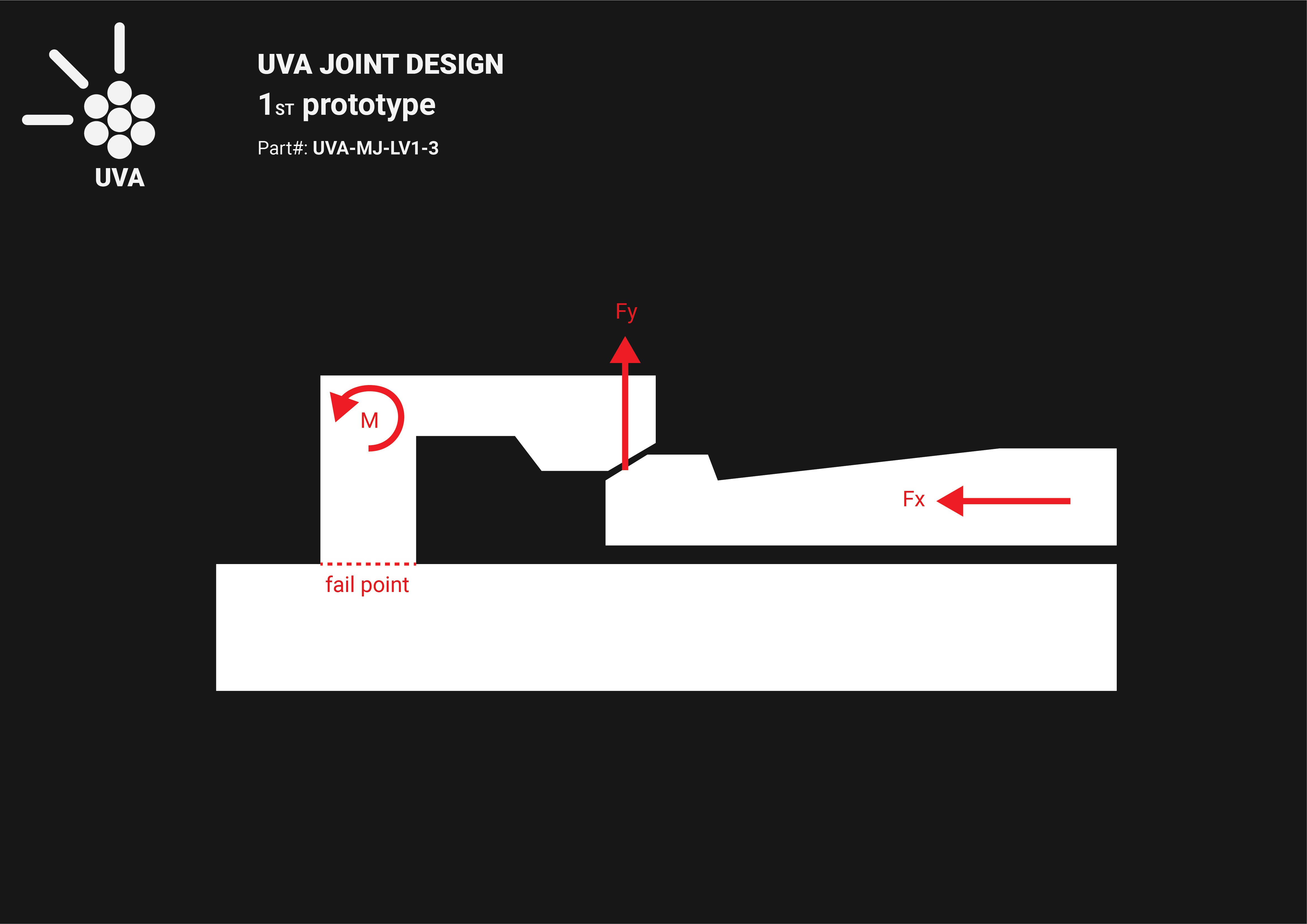
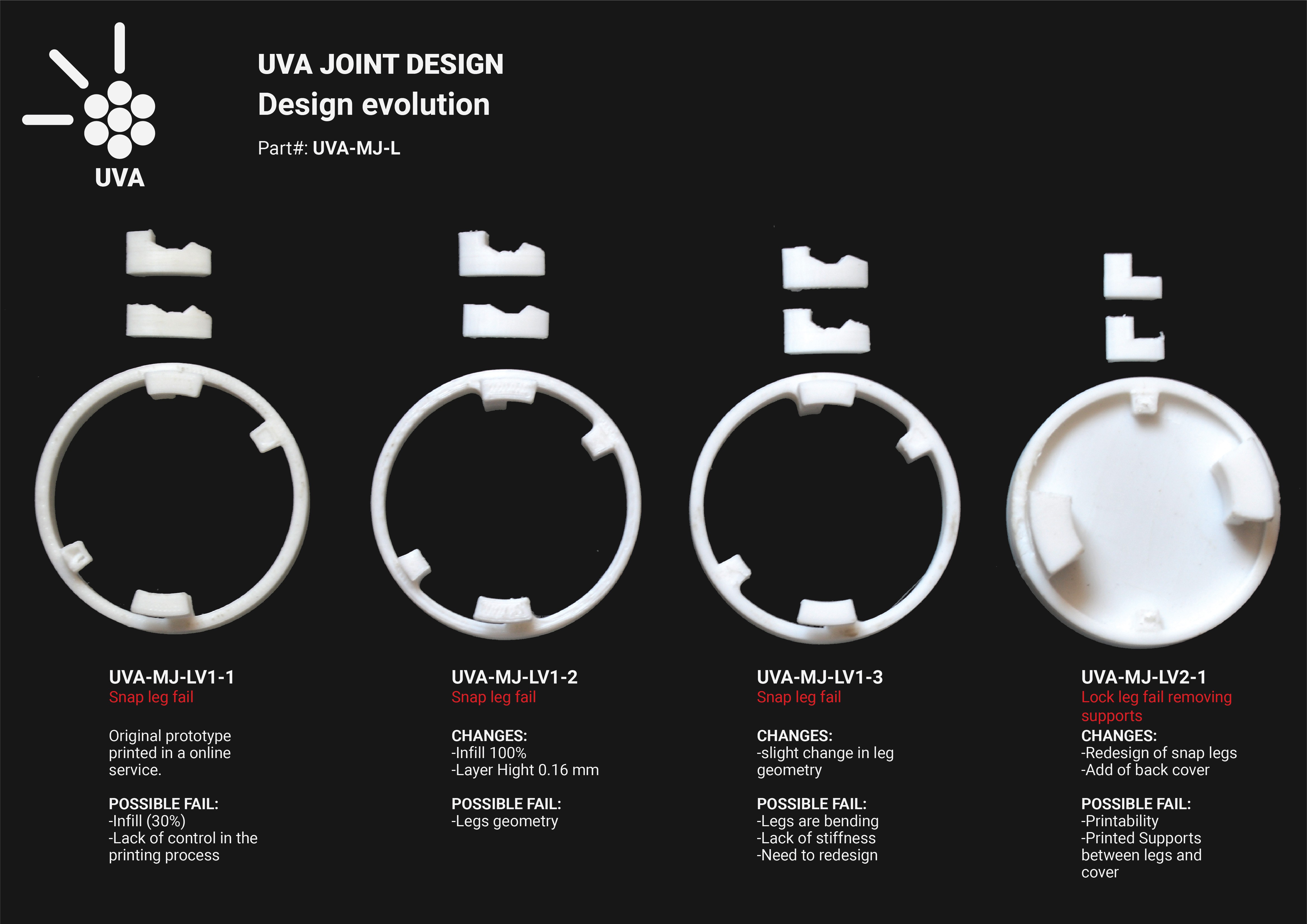
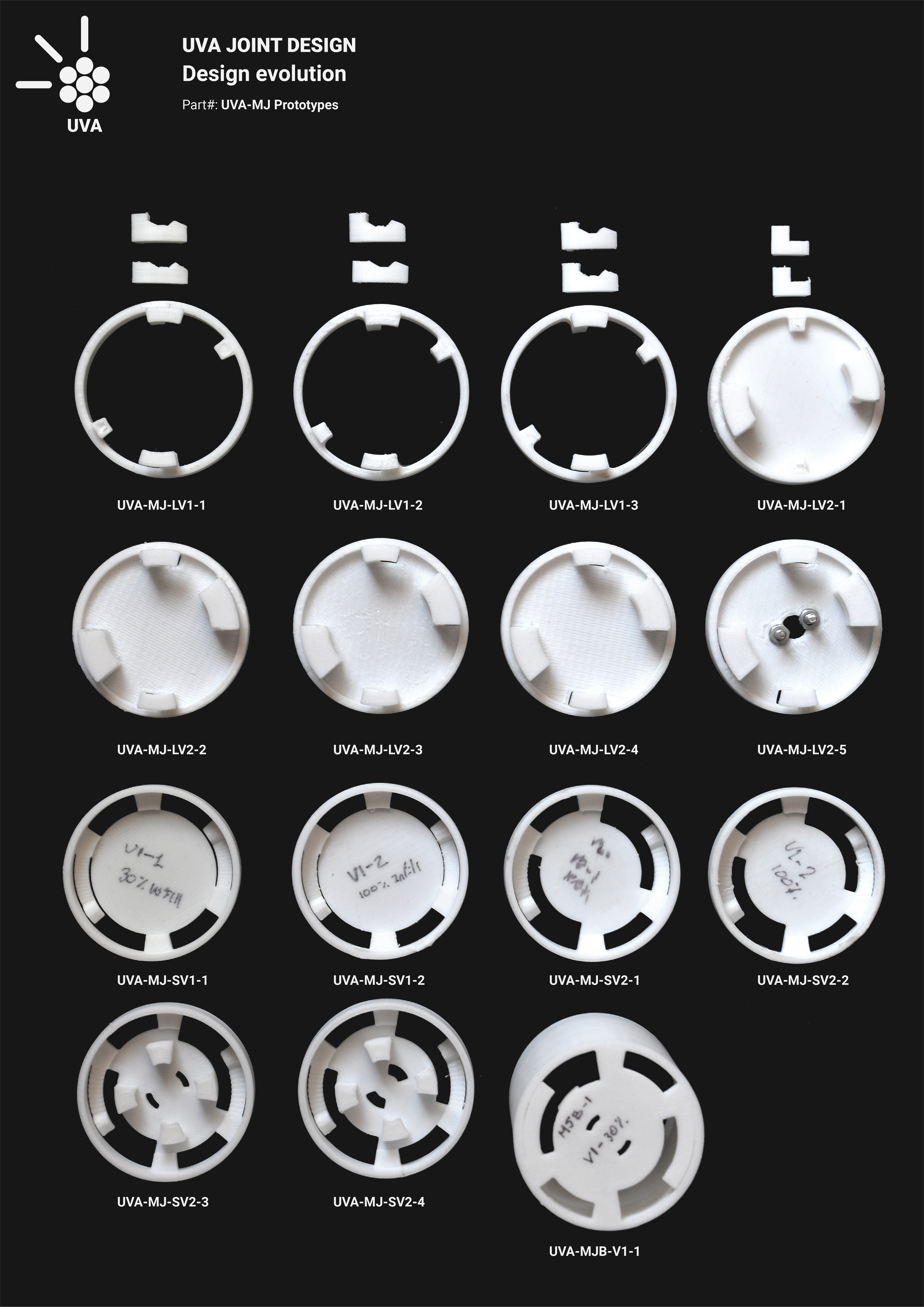
08/26/2020 at 16:32 • 0 commentsAfter a lot of tests and fails with UVA joint V1, we have developed a second version that solves the weaknesses of the first attempt. The main fail with the V1 was in the snap-fit cantilever connection in the legs ring (UVA-MJ-LV1_1b). This is the part of the joint that will be attached to the tool.

![]()
As you can see in the pictures it failed because of the lack of stiffness in the legs. The vertical force practised by the bending piece "1a" in the snaps ring at the moment of snapping also bent the legs in the legs ring. This part wasn't either design or prepare to bend. Because of the way that FDM 3d printed pieces work, the maximum flex and bend resistance is achieved parallel to the layers. In this case, the force applied to the leg was perpendicular to the layers and, after some attempts to connect both rings, the piece failed and break in the joint between the plastic layers.
![]()
![]()
![]()
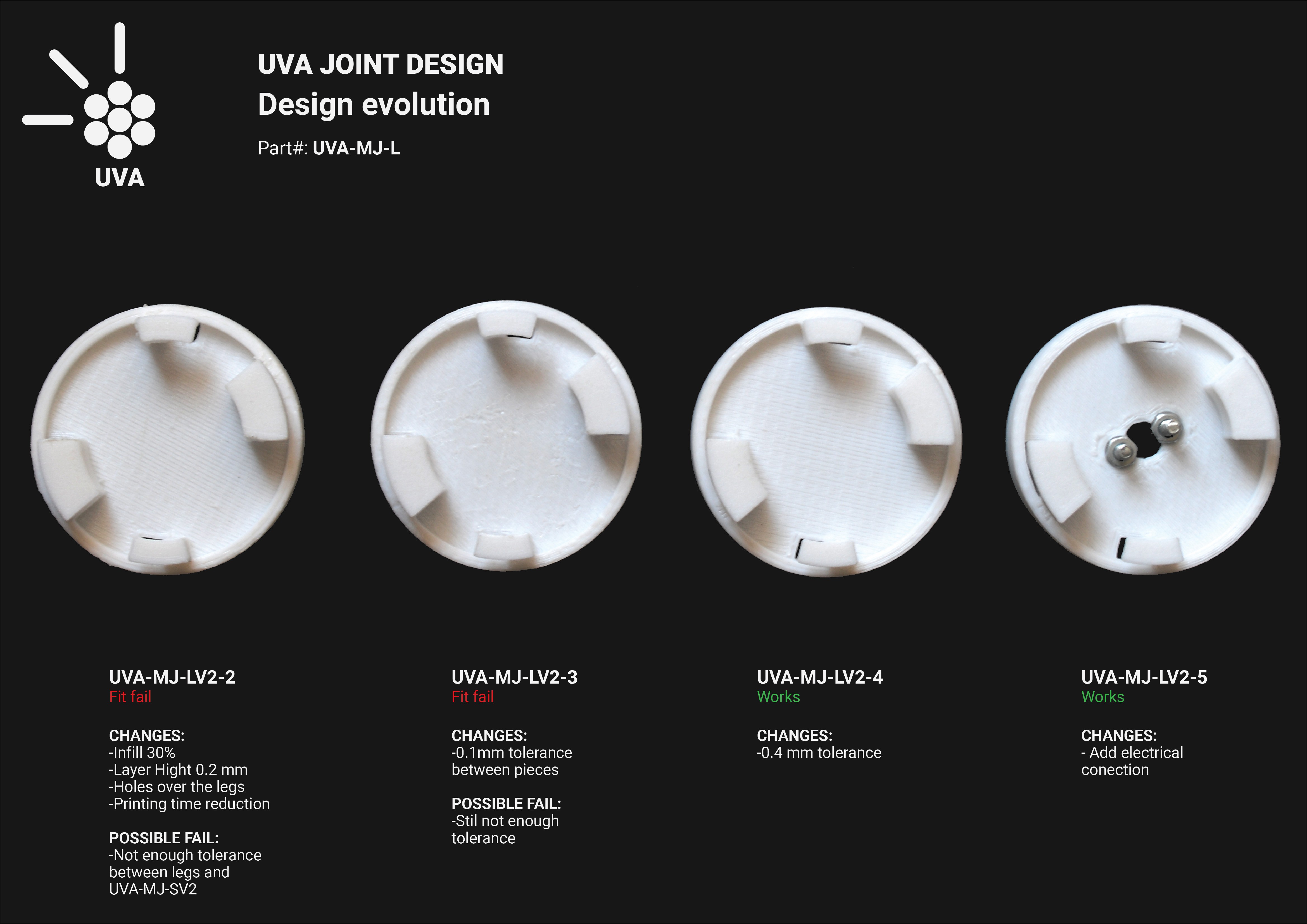
In the UVA Joint V2 (UVA-MJ-V2) we increased the area of the legs to achieve the necessary stiffness to prevent bending and also to increase the surface of contact between the layers. With the new solution came some new problems, mainly related to the printing process. The leg parts both snap-fit and locks have to fit in the snap parts with not too much tolerance to guarantee a good joint. So the termination of those has to be very precise and it is necessary to avoid supports to print the legs. As you can see, we left some holes over the legs to guarantee a qualitative termination.
Furthermore, we already took the next step and designed the electrical connection in the legs ring, and we are really close to finished the battery pack design but it will be discussed in another log.
![]()
![]()
UVA
High-power ultraviolet flashlight for curing UV adhesive (https://bit.ly/FldRdy-DB)