zpekic
-
Minor instruction set update
02/19/2024 at 06:44 • 0 commentsAfter writing some rudimentary assembler routines (with the idea of incorporating them later into a monitor type program), it appears that programming the SIFP is sometimes clunky, sometimes elegant. Lack or registers and absence true base + index addressing modes requires frequent stack saving and retrieving. On the other hand, each register having own flags, and parallelization of some operations in same instruction can offset that inconvenience. To improve the instruction set a bit I implemented following modifications:
- Added SBC (subtract with carry)
- Removed SLC (shift left through carry) - because I needed 1 opcode for SBC
- Renamed SRC to RRC (rotate right through carry)
SBC
SBC is same as 6502-type SBC, except 16-bit instead of 8. AC (accumulator carry) value 1 means "no carry". While XOR and then ADC can substitute SBC, it is inconvenient if one is to implement decimal arithmetic. I plan to do that for SIFC, exactly like 6502, by adding a D (decimal) flag.
D flag value 0 (binary mode) 1 (BCD mode) ADC - second operand no change no change SBC - second operand 1's complement (XOR with 0xFFFF) 9's complement Result Not adjusted BCD adjusted SLC
This was actually "RLC" (rotate left through carry), which can be replicated by this simple sequence:
PUSHA;
ADC, M[POP];
Given the infrequent use of this instruction, trade-off with SBC is probably good choice.
RRC
Only the name has changed, it always behaved like a Z80-style RRA. Accumulator and AC flag are treated as one 17-bit register (AC is LSB) and bits in it are rotated towards LSB.
The new instruction set table now looks like this:
![]()
CLRx
These instructions were always there and working, but I decided to "expose" them using the microcode compiler's primitive ".alias" pragma. From sifp.mcc :
// Convenient clear operations (internal data bus is 0 by default if not driven)
CLRA	.alias  r_p = NOP, r_a = LDA, r_x = NOX, r_y = NOY, r_s = NOS;
CLRX	.alias  r_p = NOP, r_a = NOA, r_x = LDX, r_y = NOY, r_s = NOS;
CLRY	.alias  r_p = NOP, r_a = NOA, r_x = NOX, r_y = LDY, r_s = NOS;
CLRAX	.alias  r_p = NOP, r_a = LDA, r_x = LDX, r_y = NOY, r_s = NOS;
CLRXY	.alias  r_p = NOP, r_a = NOA, r_x = LDX, r_y = LDY, r_s = NOS;
CLRAXY	.alias  r_p = NOP, r_a = LDA, r_x = LDX, r_y = LDY, r_s = NOS;
What is going on here?
Each register P, A, X, Y, S has only 1 input. This input is internal data bus, which gets its value by logical OR of all the registers that have output enabled. In case no register is "projecting" data, it the value of the internal data bus is 0. In the processor implementation this is visible here:
-- MUX to allow pushing, storing F to stack memory
int_fdbus <= reg_f when ((i_is_ftos or i_is_pushf) = '1') else int_dbus;

-- internal data bus is logical OR of all registers that project data
int_dbus <= p2d or a2d or x2d or y2d or s2d or d2d;
p2d <= p when (reg_p_d = '1') else X"0000";
a2d <= a when (reg_a_d = '1') else X"0000";
x2d <= x when (reg_x_d = '1') else X"0000";
y2d <= y when (reg_y_d = '1') else X"0000";
s2d <= s when (reg_s_d = '1') else X"0000";
When the internal data bus is 0, any register can pick up that value for a convenient "clear", which is somewhat common operation.
Inherent "superscalar" architecture allows any combination of A, X, Y to be cleared in one instruction. Some of these are exposed as aliases. It is also possible this way to clear P and S:
- clearing P - this is effectively jump to location 0, which is where execution start after RESET. I have not decided yet whether to use this as "soft reset" or maybe even "software interrupt"
- clearing S - this would destroy stack, therefore only useful during cold or warm restart.
-
Toolchain notes
12/19/2023 at 05:28 • 0 commentsTooling is one of the most important things in software engineering. Better tooling means better quality and productivity, and often security, documentation, list goes on.
The description below applies to this project but also other similar ones.
Build time
Two main tools are used:
- Microcode compiler. This is 2-pass command-line compiler I wrote in C# for all my micro-coded CPUs and controllers. For this project it was modified to:
- support alternative mnemonics (delimited by "bar" | )
- better #include processing (dynamic .org statements)
- various minor fixes
- Ancient Xilinx (now AMD) ISE 14.7 - obsolete, but still free and still works, sufficiently well for FPGA boards I mostly use.
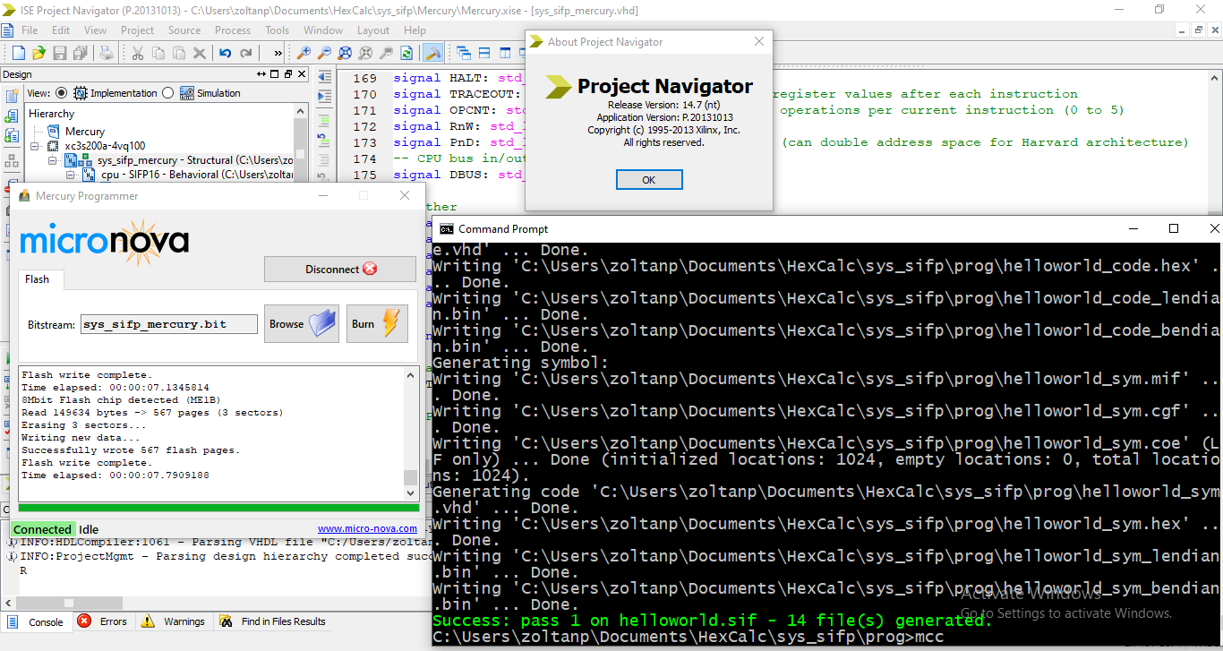
Microcode compiler consumes .mcc or .sif text source files and can generate various output formats, for example Intel .hex or .vhd. Either of these can be used to prime the "ROM" memory of the system.ISE14.7 - in addition to project files, also includes either .vhd produced by mcc or during build time loads the .hex file using a helper function.
The output is a .bin file which gets downloaded to the target device (FPGA board) using a utility tool.
![]()
Run time
Currently, system build around SIFC processor implements:
- VGA (32*64 character only) as primary output device
- UART (bi-directional, connected to USB2UART device appears as COM: port) as "console" device (text-only input and output)
- UART (one-directional, connected to USB2UART device appears as another COM: port) trace output device
There are two devices inside the target system that help with debugging:
- CPU which can be in trace mode (outputs register values) or non-trace. In addition it can be run with frequency 0 (single - step) to 25MHz
- Debugtracer which can intercept any bus cycle and "freeze" the CPU until that bus cycle data is output on the serial COM port (#3 above)
debugtracer mods \ CPU mode TRACEON TRACEOFF Enabled Allows tracing all bus cycles (except INTA) Allows tracing instruction fetch and memory read/write only Disabled Slow system speed (8 clock cycles per instruction) Full system speed (2 clock cycles per instruction) On the host PC, COM port #2 must be connected to some terminal emulator type of application to allow command interaction with the system.
However, for COM port #3, there are 3 options:
- do not connect (ignore trace output even if present)
- connect to terminal emulator app (and observe raw trace output)
- start tracer system tool (command line, written in C#) - it will take over the COM port and use trace output it intercepts to look up and highlight symbolic code, update memory map etc. Tracing can be stopped / restarted by "space" key on host which flips RTS pin on COM: ports which is picked up by the tracer. Symbolic breakpoints could be implemented using this capability in the future.
![]()
![]()
- Microcode compiler. This is 2-pass command-line compiler I wrote in C# for all my micro-coded CPUs and controllers. For this project it was modified to:
-
P, A, X, Y, S: more than a just another register
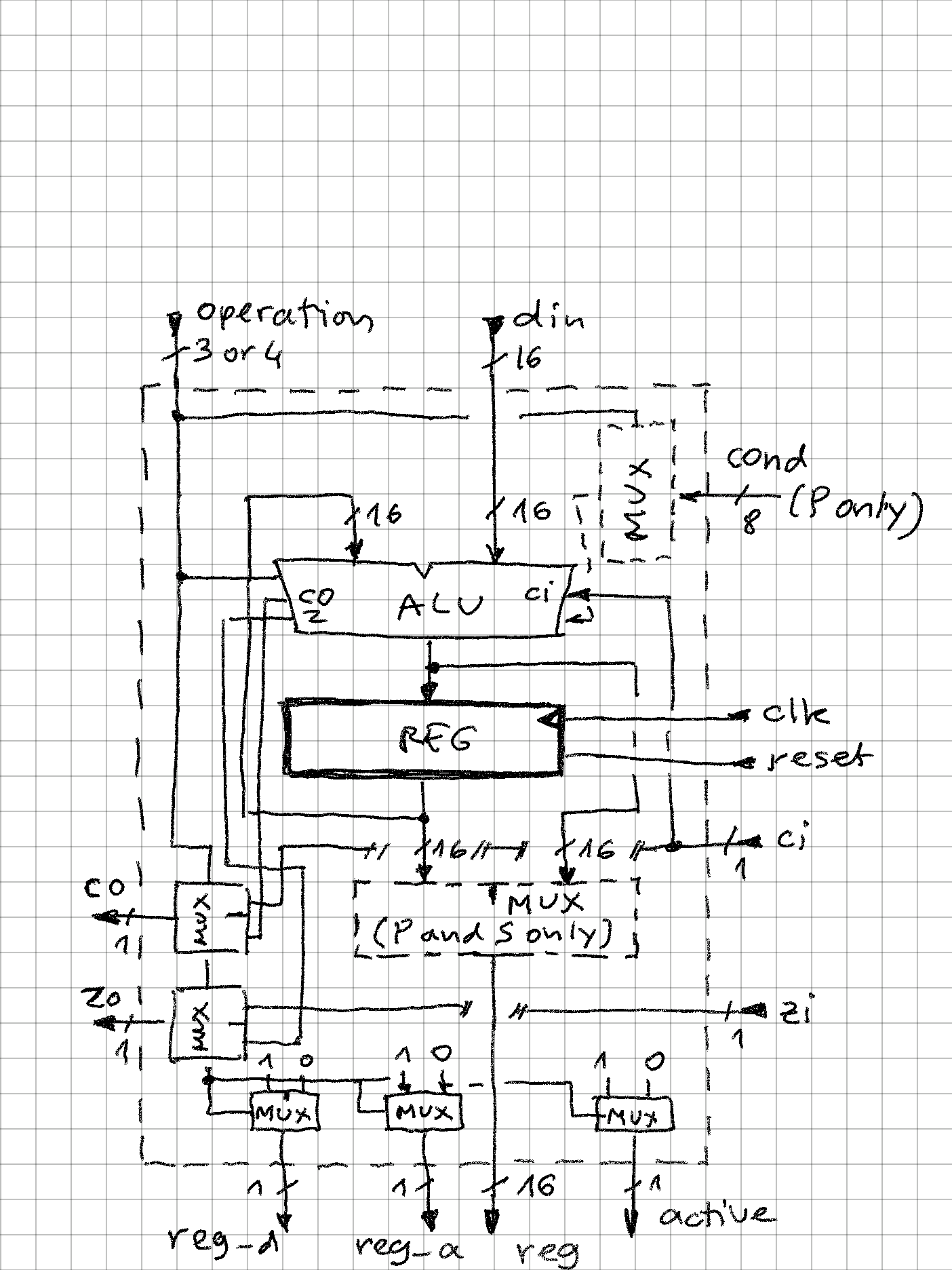
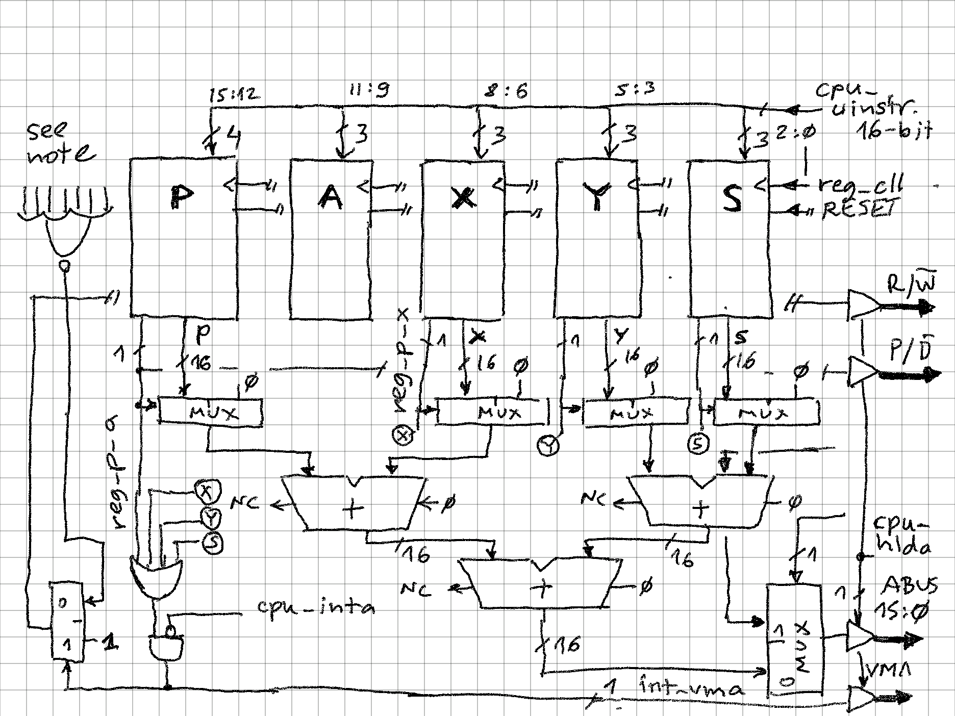
12/13/2023 at 06:50 • 0 commentsMost CPUs contain some number of internal registers, a subset of which are available for programs to use. These are often not much more than very fast internal memory connected to internal bus(es) and ALU(s), meaning that the the transformation of bits crucial for program execution is happening elsewhere and not within logical confines of the register.
SIFP-16 somewhat extends the concept of register to a "processing element" - each of these in addition to fast value storage is also given own simple ALU, flags inputs and outputs, as well as part of control over CPU data and address paths to make it a self-contained unit of data processing.
All 5 processing elements present in SIFP-16 have the following basic internal structure:
![]()
Main elements:
- 16-bit data value, "register", loaded with rising clock signal which is connected to all others PEs, and reset with also common reset signal (only for P and S is reset of importance as CPU boot depends on both being initialized to 0)
- operation - 3 or 4 control bits, selecting 1 of 7 or 1 of 15 operations (1 is always NOP). These are coming directly as a slice of the currently executing instruction code.
- single data input
- single data output
- carry and zero outputs, which depending on operation can be "passthrough" or coming from ALU
- control output signals reg_d, reg_a that drive the address and data paths
- control output signal "active" which is 0 only when operation is NOP. These signals are used to count CPU throughput, how many operations can be executed in single operation (min = 0, max = 5)
- register is updated through the ALU, which is in most cases a simple binary adder with some passthrough (e.g. NOP is always implemented as register reloading self-value)
- (optional) output MUX is needed as different value than register should be sometimes projected out (e.g. S + 1 before the value is updated)
- (optional) condition codes fed into P (program counter) branch / no branch decision logic.
Processing element operations are declared in the include file that defines the instruction field bits. This way the microcode source becomes a CPU assembly source file, and assembly instructions can use:
- any variation of the operation mnemonic (these are delimited with |)
- "aliases" which are handy shortcuts for most frequently used operation combinations (such as PUSH/POP etc.)
- each assembly instruction must be closed by ; but it can contain 1-5 operations and those must be delimited with ,
All program control depends on the operations that P supports. It is important to note that at time of execution of these operations P has been incremented and is pointing to next location in program memory, which can be used either as data (destination for jump, branch offset, immediate) or next instruction.
- STPx - because there can be no push and jump in same instruction (that would require 2 memory cycles and only 1 is possible), these allow to push "forward" P value to internal data bus
- JUMP|GOTO - allows use of absolute targets, for example system calls in ROM
- BRANCH - relative jumps can reach any target in the memory, but if confined to same module can implement relocatable code
- LDP - beside return, this operation allows jumping to location in any other processing element or memory pointed by it (e.g. LDP, X; LDP, M[Y]; etc.). This allows data driven "case" statements or dispatch tables.
// 16-bit program counter (has no flags, always increment during fetch phase, changes as below during execute phase) r_p .valfield 4 values NOP, // continue (increment P during next fetch phase) M[IMM], // output value as address, increment (used for immediate values) BRANCH|IF_TRUE, // unconditional branch (add word pointed by P) JUMP|GOTO, // unconditional jump (load with word pointed by P) LDP, // load from incoming data (mostly from stack, for return) STP4, // put P + 4 to internal data bus STP2, // put P + 2 to internal data bus STP, // put P to internal data bus (mostly to output during trace mode) BAC|IF_AC|IF_A_GE, // if A flag C set add word pointed by P (branch), else increment P BAZ|IF_AZ|IF_A_EQ, // if A flag Z set add word pointed by P (branch), else increment P BXC|IF_XC|IF_X_GE, BXZ|IF_XZ|IF_X_EQ, BYC|IF_YC|IF_Y_GE, BYZ|IF_YZ|IF_Y_EQ, BSC|IF_SC|IF_S_GE, BSZ|IF_SZ|IF_S_EQ default NOP;With only 5 remaining operations (after no-op, load and store are used), the dilemma was which others to implement:
- No subtract, because it can be implemented with XOR (negate bits) and ADC
- No OR because it can be done by driving the internal data bus with more than one source (for example LDA, X, M[Y] is equivalent to A <= X OR M[Y])
- No rotate because it can be (with some inconvenience) achieved with shift
- No compare, as equality comparison can be done with XOR, and magnitute comparison with various tricks (e.g. adding the negative value of the constant)
// 16-bit accumulator (has own carry (AC) and zero (AZ) flags, changes only during execute phases)
r_a	.valfield 3 values
	NOA,	// no operation on A register
	XOR,	// logical xor with incoming data (AZ)
	SLC,	// shift left through carry	(AC, AZ)
	SRC,	// shift right through carry (AC, AZ)
	LDA,	// load with incoming data (AZ)
	ADC,	// add incoming data and carry flag (AC, AZ)
	AND,	// logical and with incoming data (AZ)
	STA|A	// output value as data
			default NOA;
X, Y (index / base pointers / counter)
These two are identical in every way. Main uses are indirect and base + index addressing, counters, temporary storage.
// 16-bit index register X (has own carry (XC) and zero (XZ) flags, changes only during execute phases) r_x .valfield 3 values NOX, // no operation on X register CPX, // compare with incoming data (XC, XZ) INX, // increment by 1 (XC, XZ) DEX, // decrement by 1 (XC, XZ) LDX, // load with incoming data (XZ) ADX, // add incoming data (XC, XZ) M[X], // output value as address STX|X // output value as data default NOX;A very "classic" stack pointer, growing from high address towards lower. However the S points to TOS (top of stack) not the first free location on stack. So M[S] allows direct read and modification of the TOS. It is initialized at 0 after RESET, so first push will write to location 0xFFFF which is expected to be RAM (ROM is expected at 0x0000, i8080 style)
ADS and LDS allows (with some difficulty) implementation of stack frames and overflow checks.
// 16-bit stack pointer S (has own carry (SC) and zero (SZ) flags, changes only during execute phases)
r_s	.valfield 3 values
	NOS,	// no operation on S register
	CPS,	// compare with incoming data (SC, SZ)
	M[POP],	// address is S, then increment
	M[PUSH],// address is S - 1, then decrement
	LDS,	// load with incoming data (SZ)
	ADS,	// add incoming data (SC, SZ)
	M[S],	// output value as address (use to access stack top in memory)
	STS|S	// output value as data
	default NOS;
Processing elements recap:
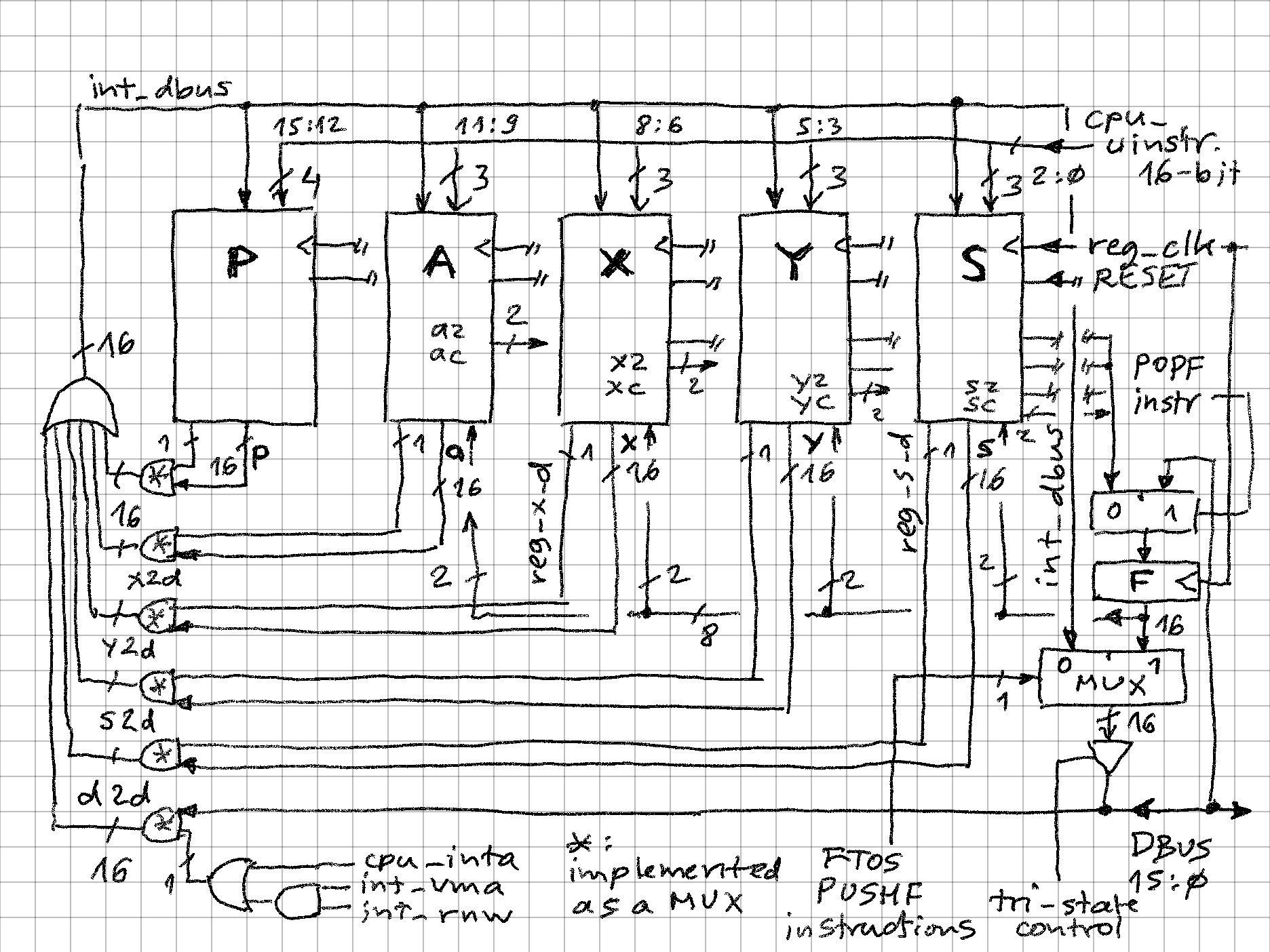
Processing element Instruction bit field Number of instructions Flags (carry, zero) Project data Project address P 15..13 16 (only consumes flags from A, X, Y, S) yes (multiple) yes (multiple) A 12..10 8 ac, az yes no X 9..0 8 xc, xz yes yes Y 6..4 8 yc, yz yes yes S 3..0 8 sc, sz yes yes (multiple) -
Datapath: circle more, bus less
12/12/2023 at 08:06 • 0 commentsCPU internal data paths come in many topologies and complexities - from simple bidirectional bus all the way to n*m matrix switches and everything in between.
SIFC16 datapath mostly resembles a circle, in the sense that outputs of all registers end up as inputs of these same registers:
![]()
There are also a few side loops along the way (for external data bus and F (flag register). Signal names are same like in the implementation, for easier following.
Reading data (from registers or memory)
Each of the registers (P, A, X, Y, S) generates two signals:
- 1-bit data output enable, which depends on the operation
- 16-bit data (register value)
For example index register X (and Y):
-- value
reg <= r;

-- projecting as data
reg_d <= '1' when (operation = r_x_STX) else '0';
So if reg_x_d is 1 (in case of STX or STY operations), then then "and" gate (which is actually a 32 to 16 MUX) will pass the value along to be combined in a OR gate array (16 OR gates, each 6 inputs wide, seen on center left):
- 5 inputs of the OR array are gated register values
- 6th input comes from DBUS (memory data bus). This input source is passed through if:
- interrupt vector is being read (cpu_intr control signal) - OR -
- memory address is valid (VMA = 1) and "read" mode (RnW = 1)
The combinatorial logic above drives the 16-bit internal data bus (int_dbus) which is then fed back to each register.
Here are some examples how this works out:
LDA, STX, STY;
This is A <= X or Y, because both X and Y are projecting data, which will be OR'd and A is loading on next rising clock so it will load that value from internal data bus.
LDX, M[POP];
This is a POPX (pop X from stack). S is projecting address, so VMA will be 1, but because no register is writing, RnW = 1, so DBUS will be passed through to the OR gate array to drive int_dbus. This value will be loaded in X register on next reg_clk rising edge.
Writing data (from registers)
Values gathered through OR gate array and present on int_dbus are circled back towards a MUX that drives DBUS through a tri-state gate (cpu_hold combined with RnW signal). If VMA = 1, and RnW = 0 (see address generation log entry for explanation how this happens), it means that values from registers can be written to memory. For example:
SRC, STX, M[S];
X is written to stack top memory - A does not generate "project data" only internal operation so it won't be present in the internal data bus, but X will be, and because of that RnW will be 0 (Write). S "projects address", so VMA = 1.
M[X];
Valid, but useless instruction (effectively a NOP) - no register "projects data" so RnW = 1, X register "projects address" so there will be a valid memory read, and internal data bus will carry the value of memory location at address X, but no register will load it.
Writing F (flags)
F register can only be written to memory, and only using stack operations. Two special instruction combinations allow this:
constant c_FTOS: std_logic_vector(15 downto 0)     :=    r_p_NOP & r_a_NOA & r_x_NOX & r_y_NOY & r_s_M_S;        -- mostly for flag output in trace mode
constant c_PUSHF: std_logic_vector(15 downto 0) := r_p_NOP & r_a_NOA & r_x_NOX & r_y_NOY & r_s_M_PUSH;    -- flags to stack
When these combinations are detected (simple combinatorial match of the 16-bit instruction word), then the MUX in bottom right corner would flip the input to the F side, so F register would be written to DBUS (VMA = 1 because S "projects address", and RnW = 0 as explained in the address log)
Reading F (flags)
F register - just like all the others - is updated on EVERY rising edge of reg_clk. To avoid losing the flag values, in almost all cases this means every flag bit makes a full round trip through its register. For example ac and az (accumulator carry and zero flags):
-- zero flag output
with operation select zo <=
      zi when r_a_NOA,
      zi when r_a_STA,
      y_z when others;

-- carry flag output
with operation select co <=
      y(17) when r_a_ADC,
      y(17) when r_a_SLC,
      y(0) when r_a_SRC,
      ci when others;
It is obvious that unless the operation affects the flag (shift, load, add), the output is same as input. In other words, flags will be unaffected. But other extreme is true too:
XOR, CPX, CPY, CPS, M[IMM];
.data 0;
This instruction will simultaneously update 7 flags: az, xc, xz, yc, yz, sc, sz (XOR only affects Z flag, but CoMPare affects Z and C because it is a binary subtraction with discarded result).
The only case when this flag circular data path is broken is in case of the POPF instruction:
constant c_POPF: std_logic_vector(15 downto 0) := r_p_NOP & r_a_NOA & r_x_NOX & r_y_NOY & r_s_M_POP; -- pick up flags from stackWhen this 16-bit instruction pattern is detected, the F input MUX will flip on the DBUS side. Because S is "projecting address" VMA will be 1, and RnW will be in default state 1 ("read"), so F will be picked up from stack. F register can only be loaded / saved through the stack, not directly from any other internal register.
In summary, this design has some advantageous features:
- Orderly implementation of registers - all have same "interface" of 1 data input, 1 data output, 2 flag inputs, 2 flag outputs etc. (with exception of P and F). Critical for the design are 2 control outputs per register:
- reg_?_d - 1 when output is to be interpreted as data ("project data")
- reg_?_a - 1 when output is to be interpreted as address ("project address")
- Single clock, single clock domain drives all the registers and control unit (no phased or delayed clocks etc.)
- Predictable and short delay times (only 2 gates between register output and register input)
-
Memory addressing modes without instruction fields
12/12/2023 at 06:43 • 0 commentsSIFC16 CPU instructions - unlike on most processors - do not have any address mode specifiers, or fields. Yet, 5 distinct address modes are supported:
- Immediate, M[IMM] (or M[P+])
- Indirect M[X], M[Y], M[S]
- Indexed with base M[X+Y], M[P+X] etc...
- Stack M[PUSH], M[POP]
- Register implied (INX, SRC, DEY, etc.)
How does this happen? The address generation logic happens through purely combinatorial logic driven by operations on the registers.
In following simplified diagram, names of signals are same like in the implementation code for easier reference. Let's trace the memory address bus signals backwards, to their origin!
![]()
ABUS - tri-state output, 16-bit
This is usual, non-multiplexed address bus, able to address 64k words of memory. I/O devices are also memory mapped, MOS65xx or MC68xx style. The bus is tri-stated with cpu_hlda signal, which is generated by the control unit as a response to HOLD external DMA signal.
The raw address is generated by two sources:
- cpu_upc (microcode address) in case processor is executing trace sequence (that way external circuit can know which internal register DBUS is presenting). During trace sequence, cpu_bctrl signal is low which disables the VMA (valid memory address) signal.
- Register value sum (when cpu_bctrl = 1, which is normal operation). P, X, Y, S registers are able to contribute to this sum, but not F or A.
The register opcode itself determines if it will contribute to the address or not. This is done by driving the reg_?_a signal. This signal then either gates the register output value to be 0 (to not sum) or allows it, so it is added. For example register S (stack pointer) will drive this signal to 1 for M[S], M[POP], M[PUSH] only, but not the other 5 operations it supports:
-- projecting as address
with operation select reg_a <=
	'1' when r_s_M_POP,
	'1' when r_s_M_PUSH,
	'1' when r_s_M_S,
	'0' when others;
Other registers (X, Y, P) have similar logic (in reality just a 8 to 1 MUX with hard coded inputs!). It is now easy to see how M[X], M[Y] will be interpreted as base + index address mode, as both register values will be sent through the adder circuit.
VMA - tri-state output, 1 bit
Valid Memory Address signal is tri-stated also by cpu_hlda. Beyond that it is generated by simple combinatorial logic:
- if CPU is in interrupt vector read cycle, it will be 0 (interrupt vector is expected on DBUS not any memory location value)
- if CPU is not in interrupt vector read cycle, if ANY register projects address (reg_?_a is 1) then VMA will be 1 too.
RnW - tri-state output, 1 bit
This is a Read (1) / Write (0) signal. Tri-stated by cpu_hlda as expected. But origin is a bit more complicated:
- If VMA = 0, then it is always "Read" (1) - except in the case of tracing (output of register values, this is not represented in the diagram above due to mistake)
- if VMA = 1, it is "0" (Write) when at least 1 register is projecting data (for example STA projects data, but SRC does not). This is indicated with the NOR gate with 7 inputs. 5 of these are connected to P, A, X, Y, S registers (reg_?_d outputs) and 2 are detecting FTOS and PUSHF instructions when F register is to be written to memory.
PnD - tri-state output, 1 bit
Program (1), Data (0) - this optional signal can be used to allow implementation of "Harvard" system with program and data memory split (64k words each). It is simply connected (through usual cpu_hlda tri-state) to reg_p_a signal generated by P (program counter) register. If 1, it means that P is involved in address generation, so the address is either program code, or data stored in the program memory (for example M[P+X] lookup etc.).P is projecting address in 11 opcodes, out of 16:
-- projecting as address with operation select reg_a <= '0' when r_p_NOP, '0' when r_p_LDP, '0' when r_p_STP2, '0' when r_p_STP4, '0' when r_p_STP, '1' when others; -
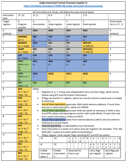
Single instruction format is more than enough!
12/11/2023 at 03:36 • 0 commentsEven simple 4 or 8-bit microprocessors or microcontrollers have many different instruction formats to encode a wide variety of instructions. How can a CPU work with just one format:
bits 15...12 11..9 8...6 5...3 2..0 register P A X Y S Execute general purpose programming language code?
Let's explain on example of a short routine which outputs to UART (MC6850 or similar) a character string terminated by zero (0x0000, all data is 16-bit, LSB 8-bit contains the ASCII code).
From uart.sif
UART_OutStr:LDA, M[X];
        IF_AZ;
        .branchto @UART_Done - $;
        MARK2;
        BRANCH;
        .into @UART_OutChr - $;
        INX, BRANCH;
        .data @UART_OutStr - $;
UART_Done:  RTS;
While this looks like regular assembly code, it is actually microcode. So it can be compiled using the "mcc" microcode compiler. This produces following VHDL code (which can be directly compiled into the system ROM):
-- L0046@00E8 0980.UART_OutStr:  LDA, M[X];
--  r_p = 0000, r_a = 100, r_x = 110, r_y = 000, r_s = 000;
232 => X"0" & O"4" & O"6" & O"0" & O"0",

-- L0047@00E9 9000.  IF_AZ;
--  r_p = 1001, r_a = 000, r_x = 000, r_y = 000, r_s = 000;
233 => X"9" & O"0" & O"0" & O"0" & O"0",

-- L0048@00EA 0006.  data16 =  @UART_Done - $;
--  data16 = 0000000000000110;
234 => X"0006",

-- L0049@00EB 6003.  r_p = STP2, r_s = M[PUSH];
--  r_p = 0110, r_a = 000, r_x = 000, r_y = 000, r_s = 011;
235 => X"6" & O"0" & O"0" & O"0" & O"3",

-- L0050@00EC 2000.  BRANCH;
--  r_p = 0010, r_a = 000, r_x = 000, r_y = 000, r_s = 000;
236 => X"2" & O"0" & O"0" & O"0" & O"0",

-- L0051@00ED FFEC.  data16 =  @UART_OutChr - $;
--  data16 = 1111111111101100;
237 => X"FFEC",

-- L0052@00EE 2080.  INX, BRANCH;
--  r_p = 0010, r_a = 000, r_x = 010, r_y = 000, r_s = 000;
238 => X"2" & O"0" & O"2" & O"0" & O"0",

-- L0053@00EF FFF9.  data16 =  @UART_OutStr - $;
--  data16 = 1111111111111001;
239 => X"FFF9",

-- L0054@00F0 4002.UART_Done:  r_p = LDP, r_s = M[POP];
--  r_p = 0100, r_a = 000, r_x = 000, r_y = 000, r_s = 010;
240 => X"4" & O"0" & O"0" & O"0" & O"2",
Each instructions engages 0 to 5 registers present in the CPU simultaneously. Register P (program counter) has 16 possible actions (4-bit in the instruction field), while registers A, X, Y, S have 8 (3-bit fields).
It is useful to look up instruction field definitions in the sifp.mcc file which is included when compiling the assembly code.
LDA, M[X];
Register X outputs content to address bus adder (code 6). Because no other register does this, the address bus value is 0 + X + 0 + 0 and it is valid (VMA = 1)
Register A loads data from the internal data bus. Because no other register outputs to this bus, it is in read mode (RnW = 1) and because there is valid address (VMA = 1), it means there will be memory read cycle. Loading A affects the AZ flag (1 if value is 0x0000).
All other registers are NOP, unaffected.
IF_AZ;
During EXECUTE phase, P (program counter) points to next address after the current instruction. P projects to internal address bus, so value is P + 0 + 0 + 0, and VMA = 1. No register is outputing value, so cycle is read (RnW = 1). Based on the value of flag (in this case A[ccumulator]Z[ero]), P is either incremented (no branch) or added with value read from memory (relative branch).
All other registers are unaffected (NOP)
.data16 = @UART_Done - $;
While all instructions are single word, P register in some cases (such as conditional) increments the value, which allows next word to be data. It this case the relative offset is branch target - current location. Value here is 0x0006, as 6 words forward is the UART_Done label.
r_p = STP2, r_s = M[PUSH];
MARK2 alias resolves to this sequence. SIFP16 can execute only 1 memory access per instruction, so it can't do both a push of return adress and load of the P (program counter). This instruction first pushes the right return address to stack:P(rogram counter): value + 2 will be output to internal data bus. This means that RnW = 0 (write to memory signal will be asserted)
S(tack): S will project value S - 1 to internal address bus, which will have value of 0 + 0 + 0 + (S - 1), VMA = 1, so result will be pushing "ahead" value of P to stack, and S will be decremented.
BRANCH;
In second part of subroutine call, a relative jump to new location must be executed. BRANCH is effectively same as IF_TRUE.
.data16 = @UART_OutChr - $;
Same relative jump target calculation like above. Note that this call is done using relative target, which allows relocatable code if the target is in the same code block (absolute jumps are also supported, a fancy compiler could differentiate and abstract the difference to produce relocatable modules).INX, BRANCH;
SIPF CPU can execute up to 5 operations in one instruction, but most often it is 1 or 2 (the code I am running now achieves 1.25 operations per instruction, or 0.625 per clock cycle, or 15.6MOPS at 25MHz clock). Here is the case when 2 independent operations are done simultaneously ("super scalar" :-))X: increments, updates XZ and XC flags - note that this operation does not project address or data, so no VMA, and RnW remains default 1.
P: projects address so address bus is P + 0 + 0 + 0, VMA = 1, there is memory read cycle (points to relative offset word below), which is added to P.
.data16 = @UART_OutStr - $;
Calculated offset is here 0xFFF9 which means 7 steps "back" which is the label UART_OutStr.r_p = LDP, r_s = M[POP];
RTS alias resolves to these two operations:P: program counter is loaded with that appears on internal data bus, which is read mode (RnW = 1) because no other register projects value ("write")
S: Stack pointer projects to internal address bus which is 0 + 0 + 0 + S, VMA = 1, this results in read ("pop") memory cycle. At the end of clock cycle, S is incremented (classic stack grows towards smaller memory address)
Very simple combinatorial logic resolves the following rules:
- If at least one register is projecting its value to internal address bus, there will be valid memory access (VMA = 1)
- If more than one register projects address, they will be added (so it is possible to do base addressing M[Y + X] for example)
- If at least 1 register is projecting its value to internal data bus, AND there is VMA = 1, there will be memory write cycle (RnW = 0)
- If more than 1 register is projecting its value to internal data bus, they will be OR'd together (there is exception if A, X, Y, S are projecting simultaneously)
With the rules above, it is also possible to have effective internal data transfer, for example:
INY, LDX, A;
Increments Y while loading X with contents of A - there is no memory operation in this case.
-
CPU control: don't decode, just execute
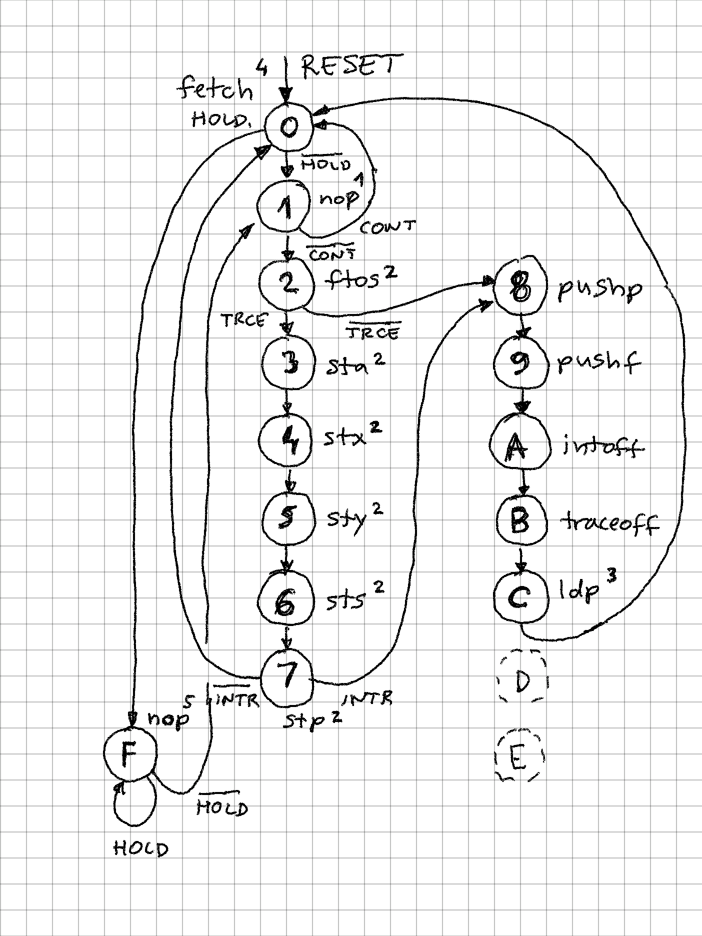
12/10/2023 at 23:33 • 0 commentsClassic CPUs execute instructions by going through a predetermined set of machine states. With SIFP16's unique design, these machine states are at the same time proper CPU instructions. This means, that regardless of the program, SIFP-16 always only executes 14 CPU instructions and goes over 14 possible states.
In absence of special execution conditions (HOLD, TRACE, INTERRUPT), only 2 instructions / states are executed:
- FETCH:
- CPU executes following instruction: r_p_M_IMM & r_a_NOA & r_x_NOX & r_y_NOY & r_s_NOS (this will generate VMA and RnW both high)
- FETCH signal is asserted on the bus (useful for debugging)
- Data bus input is loaded into 16-bit reg_i (instruction register)
- EXECUTE:
- CPU executes whatever is in reg_i
- go back to FETCH
The simplest control unit implementation could simply be a flip-flop, driving a 2->1 MUX, one input hard coded to fetch, other connected to reg_i.But to make a full-fledge processor, handling additional states makes it a bit more complex:
![]()
Notes for the diagram above:
1. Machine instruction is "NOP", but instead contents of reg_i is executed, loaded in step 0
2. If TRCE (trace condition) is asserted, all processor registers are output on the data bus, and their index on address bus. This is useful to inspect state of each register after each instruction
3. LDP loads P (program counter) from data bus, but instead of VMA (valid memory address), INTA (interrupt acknowledge) signal is asserted to indicate that an interrupt vector should be presented to the data bus.
4. FETCH cycle is started after RESET, and all other states eventually lead here
5. State / instruction 15 is a "dead loop" as long as external circuit holds HOLD high. During that time HOLDA output is high and bus is tri-state ("Z" in VHDL)
Following control signals determine the flow:
- HOLD - serviced after each fetch, before execution starts
- CONT - no interrupts or tracing, allows for fast fetch -> execute -> fetch ... sequence
- INTR - interrupt enable flag is true, and external interrupt signal went from low to high (edge triggered)
- TRCE - trace mode - external trace pin, or internal flag is set, causing all registers to be output after each instruction
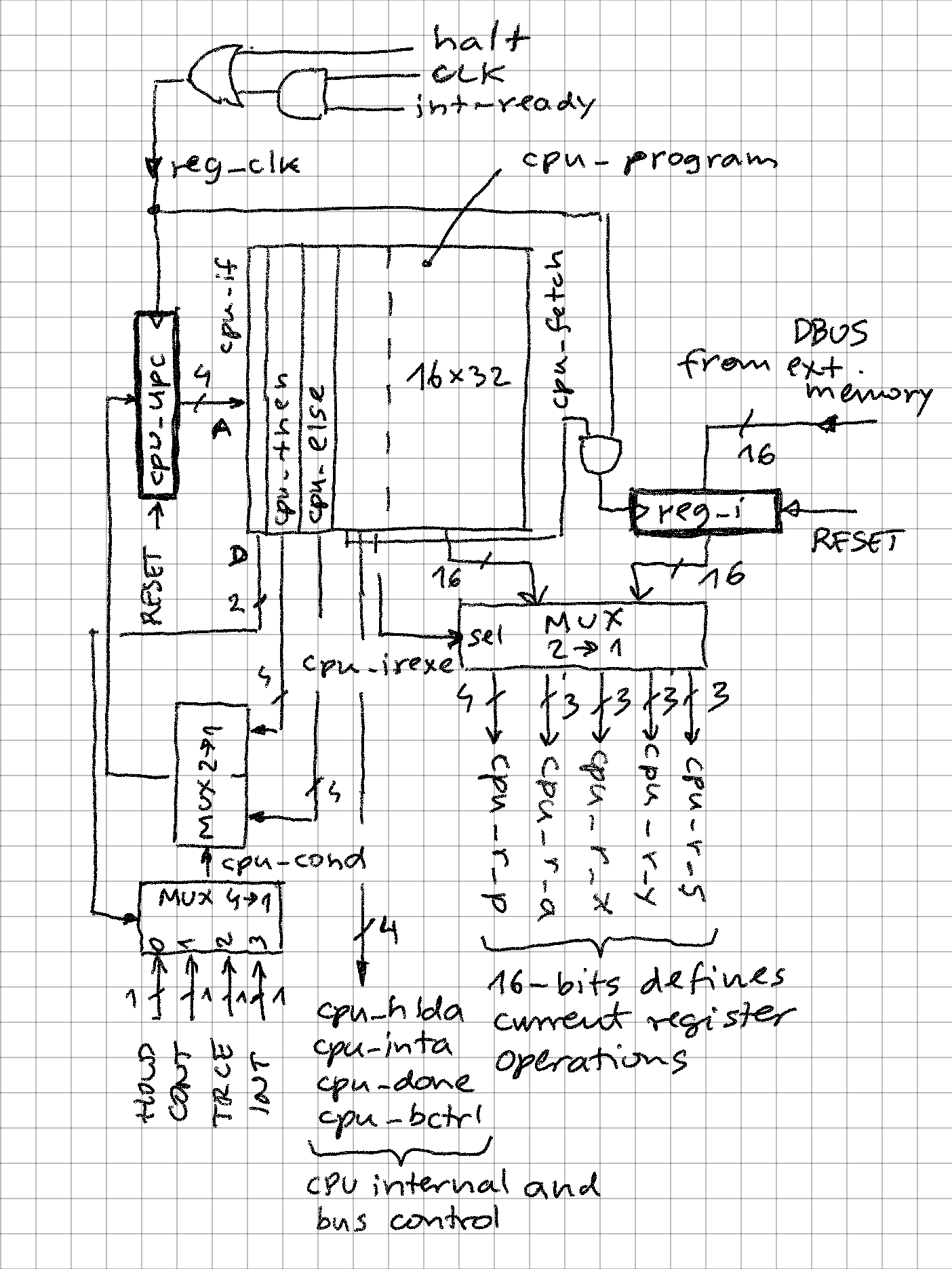
[0003]CLC:  r_a = STA, r_s = M[PUSH];
MW,FFFD DEAD
RV,  F= 0010
RV,  A= DEAD
RV,  X= BEEF
RV,  Y= BEEF
RV,  S= FFFD
RV,  P= 0073
[0004]  r_p = M[IMM], r_a = LDA;
MR,0074 0000
RV,  F= 0018
RV,  A= 0000
RV,  X= BEEF
RV,  Y= BEEF
RV,  S= FFFD
RV,  P= 0075
[0006]ACSet:  SLC;
RV,  F= 0018
RV,  A= 0000
RV,  X= BEEF
RV,  Y= BEEF
RV,  S= FFFD
RV,  P= 0076
[0007]  r_a = LDA, r_s = M[POP];
MR,FFFD DEAD
RV,  F= 0000
RV,  A= DEAD
RV,  X= BEEF
RV,  Y= BEEF
RV,  S= FFFE
RV,  P= 0077
The actual implementation of control unit is centered around a ROM of 16 instructions (2 are not used). The instruction width is 32 bits:
- 2 bits to select the internal condition ("if") - note that 5 conditions are possible, if "then" and "else" are same, this becomes "true"
- 4 bits to determine next instruction if condition is true ("then")
- 4 bits to determine next instruction if condition is false ("else")
- 6 control bits
- 16-bit instruction driving the P, A, X, Y, S registers
-- instruction word signal cpu_instruction: std_logic_vector(31 downto 0); alias cpu_if: std_logic_vector(1 downto 0) is cpu_instruction(31 downto 30); -- select condition ("IF") alias cpu_then: std_logic_vector(3 downto 0) is cpu_instruction(29 downto 26); -- next state if condition true ("THEN") alias cpu_else: std_logic_vector(3 downto 0) is cpu_instruction(25 downto 22); -- next state if condition false ("ELSE") alias cpu_hlda: std_logic is cpu_instruction(21); -- 0: bus hold (tri-state) machine cycle alias cpu_inta: std_logic is cpu_instruction(20); -- 0: load interrupt vector alias cpu_done: std_logic is cpu_instruction(19); -- 1: last machine cycle in instruction alias cpu_bctrl: std_logic is cpu_instruction(18); -- 0: alternative bus control (ABUS = register address; VMA, PnD, RnW = '0') alias cpu_irexe: std_logic is cpu_instruction(17); -- 1: execute from instruction register alias cpu_fetch: std_logic is cpu_instruction(16); -- 1: fetch -- format of lower 16-bit is exactly the same like the instructions stored in external memory! alias cpu_i: std_logic_vector(15 downto 0) is cpu_instruction(15 downto 0);![]()
Note:
- There is no "random decode logic" - output of MUX cpu_r_? drives directly 5 programmable registers in the CPU
- CPU instructions are reused to drive CPU control logic (for example LDP allows loading program counter from stack, but is here also reused to load interrupt vector etc.)
- Maximum delay path is very short, just a ROM lookup + 2 gate delays (on my old FPGA board with 50MHz max clock, CPU works are 25MHz, executing at 12.5MIPS)
- cpu_done signal allows measuring throughput (instructions per second) and also help external trace circuit to implement single stepping
- cpu_bctrl signal allows alternative driving of the bus. When low, VMA is low so in TRCE mode register output is not interpreted as memory write.
- Execution times are very predictable:
- 2 clock cycles per instruction (no trace)
- 8 clock cycles when in trace mode
- 8 clock cycles to service interrupt (this includes automatic saving of P and F registers to stack)
-- CPU program -- CPU always executes only these instructions continously -- except at step 1 when the instruction executed is coming from instruction register -- which was loaded from external memory -- this works because the lower 16 bits of the instructions in this program are same as -- instruction format stored in external memory constant cpu_program: mem16x32 := ( -- basic loop (fetch / execute) -- 0: fetch, then hold or execute if_hold & X"F" & X"1" & "000101" & c_FETCH, -- 1: execute, then continue (fetch next instruction) or special path if_cont & X"0" & X"2" & "001110" & c_NOP, -- trace routine outputs register index on A bus and value on D bus -- 2: output F(flags), if trace then output other regs else push regs (interrupt) if_trce & X"3" & X"8" & "000000" & c_FTOS, -- 3: output A, continue if_intr & X"4" & X"4" & "000000" & r_p_NOP & r_a_A & r_x_NOX & r_y_NOY & r_s_NOS, -- 4: output X, continue if_intr & X"5" & X"5" & "000000" & r_p_NOP & r_a_NOA & r_x_X & r_y_NOY & r_s_NOS, -- 5: output Y, continue if_intr & X"6" & X"6" & "000000" & r_p_NOP & r_a_NOA & r_x_NOX & r_y_Y & r_s_NOS, -- 6: output S, continue if_intr & X"7" & X"7" & "000000" & r_p_NOP & r_a_NOA & r_x_NOX & r_y_NOY & r_s_S, -- 7: output P, if interrupt then push regs else fetch (new instruction) if_intr & X"8" & X"0" & "001000" & r_p_STP & r_a_NOA & r_x_NOX & r_y_NOY & r_s_NOS, -- interrupt routine pushes P and F on the stack, disables tracing and interrupts, and then load the int vector -- 8: push P, continue if_cont & X"9" & X"9" & "000100" & c_PUSHP, -- 9: push F, continue if_cont & X"A" & X"A" & "000100" & c_PUSHF, -- A: turn trace flag off, continue if_cont & X"B" & X"B" & "000100" & c_INTOFF, -- B: turn interrupt enable off, continue if_cont & X"C" & X"C" & "000100" & c_TRACEOFF, -- C: load intrrupt vector, then fetch next instruction if_cont & X"0" & X"0" & "010100" & c_LDP, -- unused, reserved for future use -- D: unreachable nop if_cont & X"0" & X"0" & "000100" & c_NOP, -- E: unreachable nop if_cont & X"0" & X"0" & "000100" & c_NOP, -- bus hold routine -- F: hold (tri-state) until HOLD signal detected low, otherwise execute if_hold & X"F" & X"1" & "100000" & c_NOP ); - FETCH:
SIFP - Single Instruction Format Processor
A super-scalar, reduced instruction set processor where microcode and machine code are the same thing!