 Michael Schembri
Usage: kicadcontour <options> <filename>
filename :- kicad pcb output file.kicad_pcb
- -m (don't do conversion to raster but use map.png directly)
- -f process front layer of PCB (defaults to Bottom Layer processing)
- -p (change pxmm scale conversion)
Files Created
- map.png - Vector to raster conversion
- cpp_image.png - wall paper art of your PCB
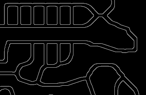
- trace.png - Edge detection image
- kic.gcode - Final Gcode
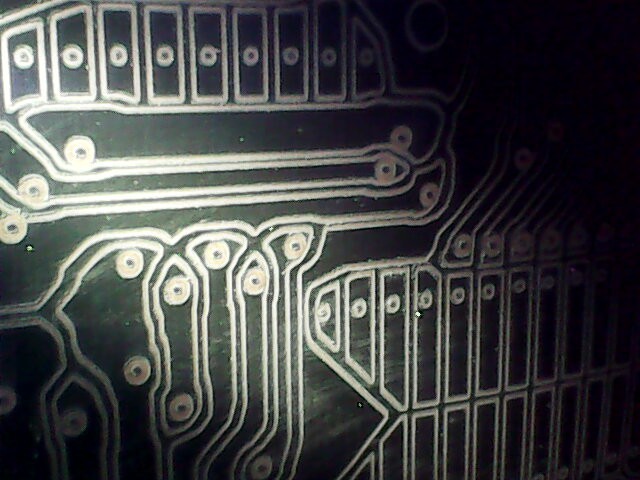
Vector to Raster conversion
Raster to conversion is done using pxmm scale (pixels per mm). The resulting image map.png is then processed to create the isolation routing paths. pxmm default is set to 30. The scale is modifiable, however smaller pxmm reduces precision of paths created, whereas larger pxmm increases time to process.
Gcode Creation
The paths are converted to gcode using a path following algorithm in OpenCV. Gcode is scaled back to original dimensions. Drill holes are appended to the gcode, using the original scale.
Errors
OpenCV contour following does not always make close contours. However, the gaps (at a pxmm of 30) are very small (in the region of 0.05-0.08mm). The tool width is larger than that, so it should not pose any problems. However, please comment on improvements.
OpenCV contour following also creates some small artefacts. However, these are not visible, but might have a minor impact on milling times.
Recommendation
I always optimize gcode before milling. This reduces unwanted travel time. I usually use https://xyzbots.com:4000/gcode-optimizer/


 Lutetium
 ElectroBoy
 Lithium ION
This looks great and I expect to try it soon.
I'm a little confused. One of the logs here and mostly the repo indicate that you use this with a laser cutter. ?. Are you ablating a resist layer for etching? Does that save you a lot of laser time?