Close
0%
0%

USB-C PCB Socket

An investigation into how effective is a USB-C socket made using PCB traces.

Similar projects worth following
I want to look into how feasible it is to create a USB-C socket directly on PCB material. This would mean there would no need for a connector, which in some cases can be quite expensive.

Please Note: Before I get any further into this; this is a research project. I would love to have a finished product at the end of this, but I am aware from the start that this is not likely to work. 

What am I doing?

In this project I want to answer once and for all. "Is it possible to create a USB-C socket with PCB material to remove the need to use a USB-C socket (which can be quite expensive in some cases)? 

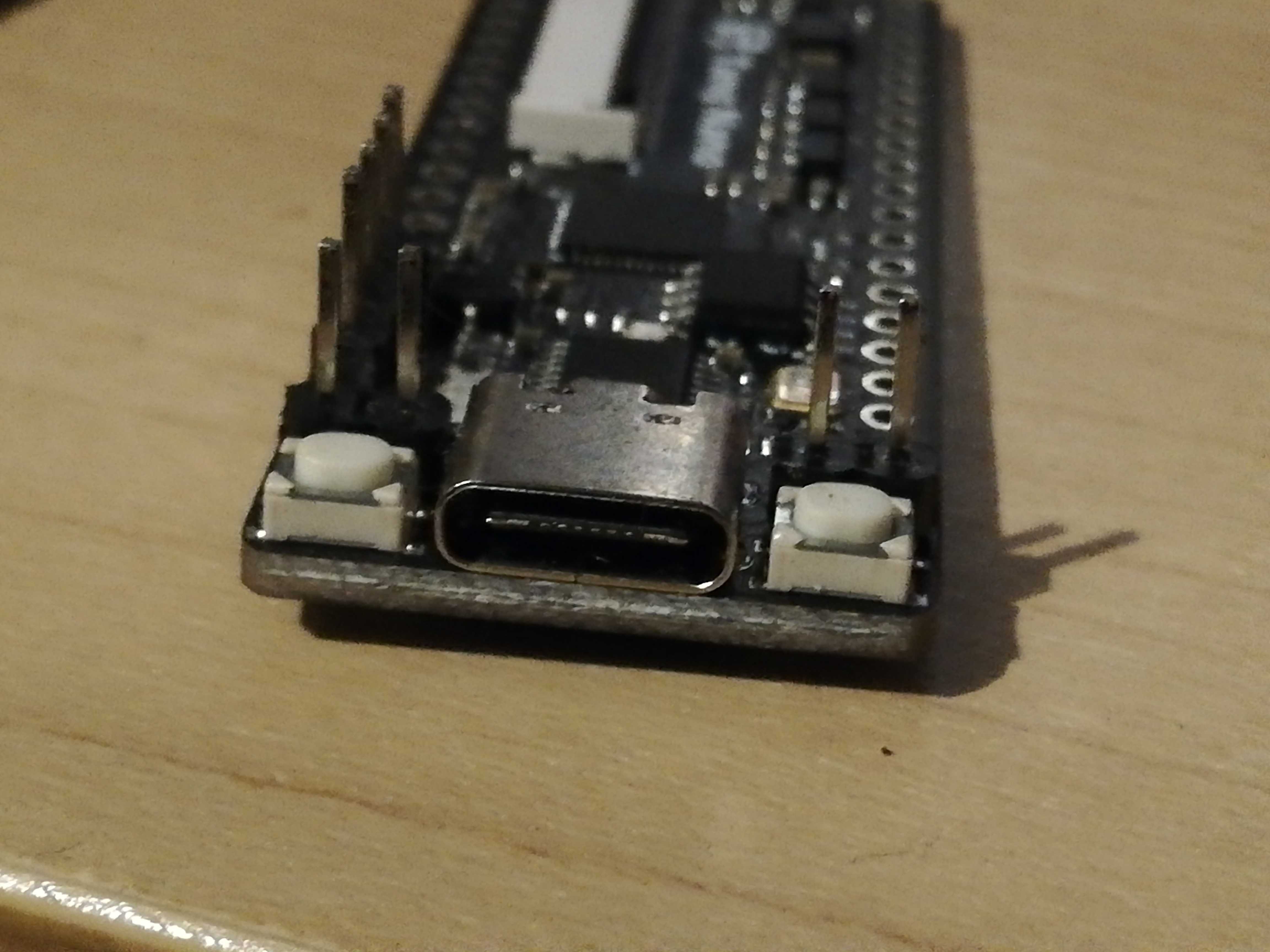
USB-C sockets use a thin tongue to connect with up to 24 contacts inside the USB-C plug, i'm hoping this can be recreated using a PCB. 

Why am I doing this?

When I first thought of using this method the first thing I did was go to google and ask if anyone had ever tried this before. I have seen plenty of examples of using PCB pads as a  USB-A plug and even an example of a Micro-USB socket mimicked on a PCB. But there was no obvious examples of this before. 

I was intrigued that there was so little information available especially as USB-C is starting to become a staple of the engineering and maker communities.

Has this been done before?

After talking about my first initial PCB prototypes on twitter, it was brought to my attention this in fact, had been tried by a few engineers and designers on some of their own boards.

This is a design by Jan Henrik Hemsing. He states that he had connection issues and had to use an outer casing

The EFM8UB1 Breakout seems to be able to use it quite effectively which can be found here

There was also attempts by Bobricus

And also by Deshipu

But unfortunately not much success in those cases.

Disclosure: I'm sorry if there are others, the above are the only ones brought to my attention.

SO, (once again) Why am I doing this?

I feel most of the people who have tried this method have been taking the approach of adding it to a product design. Which is creative and astounding work and I am very grateful for the insight it provides. Adding it to a product can be difficult because if it doesn't return a satisfactory result then the whole thing is normally dropped for a more tried and tested method. Honestly, I would do exactly the same in those cases. But I would like to take a deep dive into the question of is this method possible, given material cost and manufacturing constraints.

What am i trying to achieve?

What I want to achieve from this is:

  • answer the question of 'Can this work?'
  • Find what the constraints are.
  • Fully document what happens at each stage of this investigation.
  • Provide all my working files during and at the end of this process.
  • If this doesn't work, explain in detail why it doesn't work.


Wish me luck :) I hope I can do this Justice.

  • PCB arrival

    Gee Bartlett01/25/2021 at 09:24 0 comments

    Just a quick one not sure why I didn't do this at the time. The PCBs arrived back on 17/08/2020!!!!

    The board a small and cute.
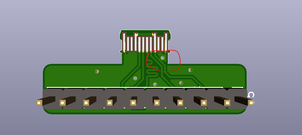
    There is, unfortunately, a small fault on these boards where VBUS is bridged to GND.

    The annular ring on the via has caused the short easily fixed with a sharp knife though and will make sure that it is fixed on the next PCB spin :)

    Next is testing the fit and connection reliability.

  • In the Beginning

    Gee Bartlett08/10/2020 at 09:39 0 comments

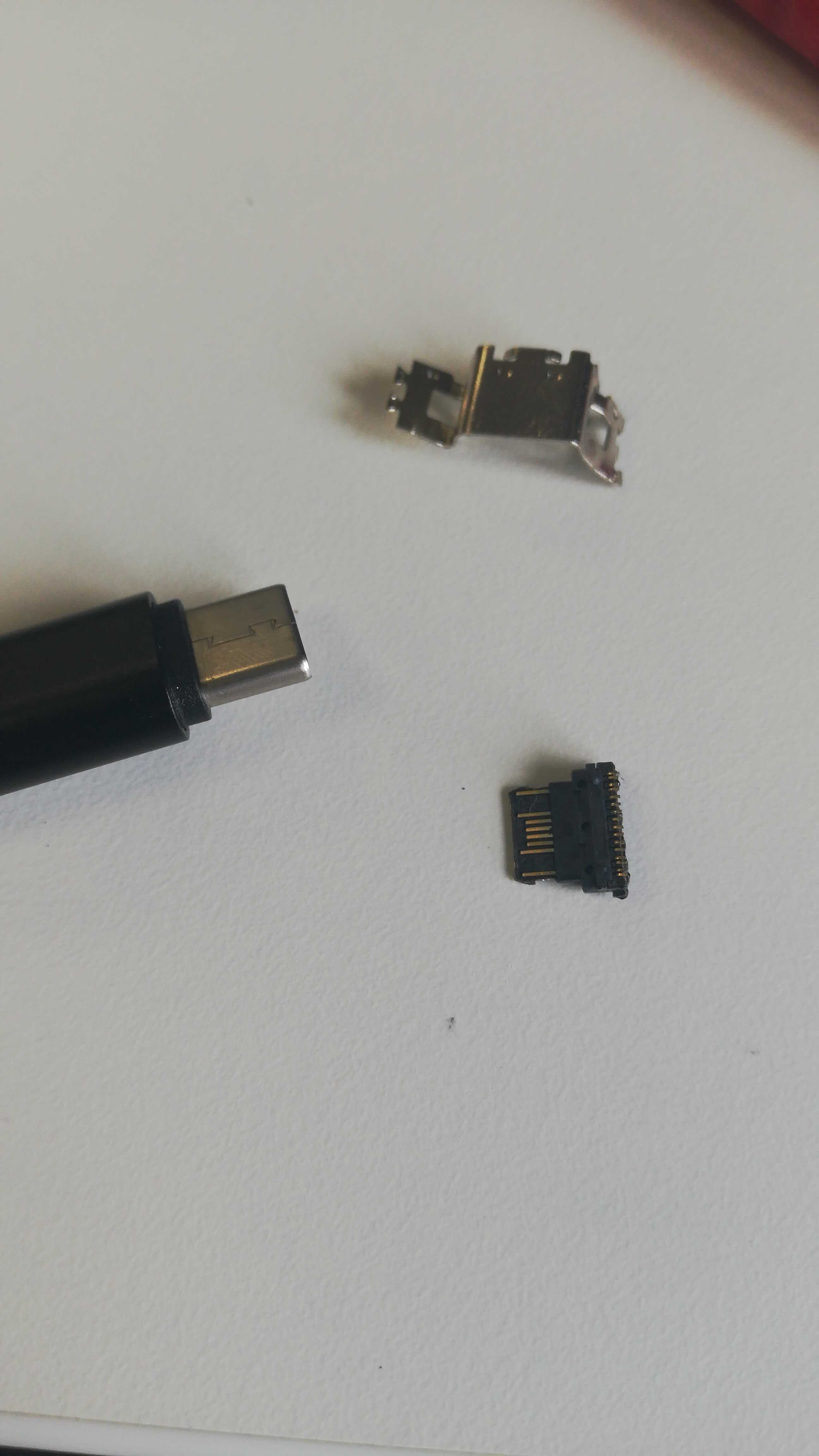
    I have been looking at this project for about a month now. So as you can imagine i have done some initial work and investigation, this involved looking into the USB 3.1 specification and tearing apart a a socket or two to see how the connections are made with the USB-C plug. 

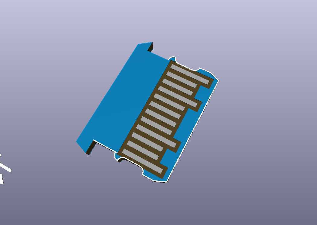
    So it was time to fire up KiCAD and get a design for the socket drawn out. (files available in the Github links provided)

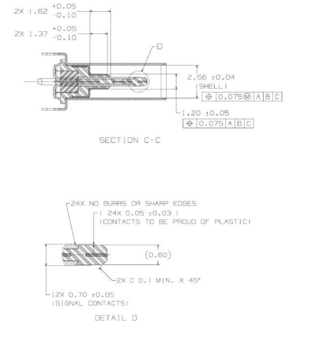
    I tried to stick to the specification as much as possible the difficulty is the the sockets 'tongue' should thicken out once it is past the contacts. see below.

    Some who have tried this have reported intermittent contact this could be the reason. In the end I decided to push ahead with a design 0.6mm PCB material. 

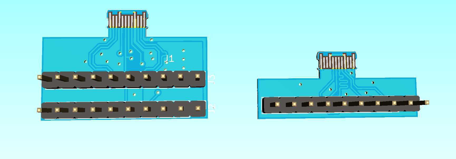
    I routed out two designs in the end, The Left-hand design has every contact broken-out from the connector including the differential USB-SS traces all length matched as best as I can. But for the moment I'm going to focus on the right-hand design which breaks out the USB 2.1 traces (length matched to hopefully allow USB-HS communication) VBUS, CC1, CC2, SBUS1, SBUS2 and GND. I want to experiment a little with the Side-Bus as the spec allows low speed transfer might think about trying the 1-wire protocol. 

View all 2 project logs

Enjoy this project?

Share

Discussions

SantWorth⌛ wrote 04/04/2023 at 22:40 point

that's so neat, looking for more

  Are you sure? yes | no

ExplodingWaffle wrote 01/11/2021 at 11:10 point

hey, did you ever get around to ordering these? wanted to try something similar and these are the only kicad footprints i could find.

  Are you sure? yes | no

Gee Bartlett wrote 08/09/2020 at 22:16 point

Thanks for the encouragement. I'm hoping so at least it should answer some unanswered questions.

  Are you sure? yes | no

Ken Yap wrote 08/08/2020 at 23:50 point

Kudos on giving a go. At the very least you will generate useful information. Maybe you will even crack it. 👍🤞

  Are you sure? yes | no

Similar Projects

Does this project spark your interest?

Become a member to follow this project and never miss any updates