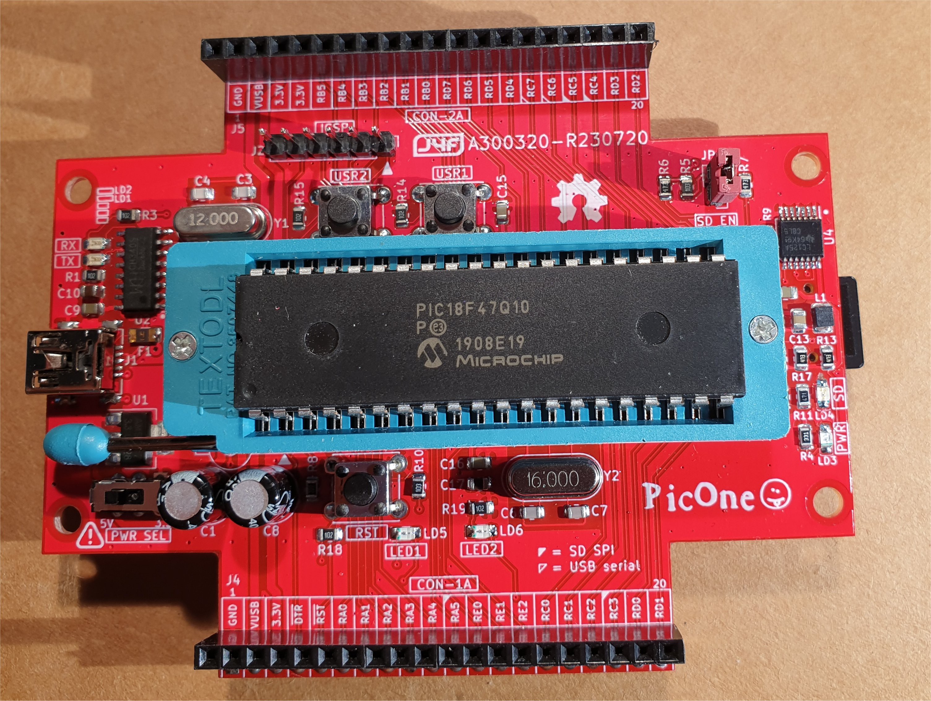
I was searching a DIL MCU for another "project" and found this one that seems interesting. It is cheap and with a lot of features, so i did a board to play with it.
PIC18F47Q10 main features:
- internal 64MHz oscillator
- 128 KB Flash Program Memory with self read/write capability
- 3728 Bytes Data SRAM Memory
- 1024 Bytes of EEPROM
- 10-bit ADC, 35 channels
- 8 x Configurable Logic Cell (CLC)
- 2 x I2C/SPI
- 2 x EUSART
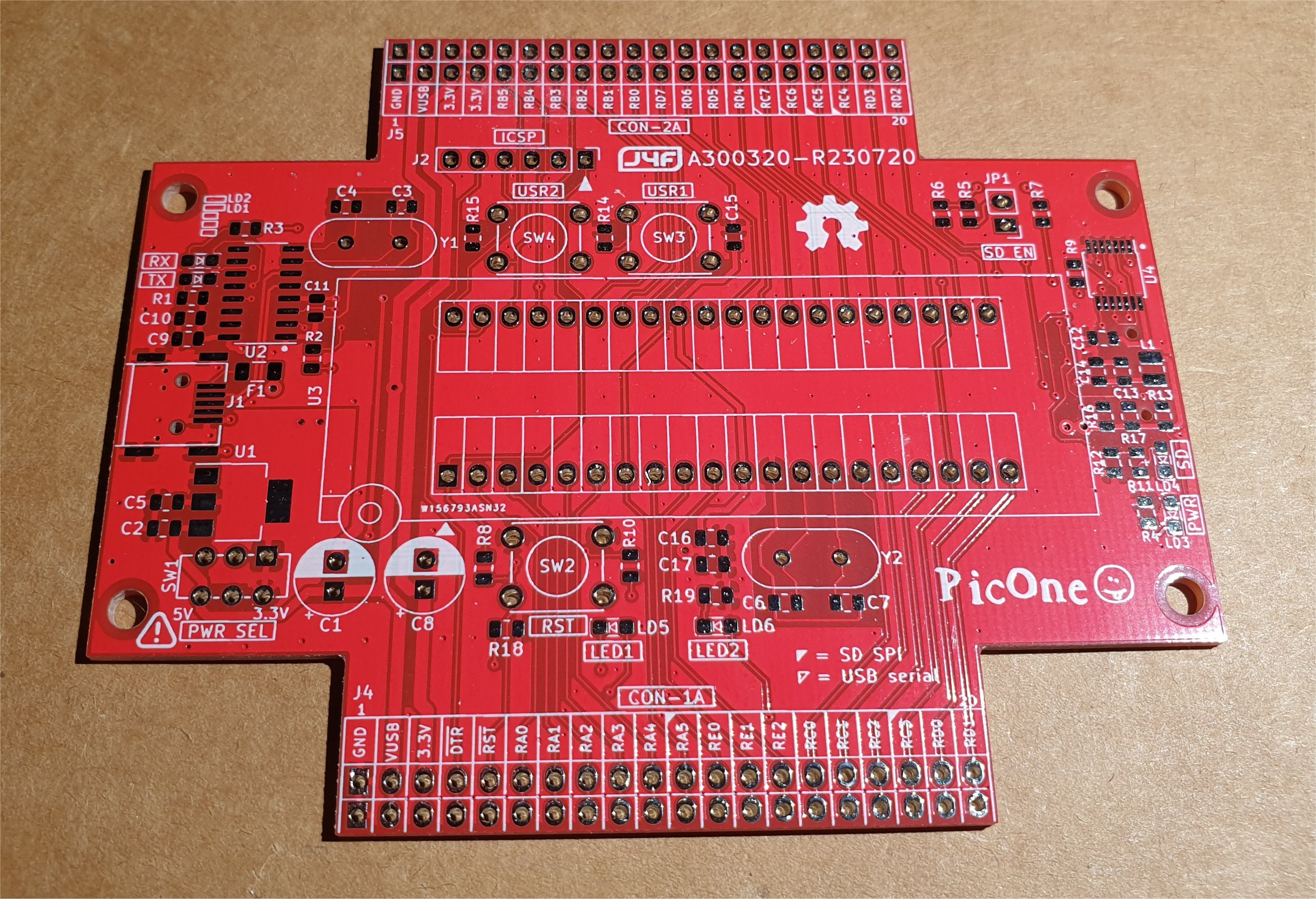
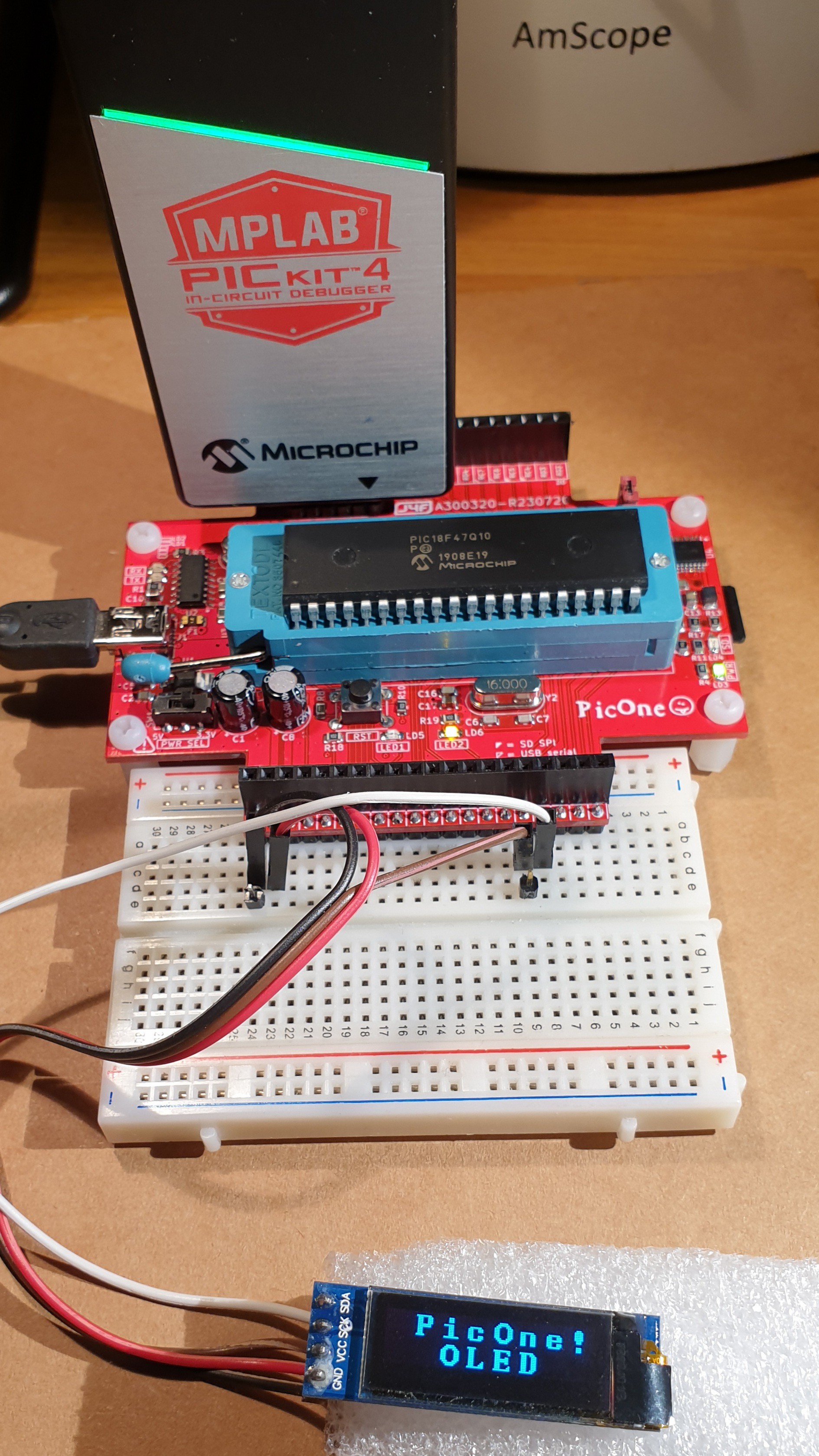
PicOne main features:
- onboard USB-serial adapter
- onboard micro-SD with level translators
- power selector (5V or 3.3V)
- ICSP standard connector
- 2 user keys
- 2 user leds
- ZIF or standard MCU socket
- plug-able into breadboards

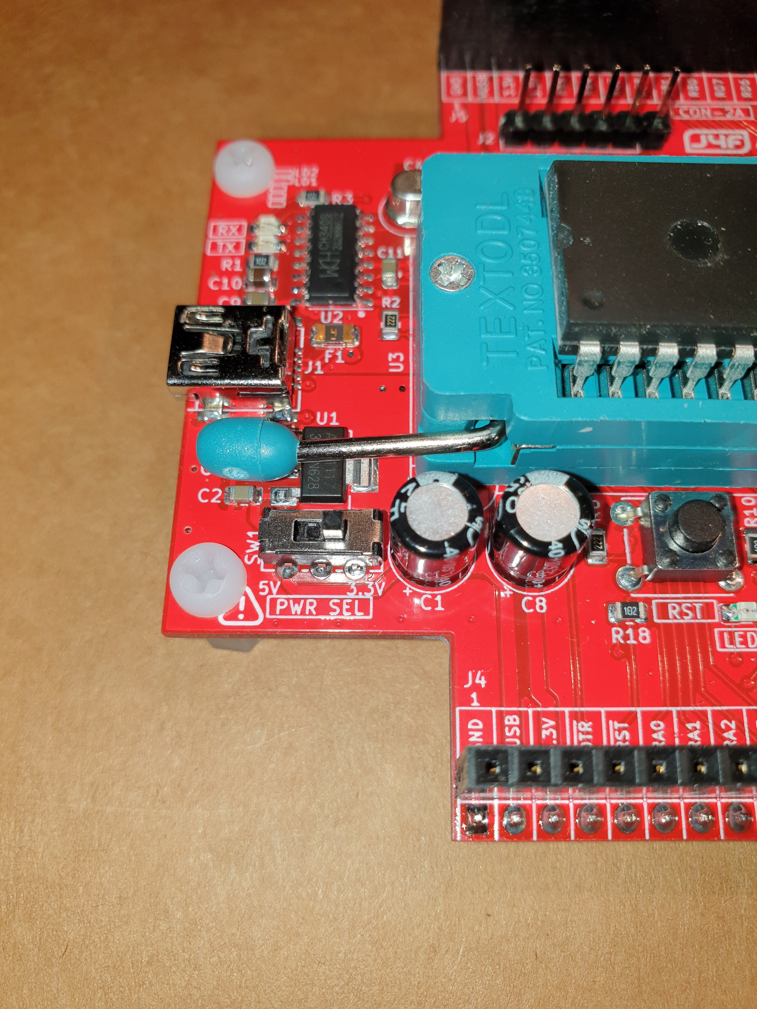
SW1 (PWR-SEL)
The SW1 switch allows to select the working voltage for the PIC MCU (U3) and for the USB-serial adapter (U2). It is possible select 5V or 3.3V. This will change the corresponding logic levels of the I/O pins.
Please note that the level translator U4 takes care to allow the use of the micro-SD regardless the position of the power selector SW1.
WARNING: the SW1 switch position must be changed only when the board is not powered!
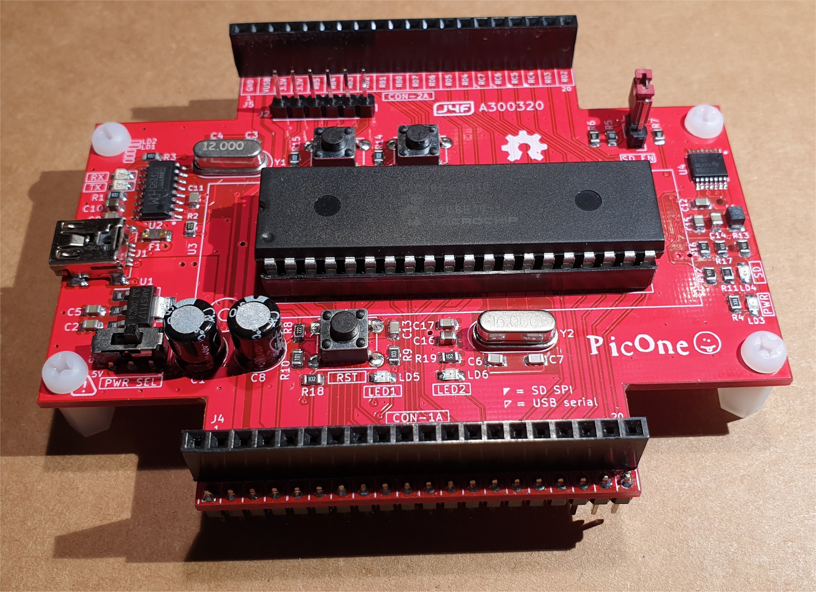
C6 AND C7 CAPACITORS
If you use a ZIF socket for the MCU, C6 and C7 (see the schematic) must be 22pF (NPO, 50V rated). If you use a normal socket C6 and C7 must be 27pF (NPO, 50V rated). This results from a higher pin to pin capacity of the ZIF socket than the normal one.
In the following image a board with a normal socket (previous PCB revision):
SJ1 AND SJ2 SOLDER BRIDGES
To allow the LED1 and LED2 led to turn on you have to bridge the two solder jumpers SJ1 and SJ2 on the bottom side of the PCB.
JP1 (SD-EN) JUMPER
To enable the onboard micro SD you have to jumper JP1 (SD-EN).
If you want use the RA4, RC5, RC3, RC4 MCU pins as general GPIO (they are used as CS, MOSI, SCK and MISO signals for the onboard micro-SD), leave JP1 open. This will disable the U4 level translator used for the micro-SD (see schematic).
If you are using the RC4 MCU pin as general GPIO (JP1 open), take into account that when the MCU is powered at 5V there might be a small current (about 3mA @ 5V) trough R9 if the RC4 pin is driven HIGH. So an external logic must be able to provide it eventually.
THE ICSP (J2) CONNECTOR
To program/debug the PIC MCU you need a PicKit or another suited programmer. The ICSP (J2) connector allows to connect the programmer to the board. On the PCB there is a mark for the pin 1 that must mach with the corresponding mark on the programmer. In the following image is shown the a PicKit4 directly attached on the ICSP connector:
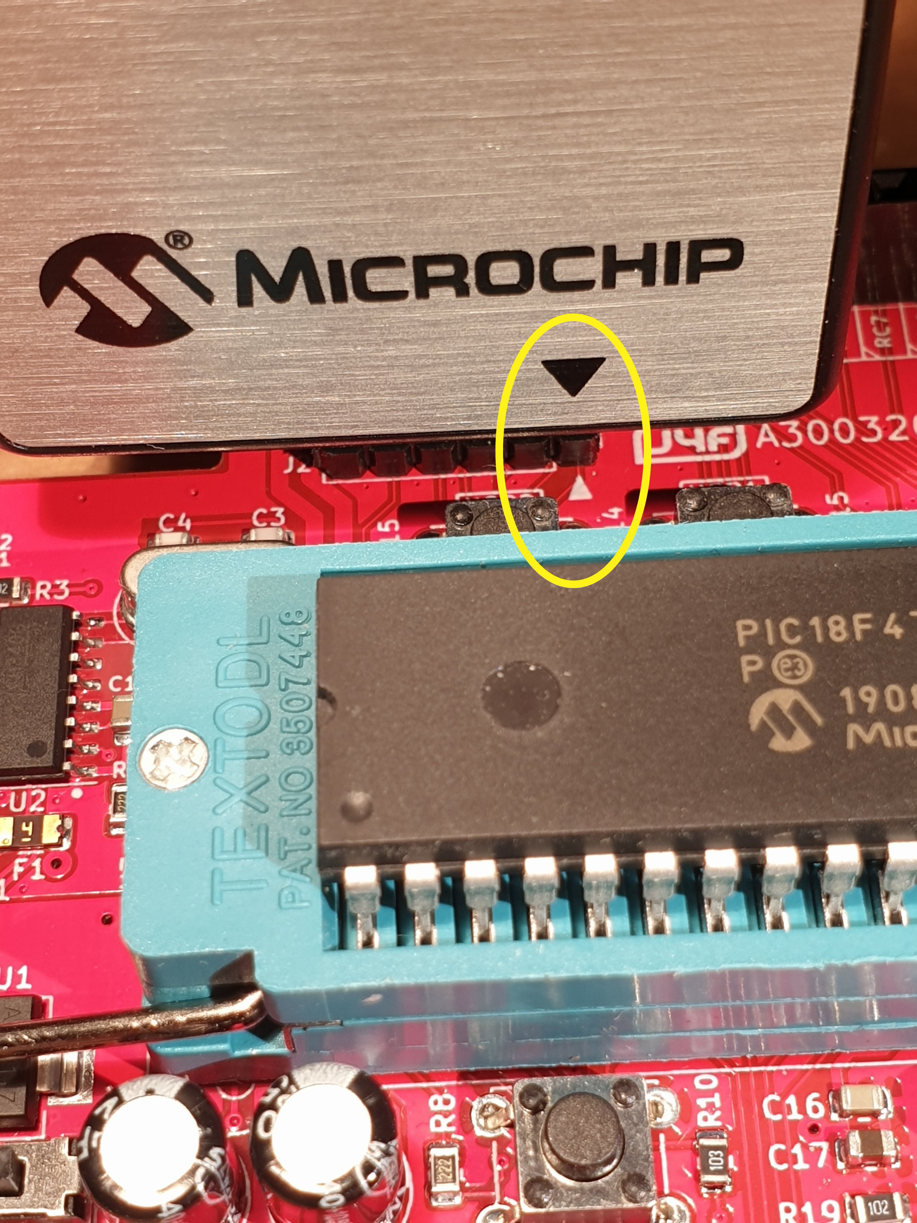
WARNING: Remember to power off the board before to connect or remove the PicKit programmer! (see the PicKit Manual for further information).
WARNING: The programmer must be set to "power the target from the board".
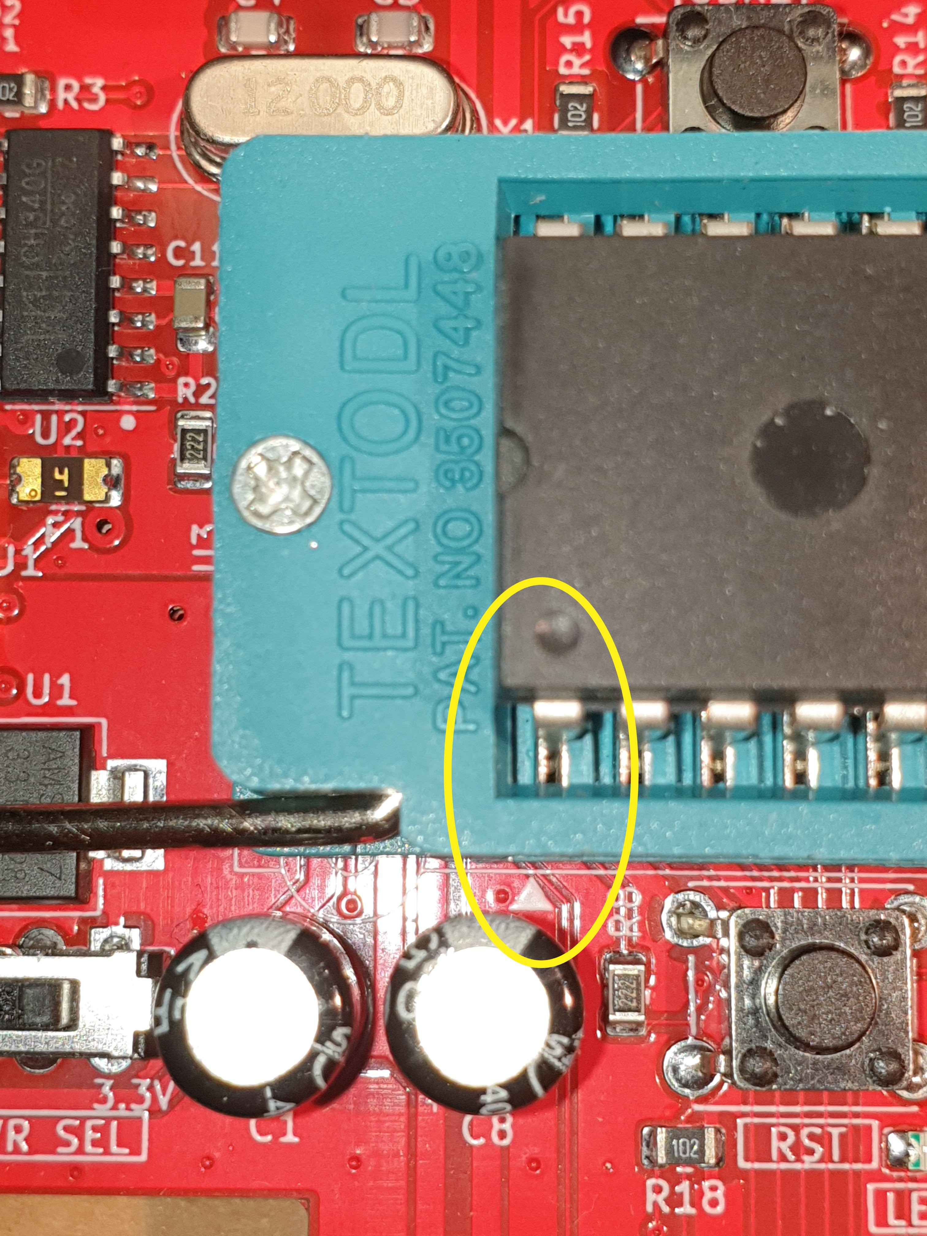
INSERTING THE MCU (U3) INTO THE ZIF SOCKET
When inserting the PIC MCU (U3) into the ZIF socket pay attention to the pin 1 mark on the PCB:
SOFTWARE EXAMPLES
In the Files section there is a zip files with some SW examples made with MPLABX v5.40 and using the MCC code configurator.
WHERE TO GET A PCB
I've prepared an "easy" link to get a small lot (5 pcs minimum) of PCB. The link is this one.
 Just4Fun

 Keith
Keith
 Charles Lakins
Is a PICKIT 3 suitable for programming a PIC18F47?
Regards,
Jan