Close
0%
0%

System K8

The massively versatile All-in-One computing system

Public Chat
Similar projects worth following
After my latest Z20X computer (as seen in http://z20x.computer), I decided to make something different altogether. A universal soft-core platform capable of emulating a large variety of systems. Yet, unlike all other FPGA-based boards, this one is actually thought for manual assembly by an average hobbyist and without requirements for special equipment. All parts except two are through-hole but the footprints are hybrid to also enable use of SMT (1206 size) components in case the user wants it that way.The K8 project was born - probably the first and only FPGA board that a user can assemble entirely from scratch

The board has a number of connectors (power supply either from a 2.1mm core barrel connector, or USB), HDMI output for video, 3.5mm stereo jack, three USB ports, an Ethernet port, and also a SD card. It also has three expansion header receptacles and a header for additional matrix keyboard.

In terms of processing power, K8 is built around a very interesting FPGA from GOWIN. It is a 144-pin TQFP package (not BGA as most of the others!!!) and includes internal non-volatile bitstream memory as well as 32Mb PSRAM in addition to the FPGA block RAM. So that makes is a pretty well integrated package, ideal for the purpose. The on-board FPGA can be upgraded by installing an additional module in the emulated PGA socket around it. It can also work alongside the module. There is a jumper for setting up the needed configuration model.

There is also a separate 512Mx8 NAND flash on board, to be used as external storage. The Ethernet is handled in a simple way via SPI and ENC28J60 controller. There is also a separate MCP2221A USB-to-UART bridge to enable a lightweight console in the system.

The power supply is built from a 5V high-current LDO which provides the main power supply, from which then 3.3V and 1.8V are internally derived for the rest of the electronics. In case the power comes from the USB, the input LDO is bypassed. A bi-colour LED indicates the current mode of operation.

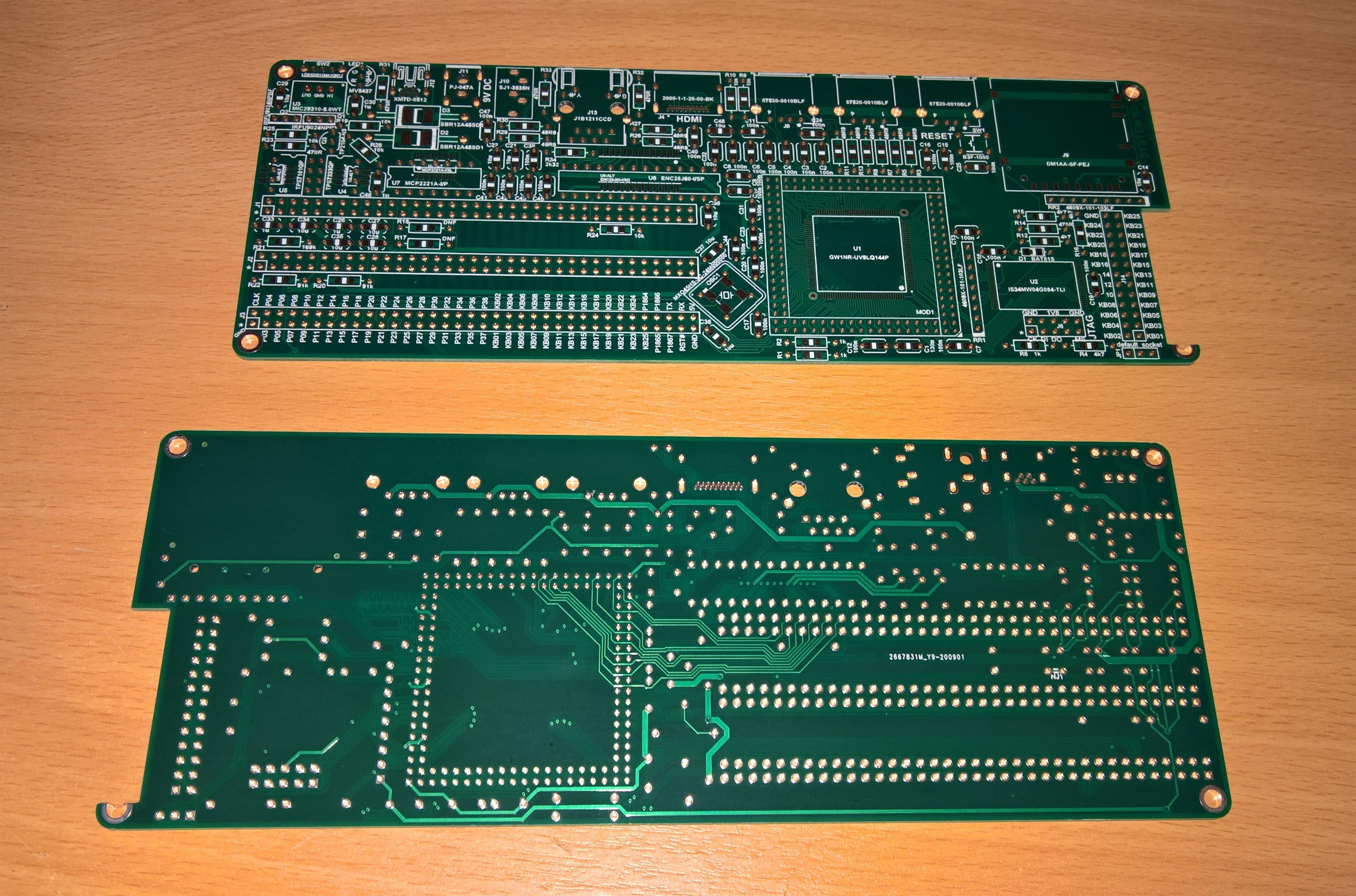
Because of the very high density of through-hole components, I was forced to do the PCB on 6 layers as there was simply not enough room for the traces otherwise. An additional complication was the need to observe the impedance and length matching for all high-speed ports, as well as an ergonomic model for the layout in order to prevent external wires crossing on top of each other, etc.

The PCB is 200 x 75 mm with a view to have it installed in a purpose-made enclosure, probably along with a separate keyboard. Alternatively an external USB keyboard can be used which leaves the keyboard header available for other needs.

The grand plan is to have a few early prototypes tested, and then hopefully offer a commercially available kit so other people can enjoy building their systems too.

PCB.step

step - 22.20 MB - 02/08/2021 at 10:55

Download

PCB.pdf

Adobe Portable Document Format - 9.07 MB - 02/08/2021 at 10:55

Preview

Assembly Drawings.pdf

Adobe Portable Document Format - 512.86 kB - 02/08/2021 at 10:55

Preview

BOM_K8_TH.xls

ms-excel - 50.50 kB - 02/08/2021 at 10:55

Download

BOM_K8_SM.xls

ms-excel - 49.50 kB - 02/08/2021 at 10:55

Download

View all 6 files

  • Finally the FPGA arrived

    Kn/vD11/07/2020 at 09:40 0 comments

    After about 2 months of waiting the FPGA finally arrived!

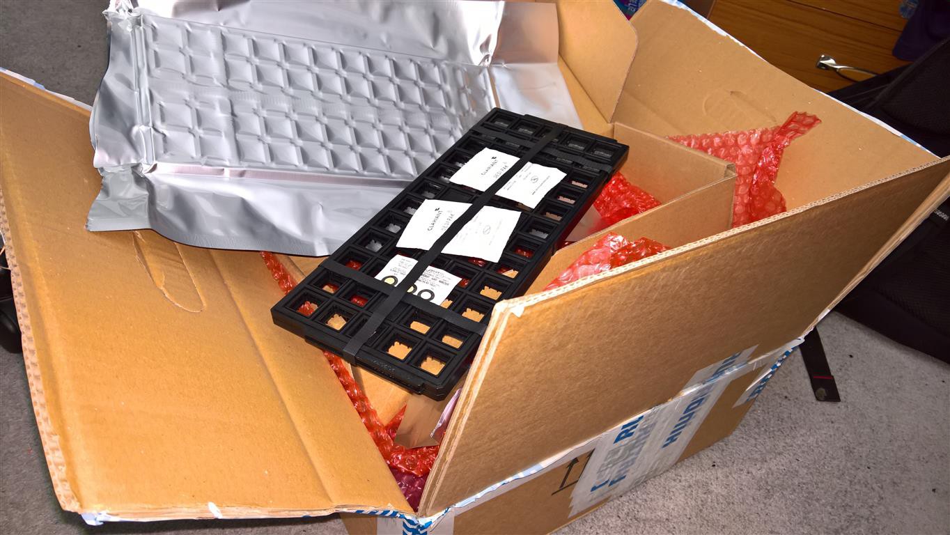
    One thing I noticed - this is surely the most ridiculous waste of packaging I've seen in my life. A box the size of a microwave oven filled with bubble wrap holding another box filled with bubble wrap holding a vacuumed foil holding a plastic tray. 

    All that for 10x TQFP ICs samples :)


    Grinning face

  • Schematic!

    Kn/vD10/14/2020 at 11:43 0 comments

    Purchasing samples from Gowin turned out a long journey. Initially they were supposed to be here by Oct 10, chasing them now and their current status is still unknown. All other parts in the system have been sitting in a box and waiting for that most important one to be put on the board first.

    Anyway, I just published the early version of the schematic in the open. Keeping fingers crossed there won't be any mistakes there. 

    As always, feedback and suggestions are welcome!

  • Boards!

    Kn/vD09/09/2020 at 11:25 3 comments

    Arrived today and look beautiful. Now expecting parts.

  • Just ordered the first PCBs

    Kn/vD08/31/2020 at 15:51 0 comments

    JLC. A six-layer PCB is pretty expensive with its one-off setup costs, but hopefully it will be worth it. I have assembled two separate BOMs - one "default" with through-hole components, and a second with SMT parts. All links but one are from Digikey; the FPGA itself is unfortunately not available there, but Mouser have it, so there you go...

View all 4 project logs

Enjoy this project?

Share

Discussions

Similar Projects

Does this project spark your interest?

Become a member to follow this project and never miss any updates