Beast Devices
-
Assembled the board
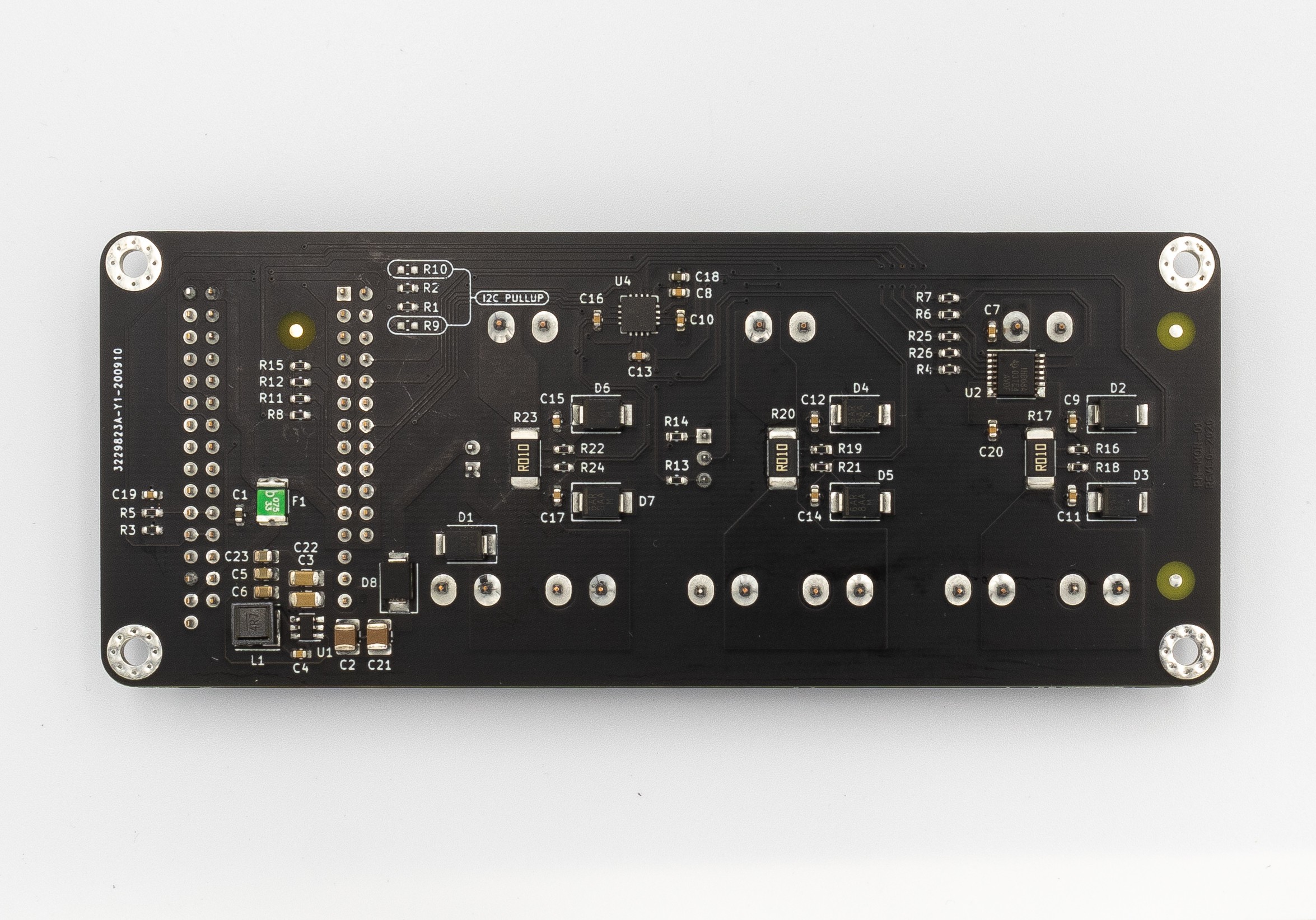
11/05/2020 at 19:21 • 0 commentsI have assembled the first board and have done some test. Everything works fine, except that I have swapped the I2C lanes, but it is easy to fix for the next PCB spin. :)
![]()
![]()
-
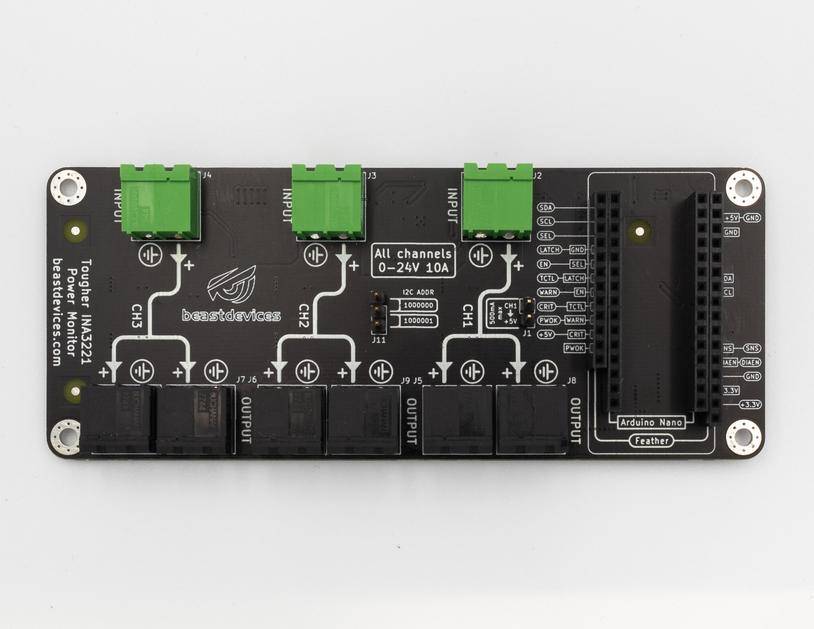
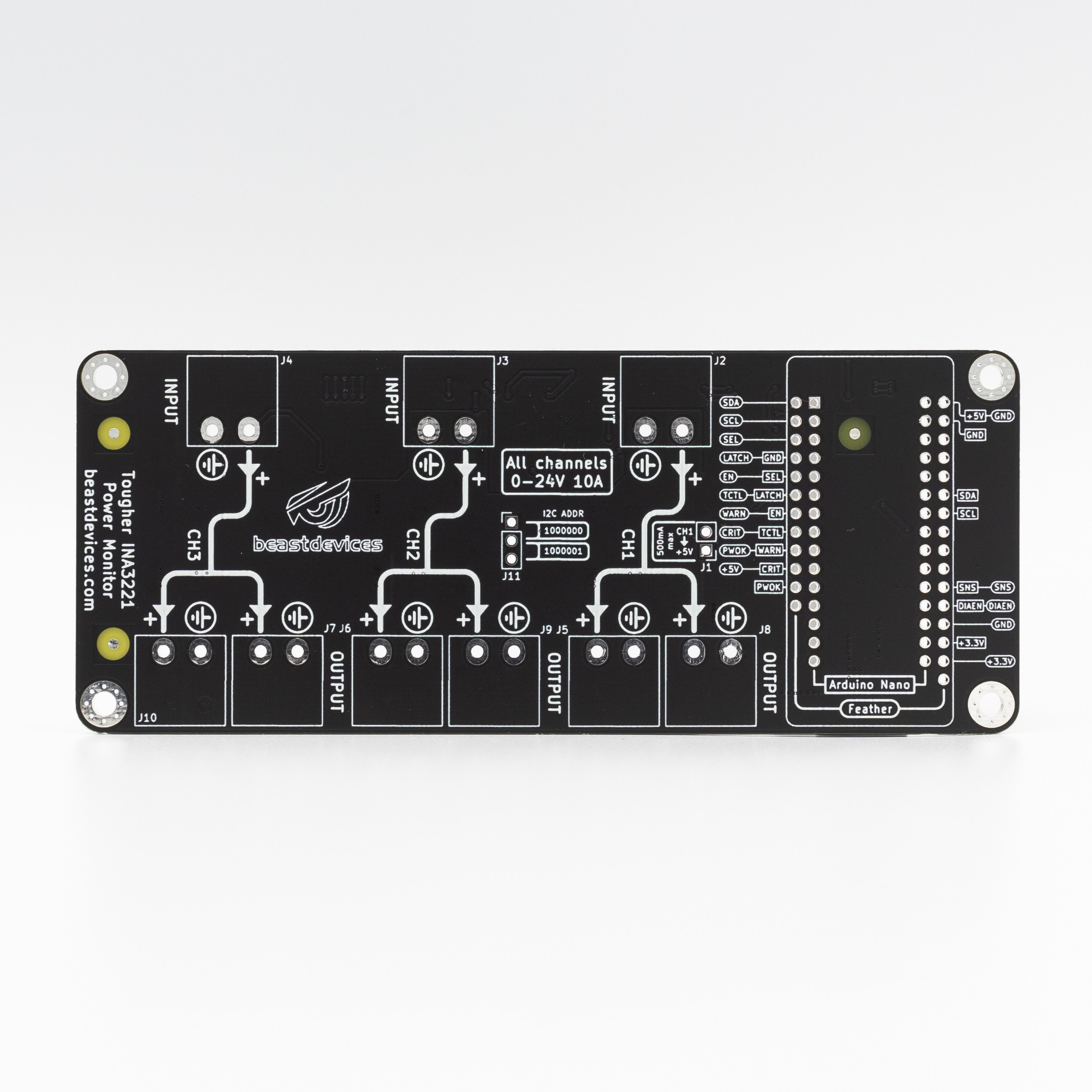
PCBs received
09/22/2020 at 08:27 • 0 commentsGot the PCBs, of course with the matte black solder mask.
![]()
![]()
![]()
-
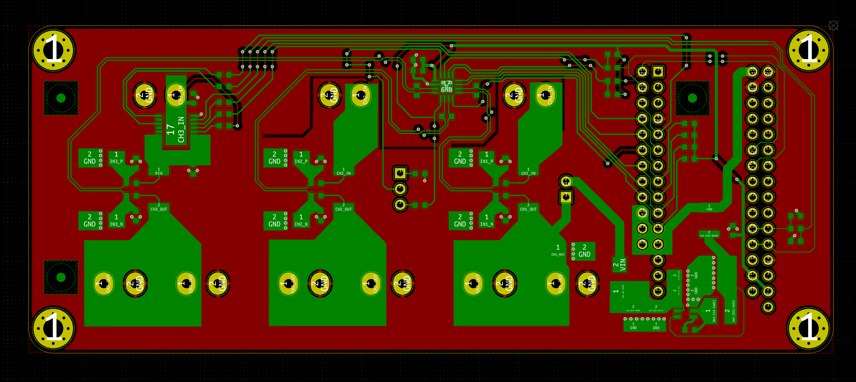
Designing the PCB
09/10/2020 at 07:48 • 0 commentsI wanted to keep the design 2-layer, and with some insignificant shortcuts, I kept it at two layers. I have tried to avoid large currents to pass around INA3221 to prevent ground bouncing, so I added some cutouts in the ground. Cutouts are made so that differential traces from current resistor don’t experience ground plane breaks. I didn’t add any ground pours on the bottom layer, because it wouldn’t add any significant benefit that I can see. It would just introduce more headache with controlling where the ground current are going. The ground path in the power area is solid and uninterrupted, and the ground path in signal areas is good enough.
The size of PCB is 130 mm by 53 mm, and could probably be made a bit smaller with a 4-layer design, by having Feather/Arduino sitting on top of everything. But this approach would also make it harder to do any changes later on. In the current design, if I want to change from Feather/Arduino to something else, I don’t have to modify anything in the power area.
![]()
![]()
-
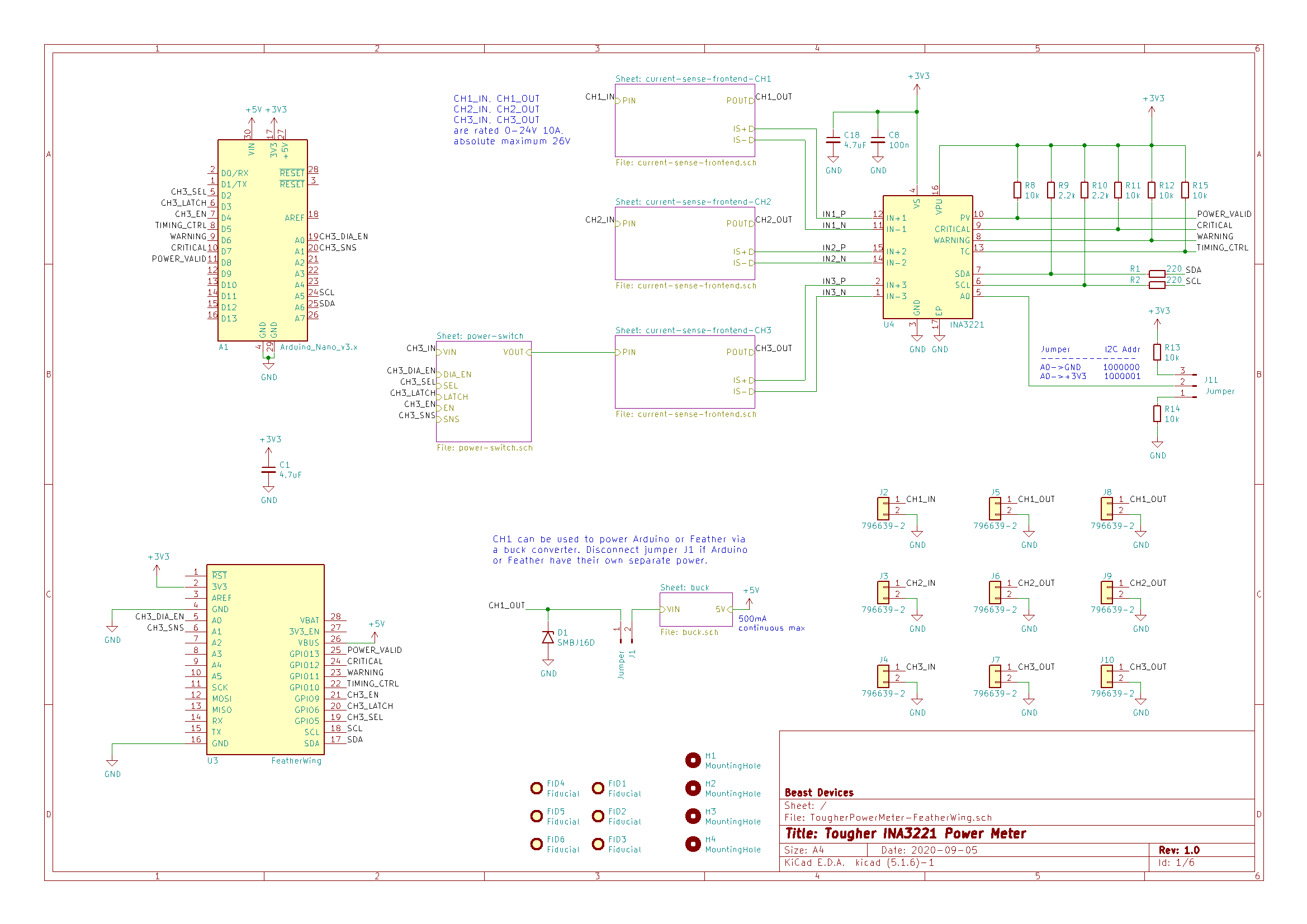
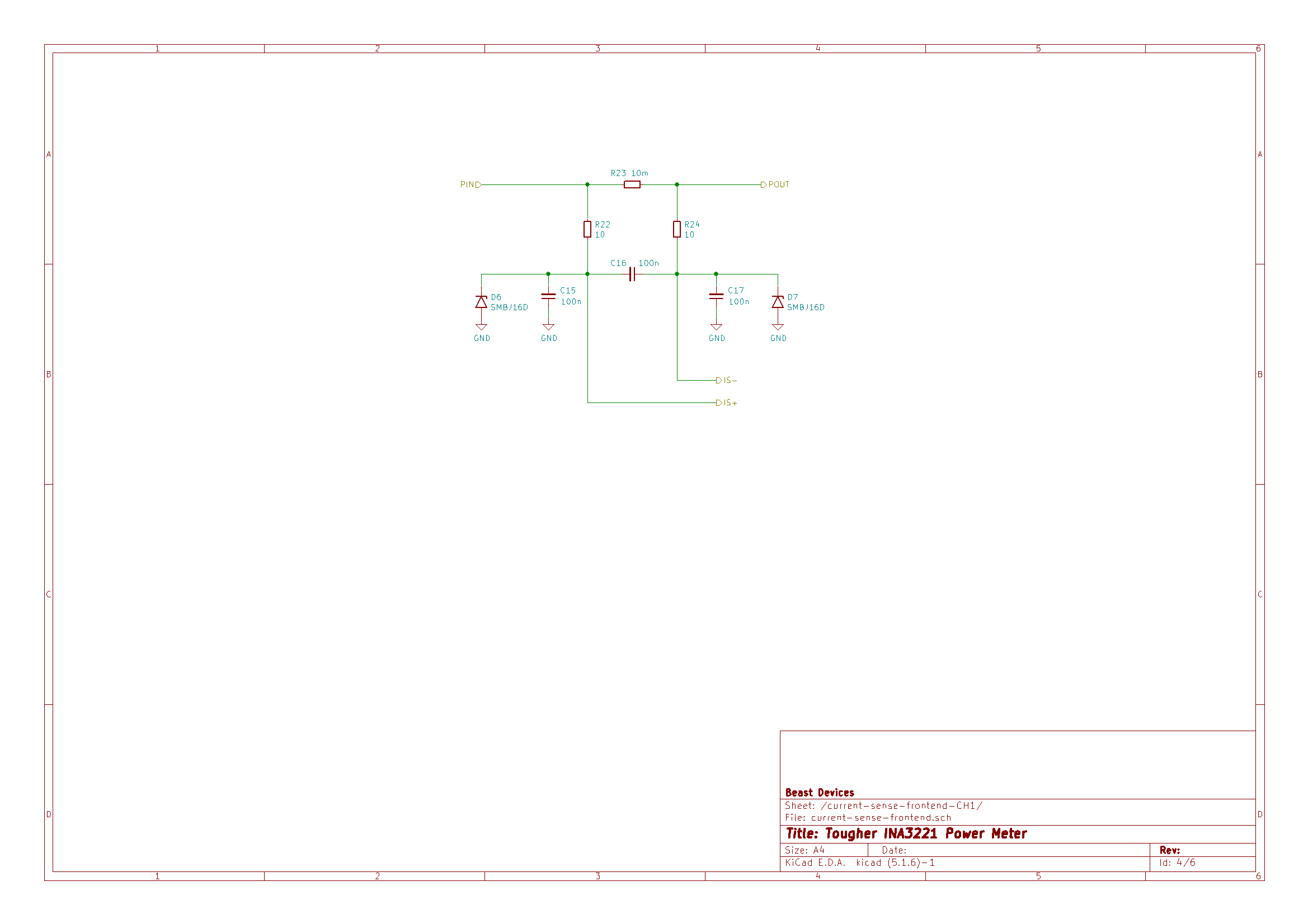
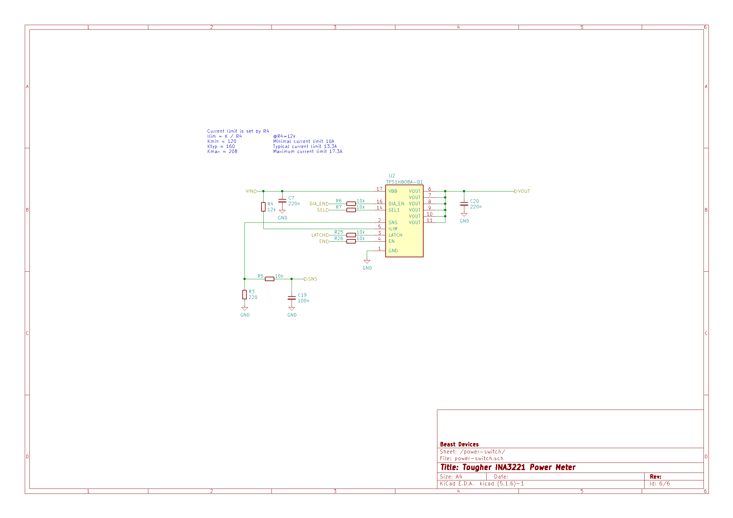
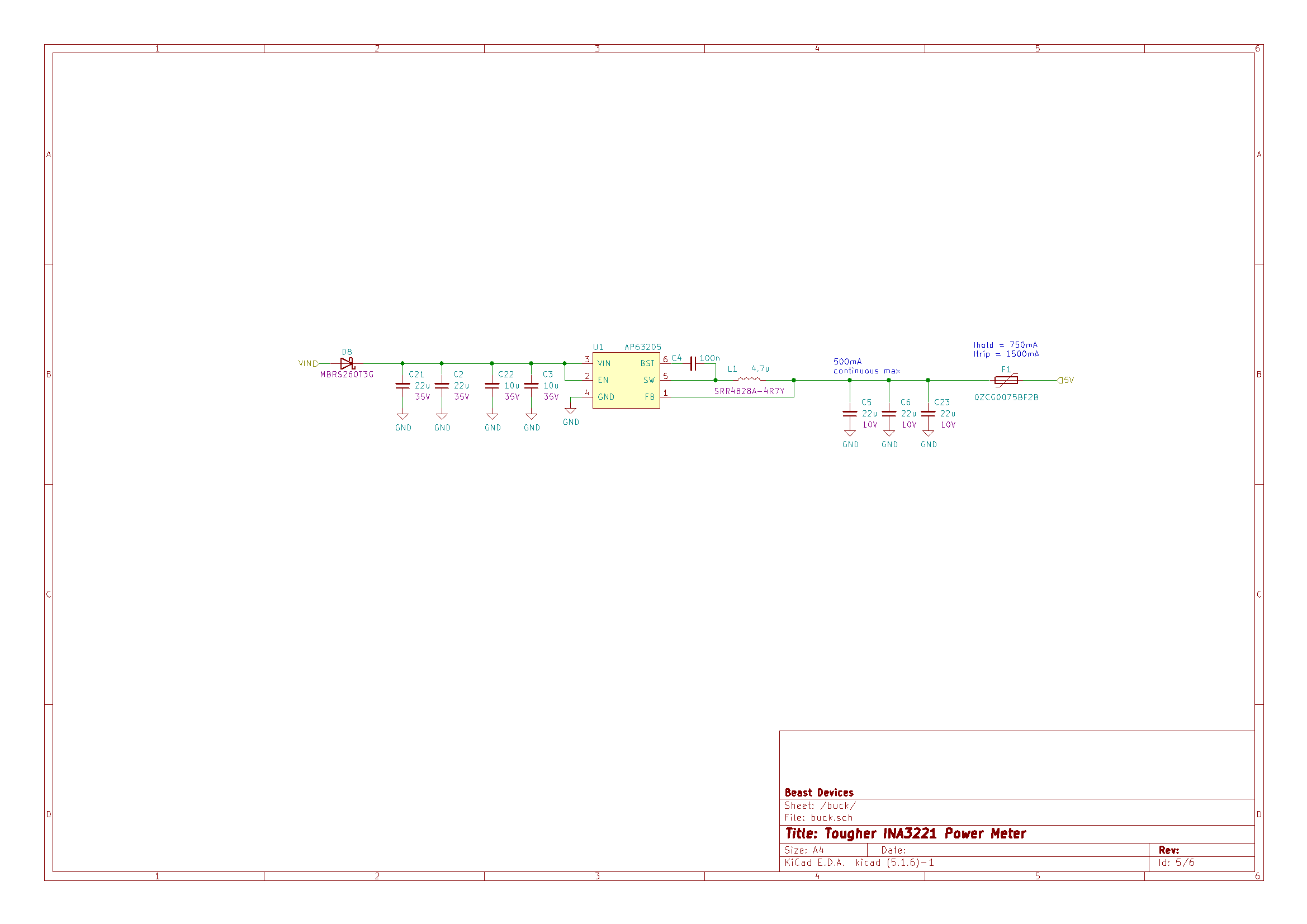
The schematics
09/05/2020 at 13:15 • 0 commentsMy first ever schematics in KiCAD is finished. It was a bit difficult to get used to it after working mostly in Altium and CircuitStudio.
![]()
![]()
![]()
![]()
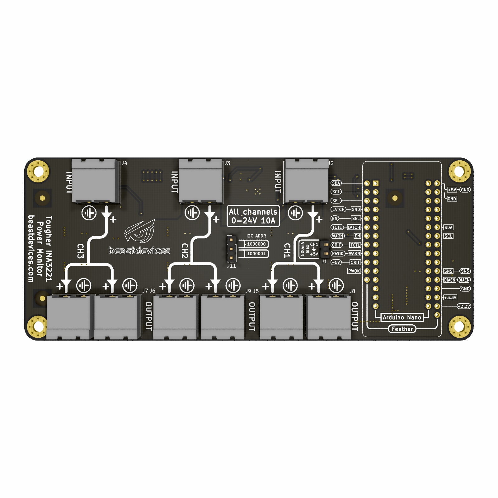
Tougher INA3221 Power Monitor
Triple-channel power monitor based on INA3221. Compatible with Arduino Nano and Feather.