-
Power Supply Issues, cont'd
09/20/2021 at 15:45 • 0 commentsIn the previous log, I mentioned that the system was particular about the source of the 12VDC input. With certain wall warts and power bricks, the +12V would not turn on. In some cases, it would destroy the buck regulator chips on the power supply board.
The new power supply PCBs came back from OSHPark, and I built the first one up this weekend. After talking with a friend who knows a lot about power supply design, I decided to replace the inductors in the input power filter with simple wire bridges. Testing the new board with a variety of 12VDC sources, the system will power up with all of the sources that it had problems with previously. It looks like the regulated wall wart power supplies do not like powering up into an inductive load. Most of the wall warts available now, are the regulated variety, so this is a useful piece of information.
I did a preliminary set of tests to see if removing the input filter inductors is going to cause more conducted emission problems from the power supplies. To perform these tests, a circuit called a Line Impedance Stabilization Network (LISN) is inserted between the power source and the thing being tested. A spectrum analyzer is connected to the LISN to observe the Radio Frequency energy coming out of the thing being tested.
I used two of the power supply boards, one with the input filter inductors populated and one with them bridged out. A 5 Ohm power resistor was used as a load.
At very light loads, the input filter inductors made a large difference. The signal levels below 1.5 MHz on the board with the filter inductors were about 50dB lower than the board without the filter inductors. I didn't test above 1.5MHz on this test setup.
The regulator board has two separate regulated outputs, 5V and 3.3V. Two separate regulators provide these outputs.
With either the 5V or 3.3V output loaded with the resistor, the filter inductors did not make a lot of difference between 1.5 and 11 MHz.
Between 11 and 50 MHz, the signal levels out of the board without the filter inductors are about 12dB higher than the board with the filter inductors. The filter inductors are clearly doing something (beside blowing up regulator chips).
09/23/2021 As an added scrap of conformation on the inductors, I have another filter/regulator power supply board that uses a completely different switching regulator chip but a similar input filter. This board would not operate on wall warts either. I built up one of these boards this week with the filter inductors bridged out and this new board works fine with the wall warts that I tested with.
-
Power Supply Issues
08/14/2021 at 00:55 • 0 commentsThis clock has been operating just fine for the last 11 months until about a week ago. We had a power outage due to an electrical storm. When the power shut down, it oscillated on and off rapidly for about 30 seconds. Apparently, this fried the buck regulator chips on the power supply board and sent +12V out on the 3.3V and 5V rails. The stuff running on the 5V rail had LDO (linear) regulators between the 5V supply and the loads, and they survived. The display driver boards were running directly off the 3.3V rail and when it went to 12V, all 9 of the display driver boards were killed.
Rather than repair the display driver boards, I have substituted different design driver boards from the work that I did on the display drivers last year. This was less expensive and fairly simple to do. The mechanical mounting plate for the displays needed to be re-designed and fabricated. The replacement display boards use the MAX7221 driver chips, so they have a SPI interface rather than the I2C interface of the original boards. The cable change for the SPI interface was simple to do. The display driver software for the MAX7221 chips is substantially different below the top level than the I2C software, but the top level function calls for the driver library are almost identical. I swapped in my replacement library and only had to do minor edits in a few spots. The MAX7221 drivers run on +5V, so the whole system is operating on +5V now.
The most difficult part was to get the physical layer SPI drivers to work. My driver library calls the Atmel/Microchimp ASF low level drivers to deal with the hardware interface. The ASF libraries have been a big disappointment: the documentation stinks and the code is strangely architected and buggy as hell. The serial driver was so bad that it was easier to code my own than use the ASF library. The SPI functions are close to that point.
Another project was running on the same design filter/regulator board as this clock was, and it also failed in a similar manner in this storm. Since both systems failed, there is a regulator board design problem. Now that the whole clock system is running on +5V, I have another filter/regulator board design using different regulator chips that may be suitable. The switching regulator on the substitute regulator board is an older design which runs at much lower frequency than the one being replaced. Right now, there are significant noise spikes on the +5V power rail, and when using the 12V wall wart power supply that the system was running on, the GPS is having problems getting a fix. When running on a good quality bench power supply, it is OK. The noise spikes may be from the older regulator, or the different display driver chips. This is still to be determined.
I think that I am not done with the power supply issue. In addition to fixing the noise problem, I need to look at adding an overvoltage crowbar circuit or a hot swap power controller between the 5V regulator and the rest of the system. This is to protect the system from similar failures in the future. Shorting the switching transistor is one of the most common failure modes on a buck regulator system. The rest of the system needs to survive this.
Hot Swap power controllers make excellent protective devices. Originally designed to go on PCBs that get inserted into a powered up system like a server rack and protect the system and the PCB from transient events related to plugging in the PCB. They have undervoltage and overvoltage sensing to disconnect the PCB power from the input power supply. They have overcurrent sense to disconnect the output from the system in the event of a problem on the PCB. Lastly, they have a linear "soft start" feature to control the current while the capacitors on the PCB charge up to the system voltage.
Once I have the power supply problems sorted out, I will edit this log and post the results.
9/10/2021 Update

Power Supply Board Schematic
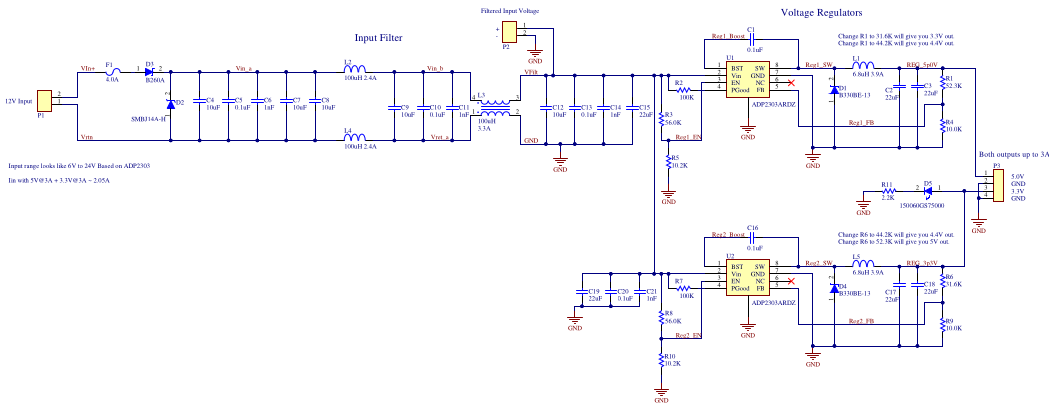
Here is the schematic for the power supply board that has been causing problems. The capacitors and inductors in the upper left quadrant of the schematic are all part of an experimental input filter. The connector P1 is the DC input to the system. It goes directly to a barrel jack on the case of the clock. The purpose is to prevent noise from the switching regulators from getting out onto the external wiring and radiating from there. To a lesser extent, it is also to prevent noise from entering the regulators from the outside world, but the environment that I have been running these boards in does not have a lot of opportunity to pick up noise outside the system.A couple of things that I have discovered while looking through this system:
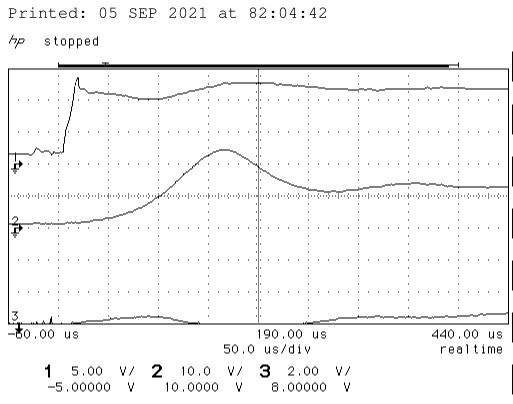
1) The inductors in the input filter are capable of generating a pretty stout transient when the external power supply is plugged into the box.
2) The saturation current on the regulator inductors (L1 and L5) needs to be above the max current that the regulator can switch.

Ch1: DC input across P1 Ch2: Output of the filters across P2 Ch3: Output voltage of the 5V regulator The scope shot above shows the voltages at the input of the board, the output of the filters and the output of the 5V regulator when power is applied to the board via P1. The input voltage is 12V and there is a modest spike when the energized 12V supply is connected to the board. Looking at the filter output, that modes spike goes up to 25V or more. The data sheet absolute maximum input voltage on the ADP2302 regulator chips is 24V. It is not difficult to imagine that transient on the filter output exceeding that value and killing the regulator chips. The output of the 5V regulator does not start coming up until after the transients have settled down.
There are 2 possible fixes for this problem. The simplest is to remove the input filter inductors (L2, L3, L4) and bridge the sites with wire or metal strips. This will reduce the filter roll off, but has a high chance of solving the transient problem. I need to build a jig to measure the conducted emissions and see if they are acceptable after removing the inductors. It would also be interesting to see what the emissions look like before removing the caps too. The second fix is to put a voltage clamp like a Zener diode across the filter output. There is already a clamp across the filter input (D2), and that is likely why the input voltage transient only goes up to about 16V on power up.
An additional advantage of removing the filter inductors is that the inductors are expensive, about half the cost of the complete board.
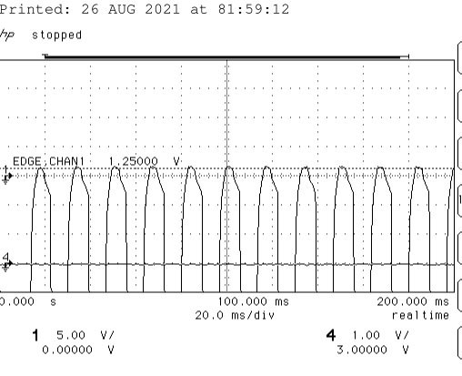
When testing the power supplies, some 12V 1.5A wall wart power supplies would not successfully power the system. In some situations, they would destroy the regulator chips instantly, and in some situations, they would just sit without the input voltage coming up far enough to start the regulators. Here is a scope shot of the wall wart output voltage and current while attempting to drive the regulators.

CH1: DC? Input Voltage Across P1 Ch4: Current into P1 The channel 1 trace is the wall wart output voltage and the channel 4 trace is the current going into P1. The input voltage is swinging more than 20V below ground on these pulses. The blocking diode D3 protects the board from these negative pulses. There is some kind of interaction between the wall wart and the LC input filter. I tested the wall wart with a resistor capacitor load and it sucessfully comes up to its rated output voltage in that situation. I can only assume that the LC filter is causing problems with the wall wart regulation during start up.
Reading the data sheet on the ADP2302/3 regulators, there is a mention in the section on inductor selection that suggests that the saturation current rating on the regulator inductors (L1 and L4) should be above the maximum current output of the chips in some situations. The regulator current is under 1A in normal operation. During startup, it can get higher while charging the capacitors spread around the system on the power supply rails. I have not observed it going above 1.5A. The first regulator inductors I tested were rated at 2A. The reliability of the board with these was very poor. I swapped in some inductors rated at 4A and things worked much better. This clock operated for many months with those inductors in place. The peak current output of the switch from the data sheet is 6.4A. I found some inductors rated at 8A that are close to footprint compatible. It took a little scraping of the solder mask to fit the new inductors on the existing PCB.
I revised the board to easily use these new inductors and include clamping diodes on the filter output voltage and the regulator output voltages. The clamp diodes on the regulator outputs are intended to blow the input power fuse F1 which has been downrated to 1.5A in the event that the regulator chips short again.
-
Input Power Filter Testing
10/05/2020 at 18:29 • 0 commentsFrom the Project Description:
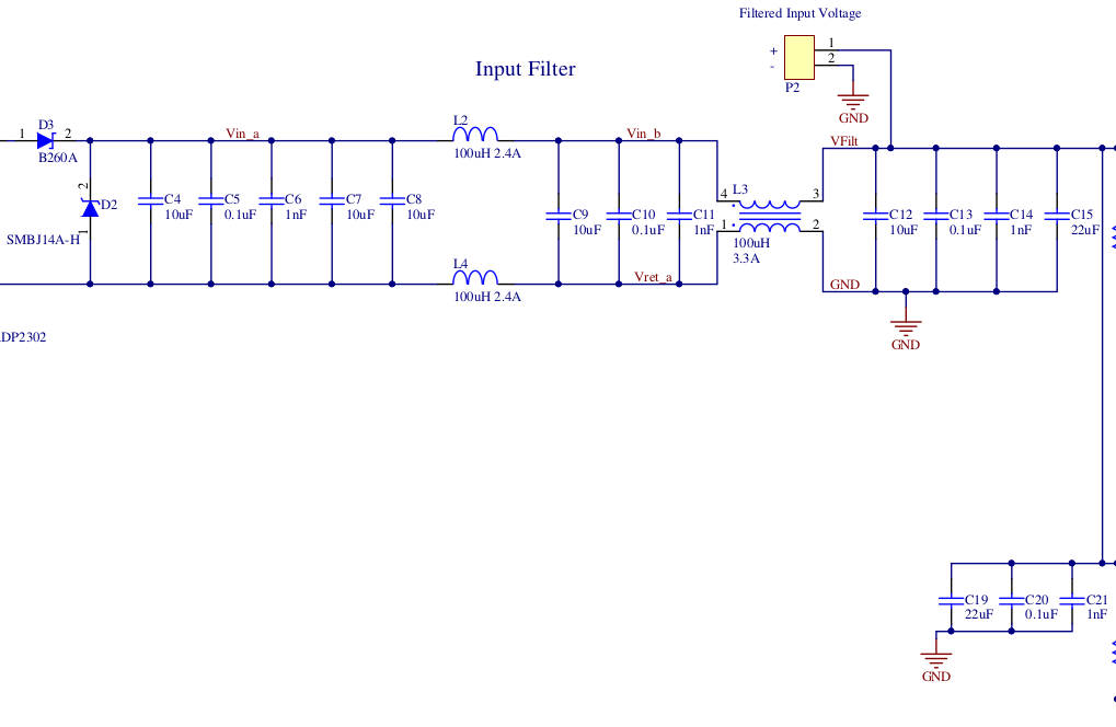
"There is some debate about the use of multiple parallel capacitors of different values in filters. The parasitic inductance of capacitors mean that large capacitors that are capable of supplying the instantaneous current demands stop looking like capacitors at disappointingly low frequencies. Electrolytic capacitors are really bad in this respect, but the ceramic chip caps suffer from it as well. Lower value capacitors have lower parasitic inductance, so they continue to behave like capacitors to higher frequencies, but won't supply much energy. The most obvious solution to this is to put some smaller value chip caps in parallel with the high value caps in the expectation that the high value caps will supply the instantaneous current while the low value caps will provide low AC impedance to higher frequencies. I have seen several competent people claiming that this idea does not work. I have also heard some people claiming that it does work. I want to see for myself, so the input filter design used here has sites for a range of capacitors.
The new PCBs came back from OSH Park on Friday. In order to test the behavior of the input filter and to attempt to determine if the parallel capacitors spanning a range of values contributed to better high

Input Filter section of the Filter/Regulator board frequency filtering, I populated all of the inductors on the board and just the 10uF caps C4, C7, C8, C9, C12
and tested the board with my home built Scalar Network Analyzer, sweeping from 100KHz to 30MHz.
Next, I populated the 22uF caps C15, C19 and repeated the sweep.
Then I populated the 0.1uF caps C5, C10, C13, C20 and ran another sweep.
Finally, I populated the 1nF caps C6, C11, C14, C21 and ran the last sweep.
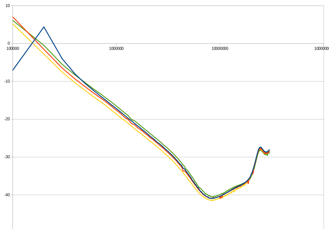
The results of the 4 test runs were almost indistinguishable from each other. This is the behavior that I would expect if the individual caps just combined into one capacitor "blob". It is possible that 30MHz is not high enough to see the individual capacitors contributions, but I am not set up to test to higher frequencies right now.

Plot of Amplitude in dB vs Frequency through the input filter. The plot shows Attenuation in dB on the Y axis and Frequency plotted logarithmically on the X axis.
The blue trace is with only the 10uF caps and the inductors populated. I am not certain what the extra peak is around 200KHz. The traces appear to converge as the frequency increases. I was expecting that the traces would start to diverge around 5 to 8MHz, as that is where the manufacturers data sheets show the parasitic effects becoming dominant on the large capacitors.
I believe that the minimum around 8MHz is the parasitic capacitance in the inductors L2 and L4 reducing their effective impedance. This is supported by the fact that all of the plots show a very similar feature.
Until I can test this farther, I am going to assume that paralleling a span of capacitor values does not work as I hoped.
-
Put the covers on after powdercoating
09/21/2020 at 00:09 • 0 commentsThe project looks a lot more finished after powdercoating the case. The case is formed out of 0.030" 5051 aluminum. This case design does not require any welds. Nutserts were used on several of the machine screw holes because it would be difficult or impossible to get a conventional nut into the case.
The cable coming out the top of the case is for the GPS antenna. Right now, the little patch antenna is not working to get a fix in my shop. A higher gain antenna with a view out the window is on the other end of that cable, and it works fine. I will get a higher gain patch antenna to sit on the top of the case and see if that is sufficient to get reliable fixes inside the house.
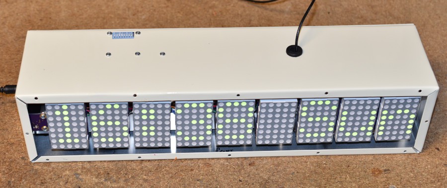
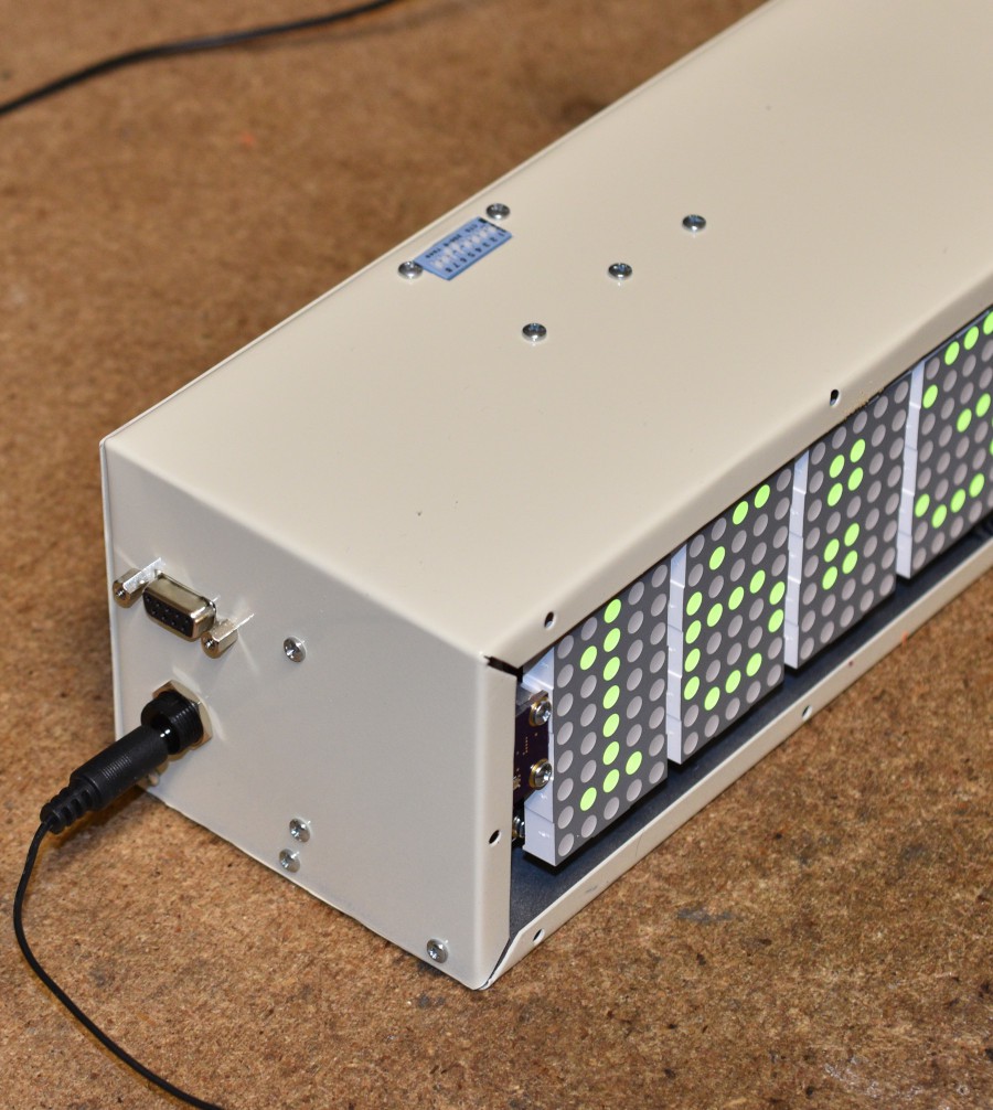
Front and Top View End and Top View The DIP switch, Debug console port and power connection are visible in the end and top view shown.
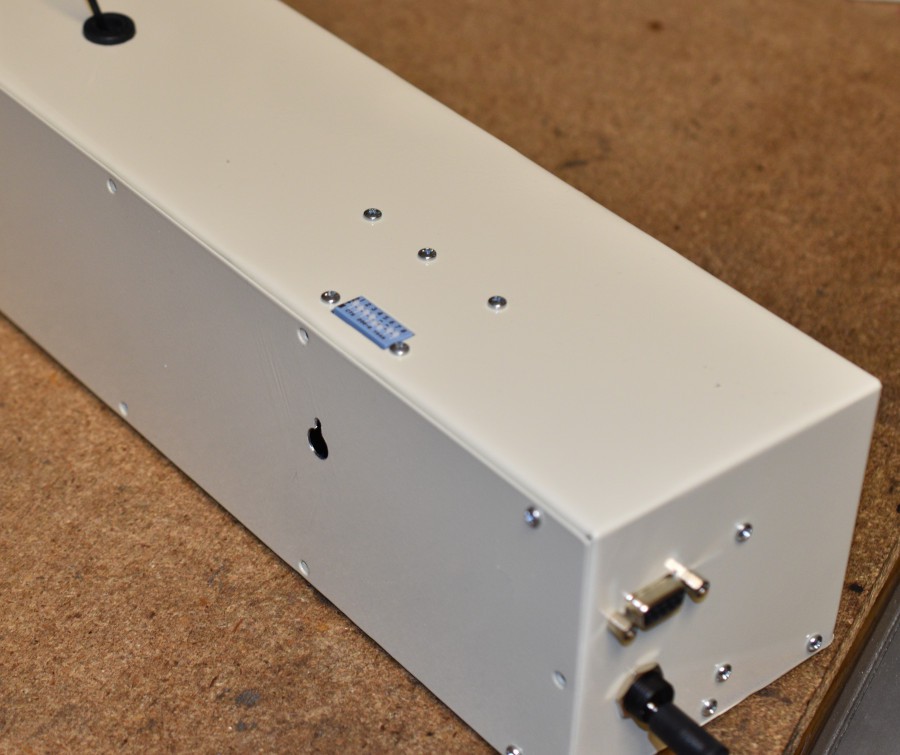
Rear Quarter View The slots in the back cover will be used to hang the clock on the wall.
The last step is to put a neutral gray filter on the front of the box. It should increase the contrast and conceal some of the details inside the box.
Finally, I got the plastic for a cover/filter for the front of the box.
Front View of Display, through the gray cover/filter
GPS Driven Clock
This clock displays the time and day of the week directly from a GPS receiver.
 Bharbour