Christoph
-
The result
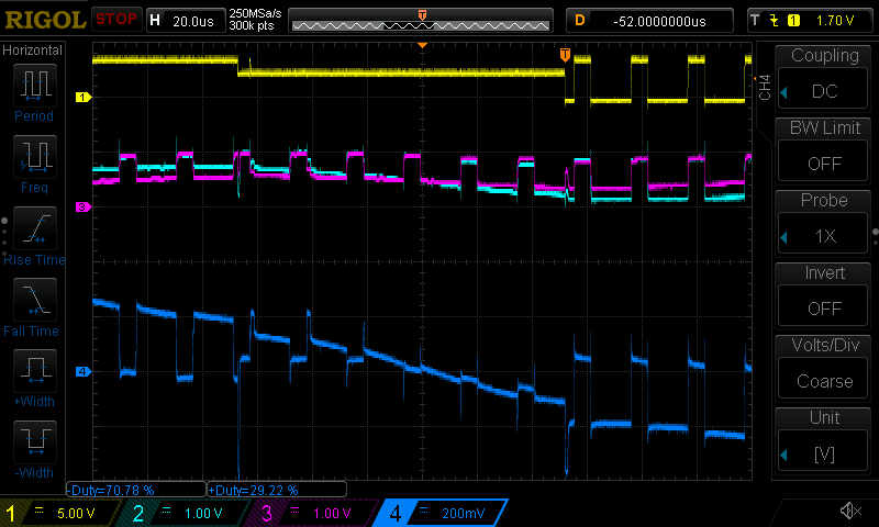
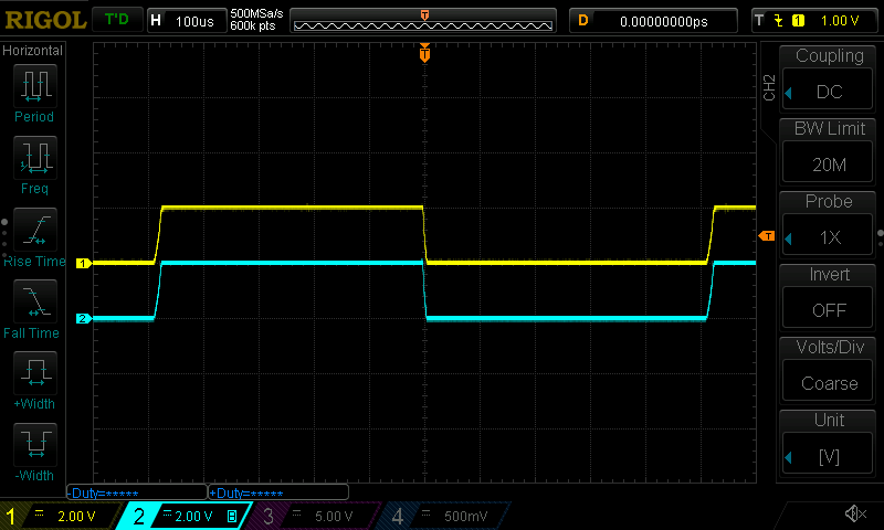
10/13/2020 at 18:19 • 0 commentsThis is what I started with - DS1054Z math to show the difference of two signals:
![]()
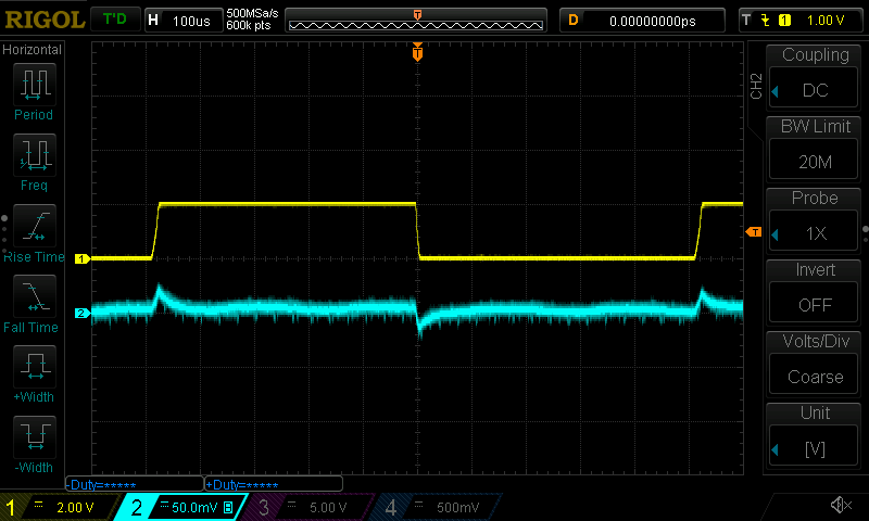
With the differential probe, I can get a better signal representation and get one input channel back.
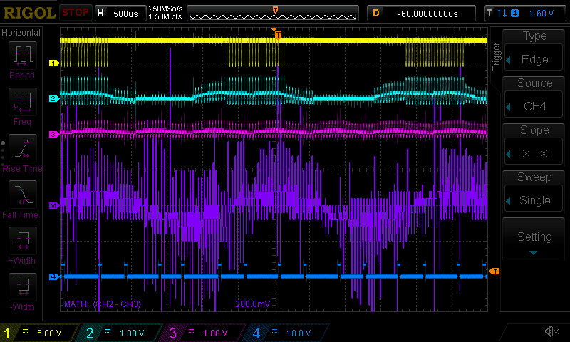
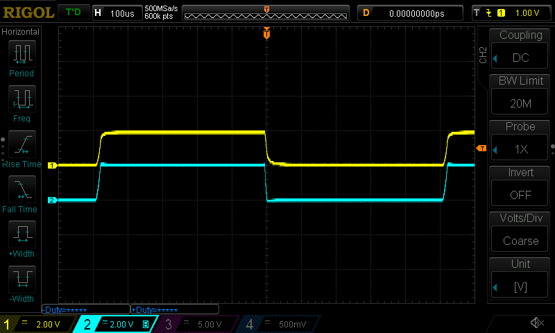
Here's a sample screenshot that actually shows what the probe does:
- supply voltage to motor: 5V, duty cycle about 60%
- Ch1: 3-state PWM input to motor phase A
- Ch2: bemf from phase A, through a 10k/2k2 voltage divider
- Ch3: virtual center (all phase feedback signal tied to a common node through 2k2 resistors)
- Ch4: Ch2-Ch3, using the diff probe
![]()
It has been a very pleasant journey into the analog world for me. Thanks Bud!
-
Compensation procedure
10/13/2020 at 17:37 • 0 commentsBud describes the compensation procedure in his project's details (see here: https://hackaday.io/project/169390-a-10x-100mhz-differential-probe/details), and the description is good, but it doesn't provide any scope shots of the process. To compensate the probe, you need a square wave signal at two different voltages. I used my bench PSU, an IRLML6344 (NFET) and a 1k resistor for that. The FET's gate is driven by my scope's square wave output.
Step 1: cancel DC common mode error
Set the PSU to 20 V to get a 20 V square wave on the FET's drain. Connect both probe inputs (+ and -) to the FET's drain. You'll see something like this:
![]()
(Ch1 is the 20 V square wave, Ch2 is the probe's output).
We want the flat parts of Ch2 (left and right of the plot's center) to end up on the same level, by adjusting R11. The result:
![]()
Step 2: match positive signal path AC gain to DC gain
Lower the square wave voltage to 2 V and connect probe + to drain, probe - to gnd:
![]()
The goal now is to get rid of that little overshoot at the top of the rising edge by adjusting C5. We want the top and bottom to be as flat as possible. If you can't do that with C5, change C7 to move the trim cap to the right range.
Result:
![]()
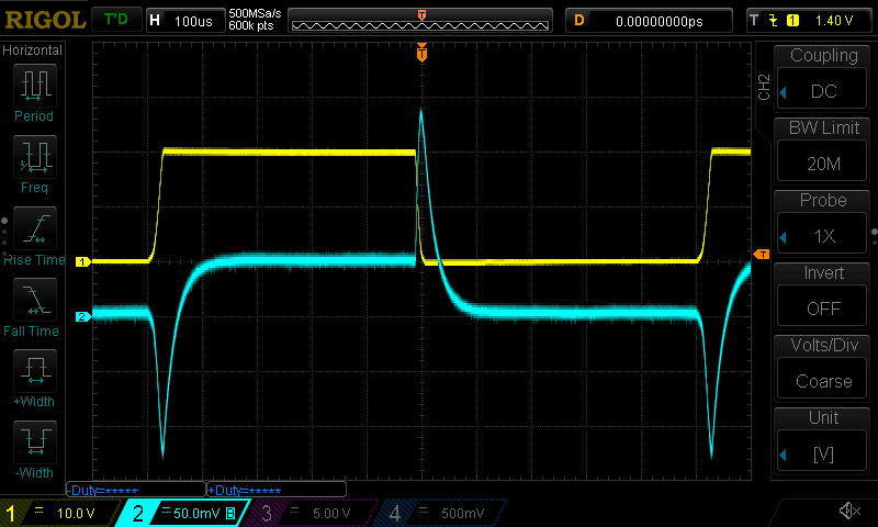
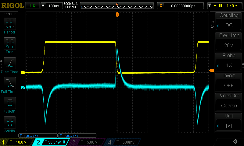
Step 3: match AC gain between positive and negative signal paths
Back to a 20 V square wave, both inputs connected to the FET's drain:
![]()
Those peaks will now be removed by adjusting C10.
Result:
![]()
It's not perfect, but the probe reacts to just about anything in its surroundings.
That's it. The whole procedure took about 10 minutes.
-
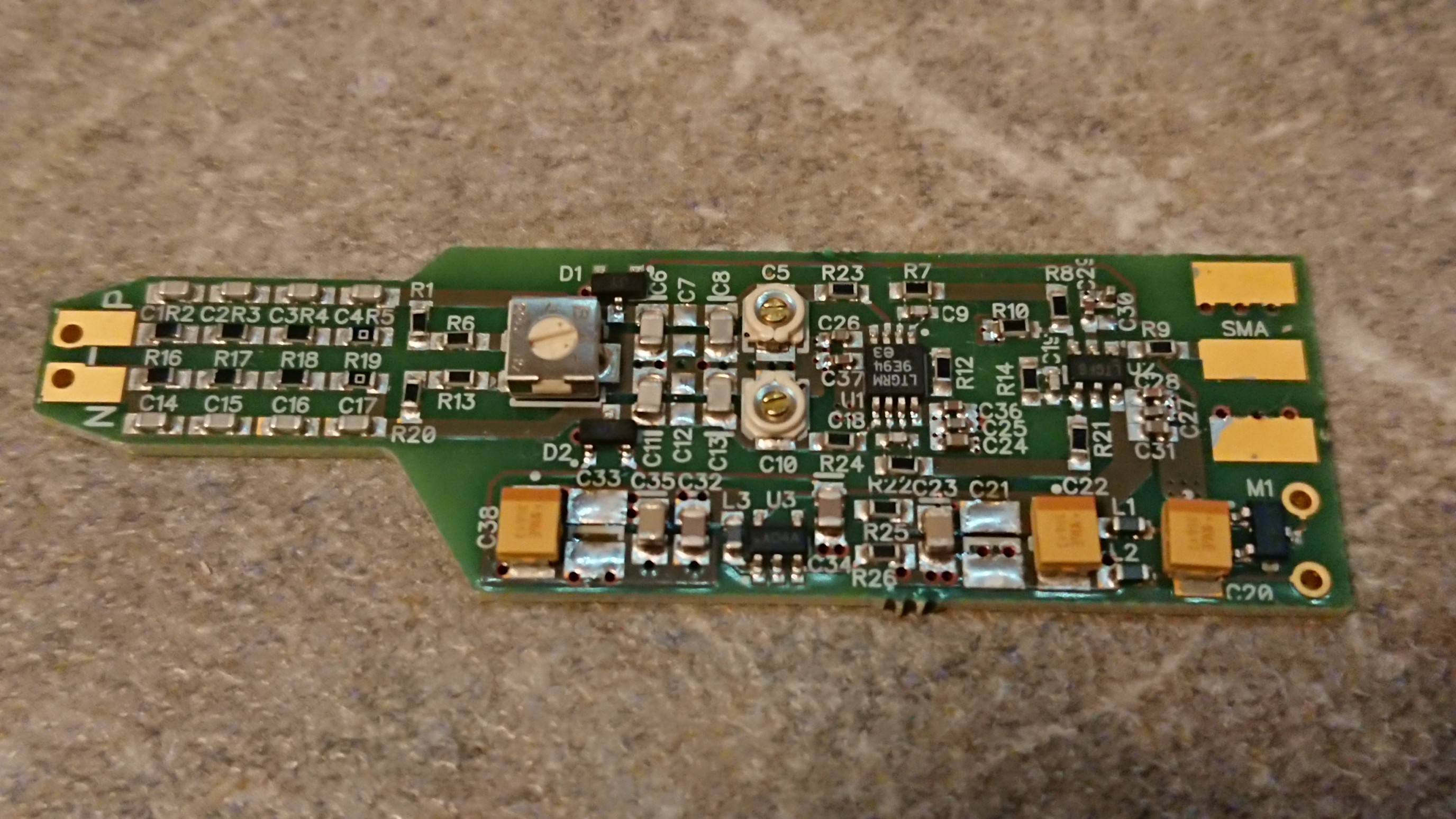
Assembly
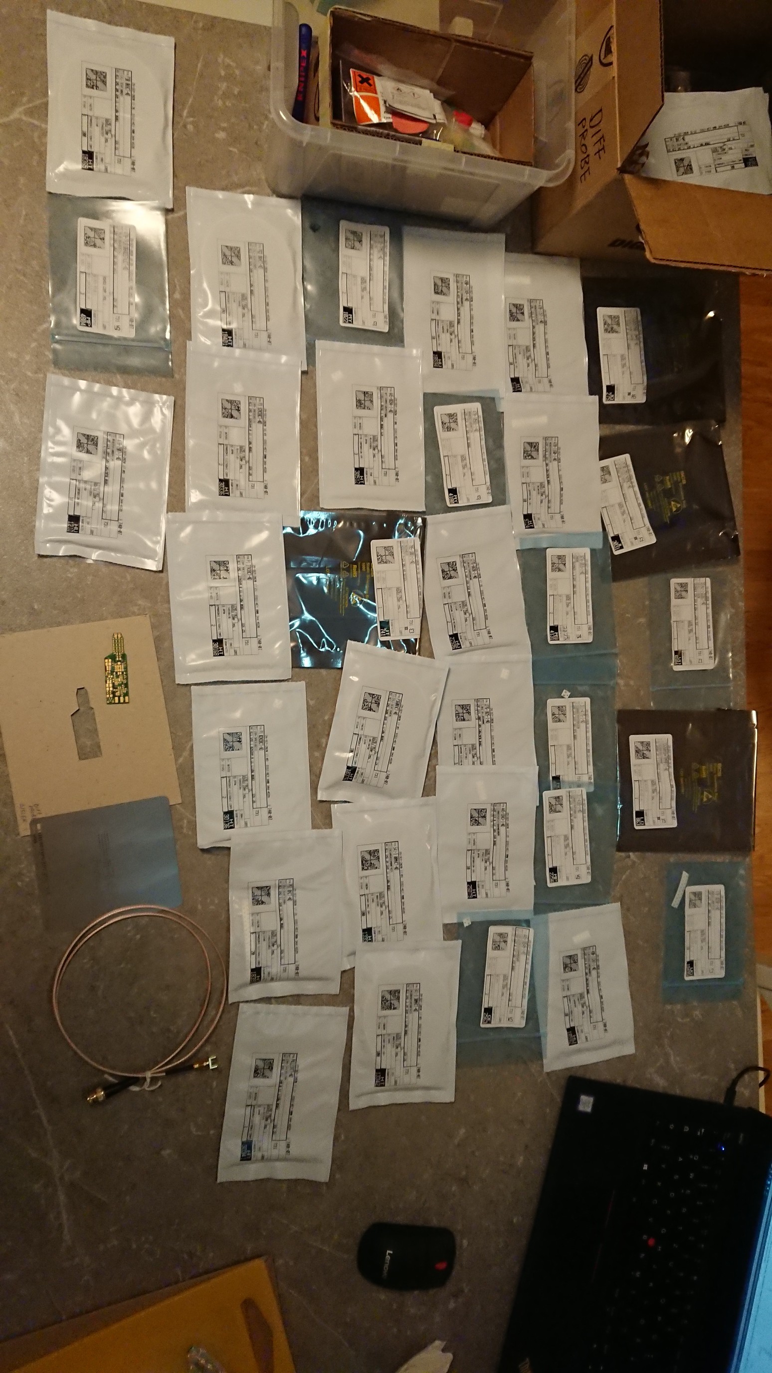
10/13/2020 at 17:15 • 0 commentsNo big surprises here: Since many of the parts have very specific values, tight tolerances and low temperature coefficients, I could only use 2 resistor types that i had already. So I ordered the rest from digikey and ended up with a huge pile of almost empty bags:
![]()
PCBs and stencil are from Aisler, as well as that piece of 1.6 mm cardboard (I love that!).
The land patterns seem to be made for hand soldering, so I expected the 0402s to tombstone. One did:
![]()
That was fixable, and the large tantalum cap in the lower right corner needed a little touch up. Other than that, everything went well. Assembly took about 100 minutes from cutting the opening in the cardboard to reflowed PCB.
Since I wanted to power the probe from a 5V USB port, I added a USB cable. Of course, it had 5V on the black wire and ground on the red one, but M1 is there to keep such a mistake from damaging the probe.
-
Changing the attenuator to make it a 1x probe
10/13/2020 at 16:56 • 0 commentsSince the voltages I'm dealing with are not as high as Bud's, I decided that I wanted to modify the input attenuator from 1:250 to 1:25. This had to be done for the resistors and the capacitors.
There was a caveat though: Bud found that the layout introduces some error in the capacitive divider, effectively lowering the capacitance of C1...C4 by 7.5 %. I've taken that into account in my calculations and the result was spot on (pure luck to be honest because I didn't place the smallest cap that was meant for tweaking the result).
I've put the results into a zipped xlsx file that can be found in the project files.
A 1x, 100 MHz, 35 V common mode diff probe
I needed a differential probe for BLDC motor ESC development and adapted Bud's design for my needs