-
1Step 1
![]()
Warning: hacker construction project
If you are interested in making something like this, be warned. This project is a total hack job and will not run on any out-of-the-box hardware I am aware of. Development boards are available, but would require modification or additional peripherals to be a Tickernut clone. Possibilities include the Ethernut 2.1 or maybe the smaller MMnet01, either of which would need a CPU upgrade to an ATmega2561.
Thanks to the portable nature of Ethernut, the Ethernut 3 or 5 boards with ARM CPUs are probably a better choice and should only require minor code changes. The rapid prototyper would probably be best served by a Raspberry Pi running a subset of the application code, whereas the AVR fan might consider an Arduino Mega with a RAM expansion and an ENC28j60. At the end of the day, the hardware is not important.
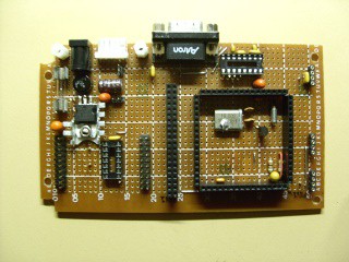
I built mine on protoyping board following the Ethernut 1.3g reference design. At the start I was not sure if the design would prove capable enough, and as it turned out, it wasn't. Upgrades during development included the addition of an SD card, a move from the ATmega128 to an ATmega2561, altering the address decoding to make a full 40K RAM available rather than 32K and changing 434Mhz radio modules for the 2.4Ghz nRF24L01+. Even then it took a lot of trickery, training and some sleight-of-hand to make it do as it's told.
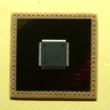
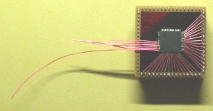
I was inspired to this approach when I came across this device, demonstrating to me that connected computers could be hand made from junk and wires. I was mightily impressed by the home brewing resourcefulness of this creation and resolved immediately to follow in kind.
For the display I had nothing to suit my desires, so the cheapest, most cheerful LED arrays were sourced and purchased from China. Wiring them together in a useful fashion was the single hardest task of this build.
All up it has been a challenge that pushed the boundaries of my abilities and has brought me both great elation and deep despair. I now have invested so much effort and time into seeing this mad device work I would be heartbroken were it to fail beyond repair, which on several occasions it seemed to me was precisely what had happened.
But despite all the setbacks and obstacles the system now works reliably well. We here are now right up to date with all the latest.
![]()
-
2Step 2
Lexitron circuit design and hardware:
![]()
LED display:
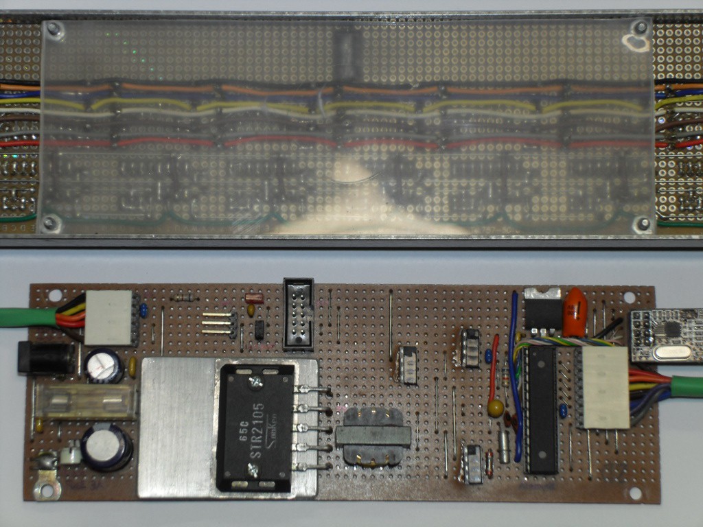
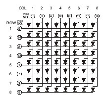
The display is constructed using Red 8x8 square LED matrix displays, each containing 64 LEDs wired in a square grid with the 16 column and row pins available out the base. It is designed to be used in a multiplexed mode, with just eight or less LEDs illuminated at once in a row or column that is only energised briefly as the whole array is swept through quickly like a raster.![]()
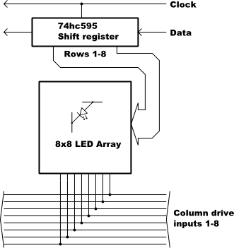
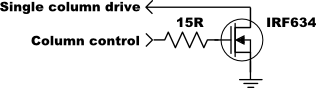
In this design each display module gets it's own column driver to act as a current source allowing the row connections to be shared along all the display modules into a single set of current sink mosfets.
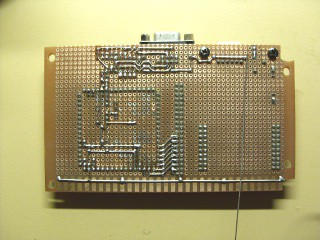
The display control circuit is a multiplexed column design using cascaded shift registers. The layout is organised into 8x8 cells, each with their own shift register. In each cell the data in the shift register energises the rows while the chosen columns of all cells are parallelled together to be selected by 1 of 8 mosfets. This design requires one chip, one capacitor and eight resistors with each 64-LED display module, and one set of eight power mosfets with gate resistors for the whole display.
![]()
This diagram shows the layout of a single display cell. There are 20 of these, the output of one feeding to the input of the next. Besides power consumption there appears to be little practical limit on the number of these cells that could be cascaded. Not shown is the eight 470R current limiting resistors in series with the row drive connections. Also not shown is a later modification to remove a faint background illumination where the Latch Clock was brought out and series connected like the existing Shift Clock for sharper control.
![]()
Current consumption of the whole display is potentially quite substantial, even with each LED drawing only 10mA turning every LED on at once would require nearly 13 amps and throw more lumens than a car headlamp! The power supply in the display is only rated at 2A continuous, 3A surge. For this reason, and the fact that the shift registers would be seriously overloaded, it is important that only one column of each array be energised at any one time giving a potential maximum draw of 1.6 amps which remains well within ratings. In practice, the current limiting of the supply regulator I used prevents any issue arising from accidental overloads.
Displaying text has a much lower consumption, on average less than half of the maximum current draw, allowing one to use a relatively small heatsink for the supply regulator. In practice the regulator barely gets warm for normal scrolling text display.
If the power consumption limit is very badly exceeded the regulator's output voltage slumps as it's current limiting protection circuit kicks in. This reduces the microcontroller's supply rail causing it to brown out and release the column drive. This appears to provide crude but effective protection against software glitches, code errors and other accidents.
Radio Communication:
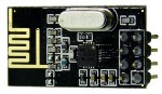
The transceiver is based around inexpensive modules on the 2.4 Ghz band. These modules use the nRF24L01+ chip designed for low power, short range applications like wireless keyboards and mice. They have a host of features like multiple endpoints and auto-ack, most of which I do not use.
This module connects to the microcontroller using the USART, configured for SPI bus mode. It listens for packets from the Tickernut and responds with ACK or data to every one. The link layer includes packet sequencing and automatic retries for a more robust connection.Power supply:
![]()
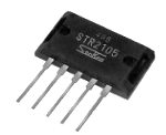
The 5 volt power supply built into the display is using components recycled from an early ink-jet printer IIRC. It is based around a very large integrated regulator, the STR2105. This chip is deprecated, new designs would be better using a more modern IC like the LM2575-5.0 or similar.
![]()
The STR2105 is a 5 volt switch-mode design and requires only an external inductor and capacitors to work but adding trimpot VR1 allows precise output voltage trimming. Despite the size of the device the specifications are quite modest at 2 amps continuous, 3 amps surge. The advantage of such a large package is it has lots of thermal dissipation allowing for a relatively small heatsink in this application.
The external power supply has been borrowed from a very early Toshiba laptop (T1200?) and has an output of 12 volts at 2.2 amps. It is being used without modification and may be returned to the vintage laptop if a suitable substitute is later found.
Display microcontroller connections:
An Atmel ATmega8 was initially chosen for the display mainly because there was one on hand and it fulfills the requirements of being physically small, possessing a hardware SPI interface and supporting a bootloader. This was later upgraded to an ATmega328p for more resources and a second SPI interface.
The SPI interface is well suited to shift data into the shift register chain as it can do this many times faster than bit-banging the serial data out in software and also saves the small amount of code that would be required for this.
The clock source is a 14.31818 MHz crystal, initially chosen to match the Tickernut base station in order to eliminate baud rate errors. Even though this is not a standard baud rate crystal the display and base station's baud rates were the same. With the upgrade to nRF24L01+ modules, this was no longer a requirement and the Tickernut has since been given an 18.432 MHz crystal for improved processing speed.
Due to the use of switch mode power supplies and lots of heavy current switching, extensive decoupling on the supply lines is used throughout the circuit and especially around the microcontroller to ensure the noisy 5 volt supply does not interfere with normal operation.
The awkward choice of column drive connections was mainly dictated by how the veroboard layout evolved. If it had been possible to assign all eight columns to a single port more effort would have been made but as all ports had some pins already in use for their alternate functions it was necessary to share the columns between two ports. This being the case, the bit order became much less important as the column control routine needed to be bit-oriented rather than byte-oriented anyway.
More to come..
![]()
-
3Step 3
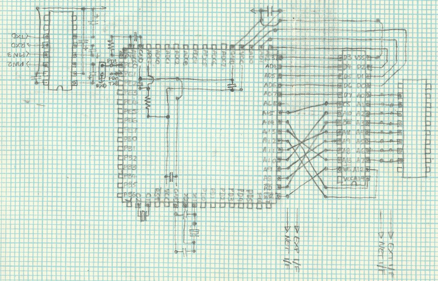
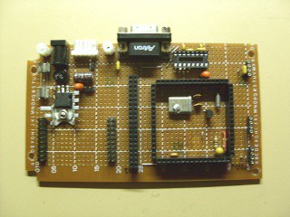
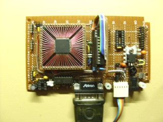
Tickernut circuit design and hardware:
![]()
![]()
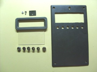
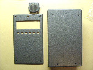
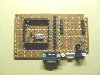
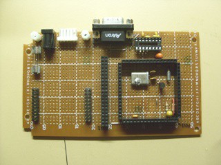
Enclosure:
The motherboard is shaped to fit tightly inside a standard ABS jiffy box which set its limited size. The box has cutouts to expose all motherboard connectors on the left side and a small speaker and antenna has mountings on top.
![]()
The front panel is drilled to accommodate switches and LEDs with a cutout above having a bezel with a transparent window for the alphanumeric LCD. Above that, a window for the infrared remote receiver is covered with tinted perspex.
The motherboard:
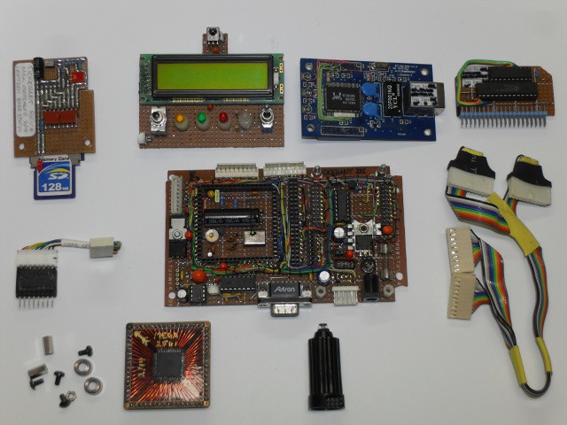
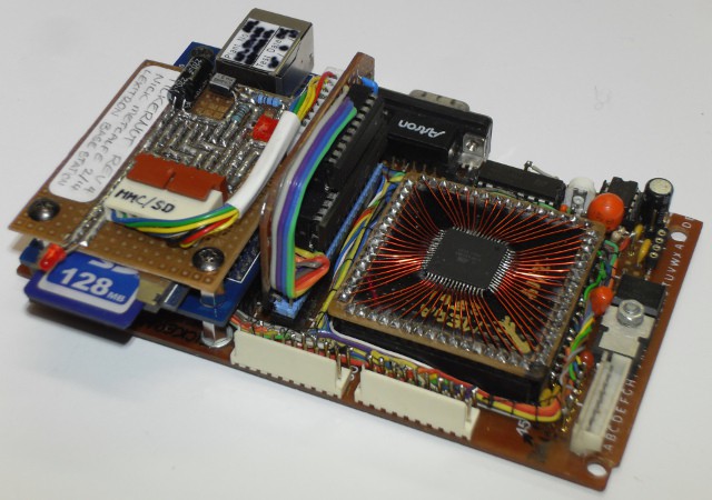
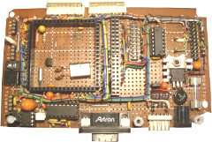
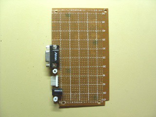
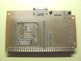
The Tickernut's main board is constructed using phenolic prototyping spot board. The processor, memory and all peripherals other than the front panel controls are mounted on this board. The core of the design is based on Egnite's Ethernut reference design v1.3 rev. G and initially used the same major components, an ATmega128 processor, 32k static ram and RTL8019 network interface. These were arranged into the same memory map as the Ethernut design allowing the firmware to run unmodified.
![]()
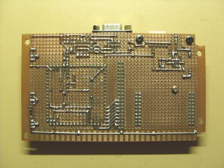
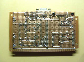
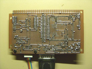
Peripherals located on the motherboard include the memory card, radio modem, audio amplifier, RS232 interface, in-circuit programmer, brown-out monitor, real time clock and power supplies. Much of the circuit wiring is point to point between solder stakes and to keep the wires neat they have been laced together into a loom.
Processor:
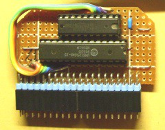
The first processor used was an ATmega128, then one of the higher end devices in Atmel's AVR microcontroller range. It is a great chip, one of my favourite 8-bit microcontrollers. It has 128k of program flash, 4k of static ram, handfuls of on-chip peripherals and is only available in a 64-pin surface mount package.
![]()
The processor was mounted on a hand made breakout board that provides standard spacing between pins to allow the whole unit to socket straight into the motherboard.
Most of the processor's support components including the system clock crystal, 32k real time clock crystal, DS1233 brownout monitor, analog supply and decoupling are mounted on the motherboard inside the area used by the processor socket leaving the area around the outside of the socket free for peripheral connections.
The system was initially clocked at 14.31818 Mhz. This clock speed was chosen as it is an easily obtainable crystal and proved close enough to the Ethernut's original specification of 14.7456 to allow serial communication to work without firmware changes. This proved very handy during initial testing.
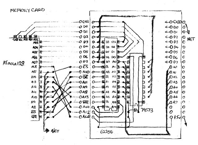
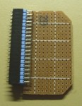
Memory Module:
The memory module consists of a 74als573 octal buffer and 32K of static RAM on a small scrap of prototyping spot board with a large connector that sockets vertically into the motherboard.
![]()
The separate module was constructed to hold the memory because I ran out of space when planning the layout and couldn't find an arrangement that would easily allow the memory chips to be mounted directly on the overcrowded motherboard.
The memory module sits on the processor's external memory bus and functions independently of all other peripherals. It exposes the demultiplexed address and data bus lines from the processor for use by the network module. The memory module is positioned close to the processor and the physical connections are short enough not to require wait states.
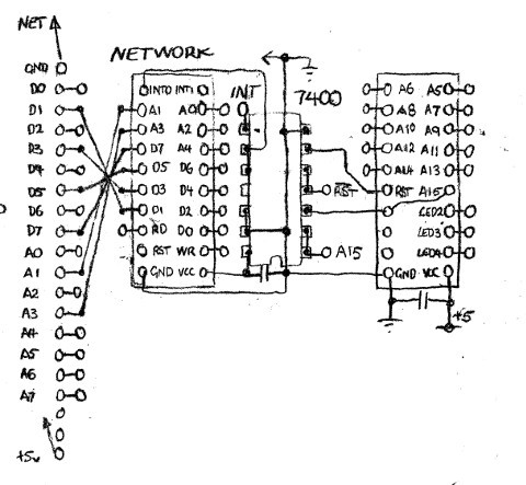
Network Interface Controller:
The network interface module is a Realtek RTL8019 NIC chip on a small carrier board with a crystal, network transceiver and RJ45 connector. This module interfaces power, interrupts, address and data bus through two 20-pin connectors. The network module requires address and data signals from the memory module and will not function if the memory module is not present.
![]()
The network module as I obtained it was wired to only provide the low 5 bits of the address bus but it had many spare pins on the connectors. To avoid extra decoding hardware or unsightly software hacks the network module was modified to make the remaining 11 address bits and 3 status LED signals as well as another reset signal available through the spare pins.
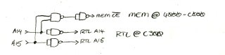
A 74hc00 quad NAND on the motherboard matches the network module's signals to suit the system bus. It is wired as inverters, one on the A15 line to map the NIC's registers directly above the 32K memory space while another corrects the sense of the NIC's interrupt signal before it is fed into the processor's INT5 pin. A third inverter flips the motherboard's active low reset signal to suit the NIC's reset requirements. (Note - this section of the circuitry was later completely rewired to provide the full 40K of RAM, more details later.)
Radio communication:
![]()
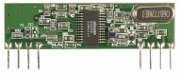
Originally, the transceiver was based around separate inexpensive transmitter and receiver modules on the 434MHz LIPD band. According to their datasheet they were originally designed for garage door openers. These proved to be poorly suited to the job. Communication was so slow and error prone as to be practically useless.
![]()
The transmitter's modulation method is simple on-off keying (OOK), These modules were rated to max out at 5000 bps and seem to work best at 2400 baud. After adding protocol overhead this halves to 1200 baud. The receiver uses a simple circuit known as a bit slicer to recover the serial data stream. This allows the modules to be connected directly to the microcontroller's second USART, RxD and TxD lines. I got them to work in the end but was not happy with their performance at all.
![]()
A major update to the design introduced nRF24L01+ radio modules to the system. These proved far more successful and are able to provide an effective, robust communication link. These connect using an SPI interface, which became available when the CPU was upgraded to the ATmega328p with a USART capable of SPI.
Audio Amplifier:
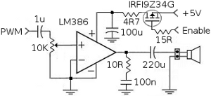
The audio system is driven by a pulse width modulated signal from the microcontroller's second timer on OC1B (PB6). The modulation frequency is high enough to not require filtering. The PWM is ac coupled through a volume attenuator before being fed to an LM386 audio power amplifier. The output of the amplifier is stabilized by a Zobel network and is made available to the speaker through a connector on the motherboard.
![]()
The power supply for the audio amplifier is somewhat choked by heavy decoupling and is below the LM386's minimum operating voltage specification of six volts. For these reasons the audio output clips sometimes and could hardly be described as hi-fi.
![]()
Fortunately the TickerNut's enclosure with the mylar squeaker baffled in the top turns out to be an effective resonator and the squeaker does not need to be driven full blast to be heard loud and shrill. This allows the underpowered amplifier to be driven at a level it can easily sustain. Announcements and speech are clear and legible and easily loud enough to require a volume control.
In the original design, interference issues meant the amplifier could not produce sound while the radio modem was in operation. After the upgrade and with better audio drivers the system is now virtually noiseless all the time and sound is pretty much seamless without clicks or pops.
Brownout Monitor:
The main 5 volt supply rail is monitored by a DS1233 Econoreset. This chip is conveniently packaged in a TO-92 enclosure with just three pins which made it a simple matter to connect it to the circuit inside the processor socket area. The DS1233 watches for sags in the supply rail and activates the reset line when a brownout is detected. It also debounces the reset button which is located on the front panel.
![]()
The microcontroller includes it's own brownout detection circuitry but having the external monitor ensures the network module is always in a known state when the processor comes out of reset.
ISP programming port:
The processor's in circuit programmer is accessible through the serial RxD and TxD lines in combination with the SPI clock and system reset line. These four signals are made available along with earth and jumpered power over the 6-pin Atmel ISP socket which is exposed through a cutout in the case. Another jumper isolates the on-board power supply allowing device powered and device powering programmers to be selected.
![]()
The microcontroller's ISP shares it's serial communication pins with the first RS232 port. To prevent the RxD output of the serial line receiver from interfering with the programmer's MISO signal it is coupled to the shared RxD line through a 4.7k resistor. This allows the serial port to function normally until a programmer is connected. The programmer can easily override the weak serial signal and control the processor without trouble although anything connected to the serial port gets bombarded with nonsense during programming.
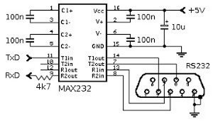
Serial Port:
The RS232 communication is used for debugging. In Nut/OS it has been assigned to stdout and stderr making it the default output device for the stdio library.
![]()
The first USART on the microcontroller is level translated through a MAX232 serial line driver and brought out a 9-pin D-sub connector. the CTS and RTS handshake signals are also routed from the MAX232 to the connector but are not connected to pins on the microcontroller as they are not currently needed.
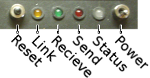
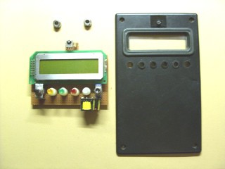
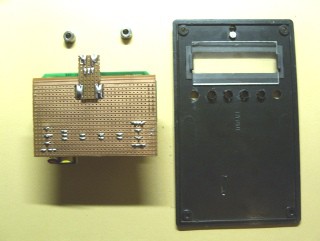
Front panel control board:
The only circuitry in the Tickernut not on the motherboard is on the front panel control board. Peripherals on this board include the alphanumeric LCD display, infrared receiver, bi-colour status LED, network status LEDs, reset button and power switch.
![]()
The front panel is connected to the motherboard by a shaped 20-conductor connector socketed at both ends. The control board is held to the front board by the nuts on the two switches.
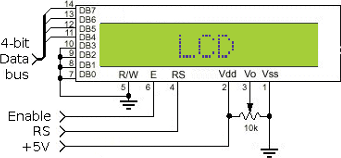
LCD display:
The backlit alphanumeric LCD display is used for reporting device status and debugging. It is a standard Hitachi HD44780 compatible unit with green LED backlighting. The LCD is connected directly to the microcontroller with the 4-bit bus DB4-DB7 going to PD4-PD7 and RS and Enable going to PE2 and PE3.
![]()
To save microcontroller port pins the read/write signal from the display is not utilised. This means the processor can only write data to the display. The LCD device driver provided with NutOS allows for this and works perfectly through just six connections to the LCD.
The LED backlight is powered through a current limiting resistor and is permanently wired on. There is provision in the loom for backlight control but this feature was considered low priority and the switching circuit is yet to be installed. Now, as the system currently stands I have no free pins. Isn't that always the way?
Infrared receiver:
The infrared remote control reciever is based on an integrated reciever module scavenged from a satellite decoder set top box. It is positioned on the control board so it peeks through a window in the front panel when the control board is mounted. Powered with a well-decoupled supply, it delivers it's demodulated output directly to the INT4 pin PE4 on the microcontroller where it is decoded in software.
![]()
The decoding routine implements the NEC infrared protocol rather than the more frequently implemented Phillips RC5. In my experience the NEC protocol is more commonly used on modern consumer devices. During testing more than half of a random selection of a dozen junk box remotes were found to use NEC's standard including the one remote that was close to ideal for use with the Tickernut.
System status LED:
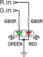
The overall status of the TikerNut can be determined at a glance by checking the bi-color status LED. This is connected to the microcontroller pins PE6 and PE7 through two current limiting resistors.
![]()
The pins are energised using pulse width modulation allowing the brightness and color of the status LED to be easily set from green through orange to red.
In normal operation the LED presents a pulsing heartbeat to show the system is alive. The pulses are green to indicate good health while other colors indicate problem states. Current status reports have LAN connectivity issues pulsing orange and radio connectivity issues pulsing red. The LED also briefly blinks red on infrared remote reception and blinks yellow during SD card access.
Network status LEDs:
The three original network status LEDs proved quite handy, showing link status and network activity. Originally they were mounted directly on the network module and would have been obscured within the case.
![]()
To make the LEDs visible they have been repositioned to the front panel and the status signals have been routed from the network module to the control board.
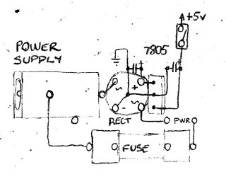
Power supply:
The internal power supply produces and regulates the main 5 volt rail which supplies power to all of the components throughout the system.
![]()
The input to the supply is designed to suit a wide range of low voltage adapters and it can use either AC or DC between 7 and 15 volts with at least 500 milliamps.
A supply fuse is mounted on the motherboard to protect against possible fire hazards. It is first to receive the supply voltage after it returns from the front panel power switch. A bridge rectifier then sorts out supply polarities and connects negative to ground. Supply positive is fed via a reservoir capacitor to a 7805 linear regulator on a small heatsink. The output of the regulator connects via another reservoir capacitor through the supply isolating jumper before feeding the main 5 volt rail.
Additional to the original design is the addition of an LM35 temperature sensor to monitor the heatsink and voltage dividers to monitor voltages before and after the 7805 regulator. These monitors feed their analog outputs to ADC inputs 0, 1 and 2 on the CPU and are sampled a few times a second to check for out-of-range conditions and can shut down the Tickernut to try and prevent damage. I felt this could prove wise given the brutally hot summers we have been having in Australia.
![]()
-
4Step 4
Tickernut firmware:
![]()
Ethernut is an Open Source Hardware and Software Project for building tiny Embedded Ethernet Devices. It consists of a set of hardware designs all running an open source operating system called Nut/OS and a TCP/IP protocol suite named Nut/Net.
Ethernut has a comprehensive range of excellent quality instructions and comes with a superb set of examples. It is well supported and sustains a thriving community of users on the informative NutWiki.
Nut/OS operating system:
Nut/OS is a capable, low-spec RTOS with a highly configurable modular architecture and support for a wide range of hardware. It provides priority driven cooperative multitasking, dynamic memory management and a range of timers. In order to remain simple Nut/OS contains only the minimum amount of services required by the EtherNut TCP/IP stack.
Thanks to a clever modular architecture the compiled firmware contains only needed library routines. The libraries provide a C stdio API and drivers ready for a large number of devices.
Nut/Net TCP/IP stack:
Nut/OS contains a powerful TCP/IP stack. Along with basic TCP and UDP sockets several high level protocols are available like DHCP, DNS, FTP, HTTP, SMTP, SNMP, SNTP, syslog and others. These are being used to very good effect in the Tickernut.
Nut/OS on the Tickernut:
Configuration of the Nut/OS source code is handled through the Configurator, a marvellous GUI interface. This tool also manages the board profiles and comes with a vast collection of profiles covering many hardware variants. Using this tool, one sets up an appropriate hardware configuration, builds the libraries and prepares the application's build environment with style and ease.
With the libraries configured and built for the Ethernut 1.3G reference design the Nut/OS examples ran on the TickerNut hardware out of the box. The Ethernut 1.3G profile was used as a starting point to construct a more customized Tickernut profile.
TFTP Bootloader:
At a very early stage the newly completed Tickernut appeared fully functional and appeared to be trying to struggle free of it's programming tether, although that could have been me tripping over all those wires. In order to allow development to continue safely it was decided a LAN bootloader was the first order of business.
Ethernut is provided with the excellent Netboot TFTP bootloader. Once the TFTP server was in place on the network the bootloader worked flawlessly. In fact the very first update flashed over so quickly I missed it completely and thought it had not worked at all.
A closer look at Netboot revealed enough space left over in the bootblock to allow the bootloader to be customised to better suit the Tickernut hardware. A simple stand-alone LCD driver was grafted in to allow Netboot to use the LCD display to report status and progress. Status LED control was also added to allow Netboot to clearly indicate its progress or failure.
LCD display driver:
The LCD display was absurdly easy to integrate into the system using the generic HD447800 driver provided by Nut/OS. The hardware configuration of the display connections was chosen match the default setup in the Configurator so the Nut/OS libraries were ready to go.
In the application, after a simple call to NutRegisterDevice, the LCD display can be opened and written to and behaves as a terminal emulator. The driver interprets escape codes for formatting and access to the HD447800's special functions.
Audio driver:
The first version of the sample player played short bursts of sound from uncompressed raw audio samples embedded in the flash. Later versions retrieve sample data from WAV files on the SD card.
Audio is produced using the Output Compare signal from timer 2 to generate a pulse width modulated waveform. The timer is clocked at the sample rate of 11.025Khz and a new sample is loaded into the timer's compare register every cycle. The sample rate is high enough that the audio does not require additional low-pass filtering.
Infrared remote decoder:
I was not able to get the Phillips RC5 protocol decoder included with Nut/OS to work for me. This is most likely because glitches and noise in the IR signal line were causing total havoc with timing but evaded detection until after a new decoder was implemented.
The decoder for the remote control codes recognises the common NEC protocol and is implemented within an interrupt service routine. This routine is activated by an external interrupt triggered from the negative going transitions of the remote's message.
The time between each interrupt is measured by timer 3 and is used to determine the current bit value in the serial data stream. The signal glitches were characterized by very short bit times and once discovered, were easily rejected. The bits are shifted into a message buffer and the thread listening for remote control commands is notified once a complete message becomes available.
Telnet configuration interface:
The first server written for the Tickernut was a simple telnet command line interface with a limited set of control functions. These have been expanded to allow querying and setting basic network parameters, bootloader TFTP parameters and triggering the bootloader as well as querying current memory, timer and thread usages.
The telnet interface is used by my in-house NutBoot firmware manager to set the TFTP parameters and trigger the bootloader to perform remote firmware updates on the Tickernut. NutBoot provides easy glossy buttons to perform common Tickernut actions like ping test, remote reset and a bootload launcher along with a simple terminal. NutBoot can also monitor a binary firmware image and flash it automatically when it is updated.
nRF24L01+ driver:
The nRF24L01+ radio modules communicate as master and slave. The Tickernut sends packets as required to which the Lexitron always responds immediately with either an ACK or data. If the Tickernut does not receive a response in good time, it sends the packet again.
Now packets are tagged with a sequence number that is incremented for each new packet. If the Lexitron missed the first packet it will respond as normal to the second packet and everything is all right. If instead it had replied to the packet and the Tickernut had missed the reply, the Lexitron will see the sequence number of the previous packet is the same as this one. In this case the Lexitron replies but does not act on the content of the packet as any actions or commands would already have been performed.
This provides a robust, persistent link layer for the higher-level Lexicom driver.
Lexicom protocol:
nRF24L01+ packets are 32 bytes long. After adding the sequence number, the link layer provides 31 byte packets. All Lexitron commands are 31 bytes long or less. Commands are buffered by the Lexitron and may take long times to execute so the first step of a communication is querying the Lexitron's status and reading the flags to check if the buffer is full. Once there is space in the buffer, the packet is sent and a reply sought.
Many commands chain together, so a series of scroll commands can scroll on long messages without pause between sections. The buffer is large enough to hold several seconds of activity, allowing the Tickernut to move on and start preparing the next message while the current message is still displaying on the Lexitron.
The command set currently includes basic text and bit-mapped graphics, simple icons and a small selection of display modes, movements and fonts. Integrated into the command set is a bootloader interface that allows the Lexitron to self-program over the radio from from the NutBoot firmware manager through the Tickernut.
Status LED:
The status led is driven by two pulse width modulated signals from a pair of left over pins on the microcontroller. A high speed timer interrupt increments a register to produce a ramping value. The interrupt then uses comparisons between the ramp value and the desired brightnesses to toggle the respective status LED's output pin producing a PWM signal that can steadily and smoothly vary the brightness of each colour independently.
A thread is devoted to controlling the brightness of the status LED. This lowest priority loop works in the background to ramp the brightness of the status LED up and down in a pulsating rhythm as well as providing the stopwatch for timed indicator blinks. As a steady pulasting heartbeat requires the operating system to be mostly alive and responsive, the lack of one is a sure indicator of a critical fault or catastrophic crash.
Applications can set the colour of the heartbeat and can also request a steady colour for a specified period. For example, when the thread waiting for infrared recieves a new command it sets the status LED a steady bright red for a short period to provide the remote control confirmation blinks.
![]()
-
5Step 5
Tickernut construction log:
![]()
Construction was completed in stages over the period of many months with a design that evolved to suit the available parts. The progression of construction was arranged so that each stage could be completed and tested before moving to the next stage.
Case:
Construction began with the case. I seem to get better results starting with the enclosure. The very first step was going through the shed to find a suitable box. The best choice appeared to be an old telephone exchange hold music adapter in a jiffy box that had almost no existing holes.
The design of the TickerNut is heavily influenced by the choice of enclosure. It was a challenge and quite risky making this kind of construction fit a small case. A larger case would have made the build much simpler. Despite this I was able to weave all the components around each other in the right order and more by luck than good planning everything fit neatly.
The final build is densely packed with little wasted space but is still easily accessible and disassembles and reassembles quickly for servicing. The front panel has a single cable connection to the body which is long enough to operate the unit safely with the lid off.
The only devices that are attached to the case are the tiny speaker in it's grill and the antenna off an old cordless phone. All the other connectors, controls and indicators are mounted on the circuit boards and protrude or are visible through cutouts in the body and front panel.
![]()
After gathering a set of switches and LEDs from an old photo developer and an LCD out of the junk box I began by arranging them on the front panel. Once a layout was decided the panel was drilled and cut out and the windows were fitted.
![]()
The body of the case was drilled to accept the speaker and the antenna. A motherboard was cut from a sheet of prototyping spot board and provided with mounting posts in the bottom of the case. Plugs were positioned on the motherboard and the case wall was cut out to expose the connections with the motherboard in place.
![]()
The case was then painted with charcoal hammer finish spray paint and left for a week or so to cure. The speaker grill was originally off a toy dog and had been chopped and shaped to fit so it was also painted to restore it's finish.
![]()
A veroboard backing was arranged to hold all the controls in place behind the front panel with the threaded collars of the two reinforced PCB-mount switches protruding through the panel to provide a simple, strong mounting.
![]()
The infrared remote control reciever was added as an afterthought as I had forgotten to include it during the initial panel build. It is mounted on a little outrigger soldered off the control board so it can see through a tinted window in the top of the front panel.
![]()
The basic enclosure was now complete and ready to go. At this stage the motherboard only contained devices which protruded through the case, namely the power socket, programming plug, serial port and the headers for mounting the network module.
Processor module:
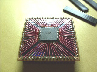
The next order of business was making the surface mount microcontroller available to the rest of the circuitry. I wanted to try a low-tech, hands on method of breaking out the tiny pins on the chip to more manageable dimensions. I know ready-made breakout boards come cheap but I didn't have any and I decided was going to approach this challenge using only the junkpile.
![]()
I wanted something that was removable for repair and upgrades, so sockets and pins were part of the original concept.
![]()
I cut a scrap of prototyping spot board just big enough to allow four 16-pin headers to fit along it's edges and soldered them in place. The unused portion of the top of the board was covered with black adhesive film to enhance appearance. The microcontroller was mounted in the center of this board with a small square of double sided foam tape and it's pins wired to the headers to make a quick and dirty breakout board.
![]()
By quick, I mean it took me about two hours to complete all four sides. Despite the tiny solder joins the assembly is relatively sturdy and coped well with being handled, only needing three repairs due to rough treatment over it's service life. The wire used was recovered from a web of wire-wrap on the back of a rack of very old industrial controller cards. This wire is solid core, very fine and too stiff to be copper, I think it's silver. The insulation is confoundedly strong and does not shrink back when heated allowing neat solder joins.
![]()
The four rows of header pins around the edge of the processor module fit into sockets intended for the motherboard. The network module was already in position with the remaining unused area on the motherboard looking like half what I felt I needed.
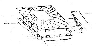
Alternative layout:
![]()
I considered this layout but discarded it as it would have been too cramped.
Memory module:
![]()
It soon became clear the memory chips did not want to fit directly on the motherboard so I set about constructing an outboard memory module that would provide decoded bus signals ready for the network module to use. I knew a lot of pins would be required so I began with a large 40 pin right angle connector.
![]()
The circuit needed to occupy the smallest amount of space and a couple of ribbons of links were tolerated in the design. The finished memory module when installed clears the inside of the lid by millimeters.
![]()
This allowed the layout of the motherboard to become much more reasonable. The memory and processor modules were hugged up as close as I could manage against the network module and as far away from the connectors as possible. This left a small strip of free board along the top and down one side, perhaps it could prove enough for the remaining components.
![]()
Motherboard:
![]()
The space on the motherboard was severely limited requiring circuits to be very dense and tightly packed. Several component layouts were considered and discarded. Circuit boards needed to be layered over other circuits to minimize space requirements. Once I had estimated the positions of the major components I could begin the wiring process.
The first functional part to be placed on the board was the processor socket. After soldering it in I added the memory socket as a placeholder.
![]()
I then wired as many support components within the processor socket as I could. System crystal, real time clock crystal, reset monitor, analog supply and decoupling capacitors were installed along with the beginnings of the power distribution network.
![]()
Serial Port:
![]()
The serial port was the first general purpose peripheral to be wired up. The MAX232 line driver chip requires a bunch of energy storage capacitors for the internal DC-DC converter. The datasheet specifies 1uF and many applications use 10uF although I have seen 100nF successfully used in some devices. In order to make the circuit physically small I took a chance with tiny 100nF chip capacitors. These have worked perfectly well.
![]()
The MAX232 chip was positioned beside the processor as close to the RS232 plug as possible. Signals from the plug were routed to the chip under the board and the converter capacitors were installed. The supply rail was extended to include the MAX232 and stakes were installed for processor connections.
![]()
Power supply:
![]()
The time had come to give the Tickernut it's own power supply. Components in power supplies tend to be large and I only had a limited amount of space beneath the network module. Despite this I wanted something with a universal input and protection against inevitable mistakes.
![]()
The regulator heatsink was bent and shaped for a flat profile. The largest electrolytic capacitors I had that could be made to fit were employed. A bridge rectifier and fuse were also fitted. The external power pack initially chosen for the Tickernut is a Telstra branded 9 volt 500 milliamp wall wart that once charged the same cordless phone the antenna was sourced from.
![]()
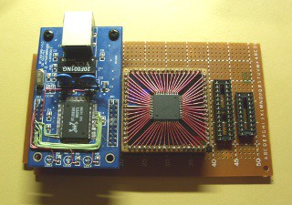
Radio modem:
The first set of radio modules were installed in the small strip of free space left over at the very top of the motherboard. They are placed close together with the antenna connections adjacent to one another and the common antenna connection stake wired between both. The data signals from radio modules are simply wired straight to the second UART on the processor.
![]()
The transmitter module proved too large for it's position and fouled the back of the control board when the front panel was placed on. Peeking through the gap in the lid it seemed the module was catching the edge of the control board. Another transmitter module I used to template construction was smaller and fit without problem but I had earlier decided to swap over as it appeared to be on a different frequency.
![]()
I bent the pins of the transmitter so it leaned toward the wall of the case. This allowed it to clear the control board and let the front panel fit cleanly and is why the transmitter module sits at such a rakish angle. A fixed cable was run to a connector that mated to the spade lug on the antenna base.
Network module glue logic:
![]()
A 74hc00 was installed in the area under the network module to provide inverters for A15 address decoding and to correct the sense of the interrupt and reset signals to suit the NIC.
![]()
Later modifications have altered this area to rearrange the address map and make more memory available.
![]()
The new memory map moves the RTL8019 registers from 0x8300 to 0xC300 to allow previously inaccessible ram to be mapped into the area 0x8000 to 0xA000.
![]()
This is providing an extra 8K of physical ram by simply rewiring the 74HC00 and reconfiguring Nut/OS.
Memory installation:
The memory module socket was already installed and a bunch of board connections had been soldered in place during the processor installation but there was more to go before the memory would work.
![]()
A tangle of links to sort out the high order address lines were tucked in between the processor and memory sockets and the modules were plugged in.
![]()
Initial testing:
![]()
Running power distribution around the board let me introduce the ISP programming plug to the system. With that on the supply rails I had an opportunity to check my work. I ran a set of temporary wires to bring the processor's programming signals to the ISP port and set the jumper that connects the programmer to the supply rail. I then went over it all again before powering up the processor for the first time.
There was nothing. I examined all the connections and repeated all the voltage and continuity tests but could find nothing amiss. I even dragged out the datasheets and went over the design again. I suspected my home-made AVRISP programmer but it was working fine on other projects. Out of desperation I dug up my old AVR910 serial programmer and an external power supply. Hardly expecting anything I powered up and hit the button.
It came as quite a shock when I realized the processor suspended in it's spider web of wires was alive and responding to the programmer. The fuses of course were all still set to default and the system clock was using the slow internal source. It appears my AVRISP programmer's old firmware was streaming the data over too fast for this mode.
I altered the fuses to use the external crystal and untangled the board from the temporary supply. Plugging the powered AVRISP programmer back in I found the processor ready and waiting. It was time to give it something to do.
Serial:
I checked the circuit and applied power. Finding a healthy +12 and -12 volts coming out of the DC-DC converter let me know the MAX232 chip was powering up. At this stage I had prepared the EtherNut diagnostics firmware and already flashed it to the processor. I wired the TxD and RxD signal lines to the serial port and fired up.
My serial terminal responded with a blurt of garble. More garble followed and it looked like the Tickernut was trying very hard to speak it's first words despite the difficulty. Tinkering with serial settings did not help.
In the initial build I had substituted a 16Mhz crystal for the system clock. The Ethernut reference design uses a 14.7456Mhz serial speed crystal which I had found difficult to obtain. The plan had been to tune NutOS to cope but I had not yet got that far. Rummaging through my scrap produced a 14.31818Mhz crystal as the closest speed I had. According to some sources a 3% serial speed error is tolerable.
Replacing the crystal produced a page of clear text from the diagnostic program informing me everything was fine despite the fact it failed to initialize either the RAM or the NIC. It was also presenting LAN configuration options.
I soon discovered that in the process of installing the serial hardware the ISP programmer had stopped working. The serial lines are shared between the two modules and the MAX232 chip was holding RxD high. A resistor was added on the MAX232 RxD signal to allow the programmer to take control of the line. This brought the programming port back online and as a bonus the serial port still works even with the programmer connected.
SRAM:
After sorting out an omitted power connection to the socket the diagnostics reported 32K of useable RAM had become available. It passed pattern testing without trouble showing the bus was correctly wired.
PSU:
The power supply came together without a hitch but the small filter capacitors leave it with very little power in reserve. Even a short glitch in the mains supply causes the Tickernut to brown out and reset.
The demand on the power supply is moderate and the small heatsink on the regulator gets quite warm. Later improvements to the power supply included an extra large filter capacitor and heatsink temperature monitoring.
Network Module:
The network module as purchased only provided the low five address lines on the connector. This is enough to access the RTL8019's 32 control registers but the EtherNut design takes advantage of the fact the RTL8019 NIC can decode a whole address bus and uses all 16 address lines provided by the NIC chip.
Emulating this requirement using the five available lines would have required external address decoding hardware. The simplest of this would have repeated the NIC registers over and over every 32 bytes throughout the memory space above the RAM. This would have worked but makes adding more peripherals to the bus in the future a difficult proposition.
In the end I decided to modify the network module itself in order to provide a clean memory map without needing extra hardware. I had already planned to alter the module to bring the status LEDs out the front panel but this was a much more difficult proposition.
The pins on the RTL8019 surface mount chip are even finer a pitch than on the processor. The pads I wanted to solder to were mostly sequentially positioned and were already connected to power and ground to hardwire the high order address.
The first job was to chisel away these connections to isolate the solder pads holding the address pins. This was followed by a forest of fine wires carefully soldered to each of the pins. These were folded into a bundle and routed around to the spare connectors on the socket. The bundle was cemented in place with a couple of drops of super glue in the corners.
More wires were added to reroute the status LEDs and the reset signal. More super glue was added to ensure the wires were firmly anchored in place. The network module was now good to go but the motherboard was not ready for it.
The network module requires a lot of connections to the rest of the system and all but three were made to the module headers by flying leads between solder posts. This was the start of the large bundles of flying leads routing all over the top of the motherboard.
To keep the leads neat and firm I intended to lace them together into a loom. Each lead was roughly measured before being cut, tinned and soldered.
With everything in place I did a double check and fired up. The NutOS diagnostics firmware failed the NIC test although the Netboot bootloader appeared to be able to initialize it without complaint. The memory module had also suddenly failed indicating a short on one of the bus lines was the likely fault. A scan of the memory map with the RAM chip out of its socket revealed the RTL8019's registers being repeated every 64 bytes. This told me to check address line A5 on the demultiplexed bus.
Sure enough a short was detected and was traced to the NIC module itself. It turned out the A5 pin on the RTL8019 chip was being grounded via a connection under the chip that I had missed when I had first tried to isolate the solder pads. Unable to get at the track, I lifted the pin off the board and soldered it's connection floating. I was not happy with this arrangement so I reinforced it by sticking slivers of adhesive paper label above and below the pin to insulate it then varnished it with super glue to provide protection.
All the butcher work on the network module had finally provided results. The module powered up, the diagnostics passed the NIC in all tests and it appeared to be functioning correctly. Sure enough it happily responded to being pinged. The diagnostic program had also suddenly sprouted extra options including starting a mini web server. This kicked over without complaint and the Ethernut logo shone back at me from a browser window.
Audio amplifier:
The audio amplifier was based on the LM386 which is a tiny 8 pin chip that needed to fit in the smallest possible patch of board. The simplest circuit that could produce sound from this chip was tucked in around it's socket and enough space was found to include a tiny trimpot for the volume control.
The power supply for the amplifier needed to be heavily decoupled as the main 5 volt rail proved far too noisy to drive an amplifier directly. When I initially powered up the amplifier the unit produced loud constant buzzes and squeals that were synchronised to the processor's operation. Interesting as a kind of circuit stethoscope perhaps but not quite what I was after. The sound could not be affected by the volume control which is a common symptom of supply induced noise.
The simple solution was to isolate the amplifier supply behind a 4.7 ohm decoupling resistor and give it a large tantalum reservoir capacitor. This effectively supresses supply noise to a soft whisper but it restricts the amount of sustained power available to the amplifier. This limits maximum volume and increases distortion on loud passages but this is barely noticable through the tiny speaker.
During the initial stages of radio modem testing another issue with the amplifier was discovered. The unshielded nature of the TickerNut's construction and wiring with the proximity of the RF modules to the sensitive audio stages caused a loud burping to be emitted from the speaker during radio transmission.
The crowbar solution for this was to simply install a low-dropout mosfet switch on the audio amplifier's power supply so as to only turn the amplifier on during sample playing and have it off during radio transmission. This may seem a brutal approach where shielding would perhaps be considered the proper solution but this method has been used in CB radio designs for years.
This has turned out to be completely effective with the advantages of total silence and reduced power consumption when the amplifier is quiet and the minor limitation of not being able to produce sound and transmit at the same time.
More recent revisions of the audio driver and the upgrade to 2.4Ghz radio modules has now eliminated this shortcoming.
Front panel installation:
The cable connecting the front panel to the motherboard was the last item to be constructed and presented quite a challenge. The sockets on the back of the control board were already installed and ready but there was no space left on the motherboard for the required sockets at the other end.
I briefly considered permanently wiring the cable into the loom and only having plugs at one end but this felt like a defeat so I persisted. I finally decided to drill a new set of holes in the edge of the motherboard to mount the sockets and reshape some useless solder pads beneath to hold them and a set of stakes in place. The result is somewhat untidy but strong and firm and faithful to the Tickernut's design. With the loom finished and laced up the motherboard was now ready to go.
The cable itself was formed from two strips of ribbon which were shaped and held in place together and reinforced with bands of heatshrink. When inside the case with the front panel on the cable tucks neatly into a recess beside the memory and network modules but when the front panel comes off it is long enough to hold the control board well out of the way and still see the display while poking around inside the case.
I originally used a really old LCD display module with an electroluminescent backlight and negative contrast voltage. It initially worked well but after a week of operation dead black horizontal lines appeared overlaying the normal text. Other groups of pixels were greying out showing a definite fault in the display as they are not normally capable of producing greyscale.
The LCD display was desoldered for a closer look and small spots of heavy corrosion on pins and connectors told the story. This display appeared to have been subject to a rodent infestation some time in the distant past. It was surprising it had worked as well as it did.
A replacement LCD display was sourced from an fancy old computer monitor and had a compatible footprint and connector. A pitfall was avoided when I noticed the display's expected ground pin did not have continuity to it's metal frame. It turned out the power connections on this display are the reverse of the old display while all other signals remain the same. Traps for the unwary I suppose.
the new display's LED backlight allowed me to dispose of the EL inverter running the old backlight. I switched the supply lines and rewired the contrast control for positive voltage and the new display cranked up first time. My dissappointment at the first module's sneaky failure was eased by the fact the new display is brighter and the contrast is much sharper.
Completed:
This completed the initial build stage of the Tickernut with all hardware functional and ready. I was pleased with the result, but as a working device it was still unfinished. Developing the application software would take much more time, and would highlight the limitations of the system as initially designed. More memory was needed, both RAM and flash, better radios and an SD card.
![]()
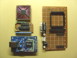
Lexitron RSS Reader
A self contained remote display system provides notification and display of feeds, weather reports, email, messages and of course, a clock.


Discussions
Become a Hackaday.io Member
Create an account to leave a comment. Already have an account? Log In.