 Marc-André Denis
During the flight of a sounding rocket, it is not possible to keep an antenna pointed at the sky at all time. Since the electronic bay is located inside the nosecone, the antenna is facing the sky during the ascension but face the ground after the parachute deploys. The use of the traditional ceramic patch antenna is not ideal since the are directional.
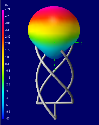
The quadrifilar helix antenna is used since it is a less directional circularly polarized antenna.
Antenna frequency
The antenna is designed for the following bands:
GPS L1 : 1575.42 MHz
GLONASS L1 : 1598.0625-1609.3125 MHz
Galileo E1 1575.42 MHz
SBAS L1 : 1575.42 MHz
Design of the antenna
Since there are no exact formulas for designing this type of antenna, a numerical modelling approach is used. The NECPP python library is used for the optimisation of the antenna geometry and the 4nec2 software is used for the validation.
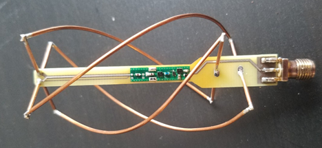
The antenna is composed of 2 loops of around one wavelength in length that are rotated. To achieve the circular polarisation, there must be a phase difference of 90˚ between the tow loops. One of the loops is made smaller and the other larger so they have an opposite reactance.
The following parameters are used as a starting point:
Length of one loop: One wavelength in air -> 190mm
Diameter of the antenna: 30mm
Number of turns: 0.5
The scypy library is used to optimize the antenna geometry for the highest circularly polarized gain.
The script is available here: https://github.com/le-Bark/QFH-Antenna
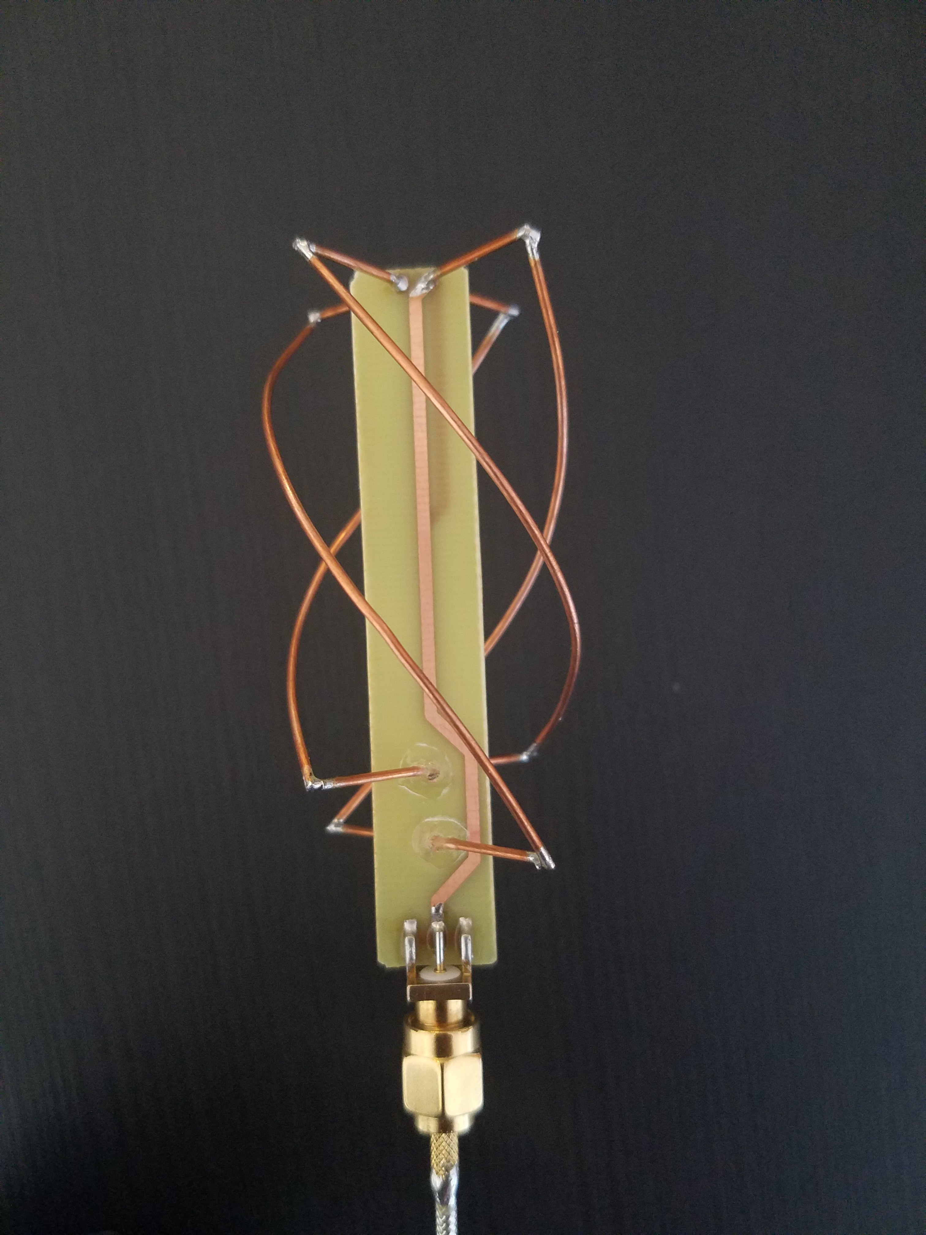
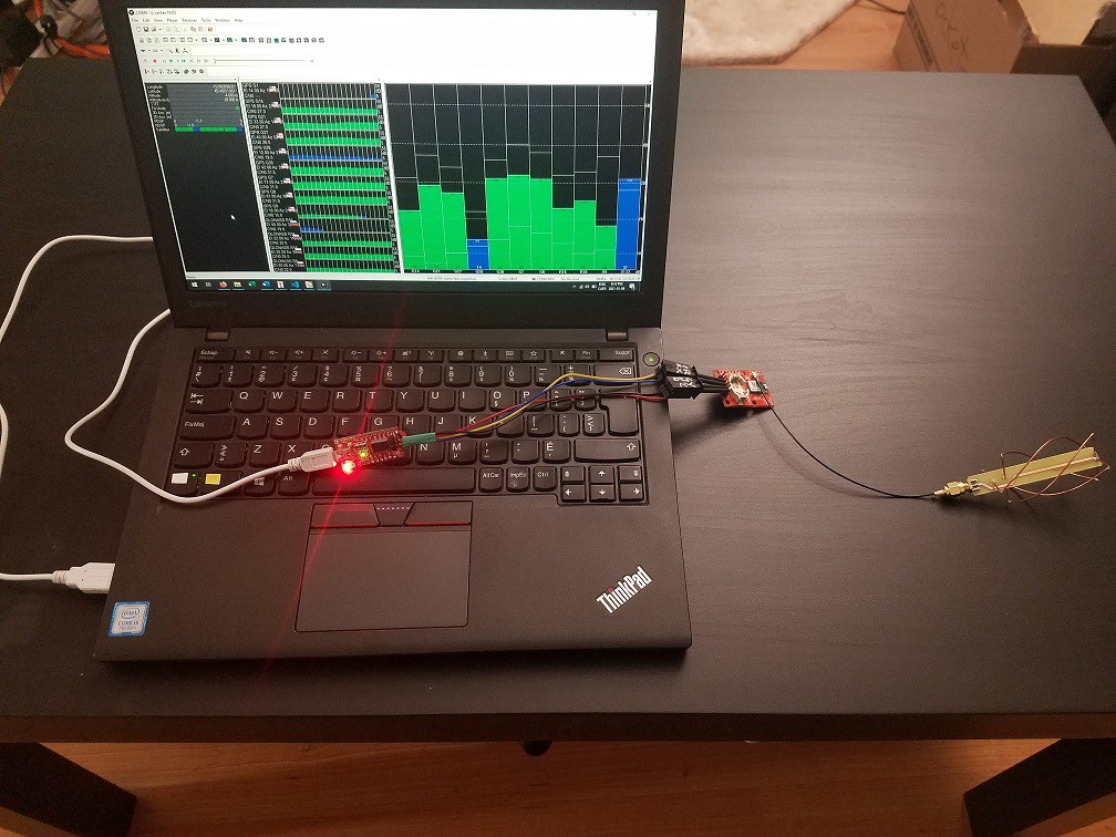
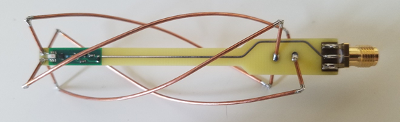
The first prototype of the antenna is built using a PCB as a support. The PCB contains a quarter wave folded balun, a 50 ohm micro-strip and a SMA connector.
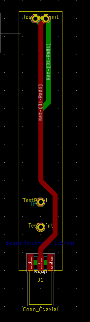
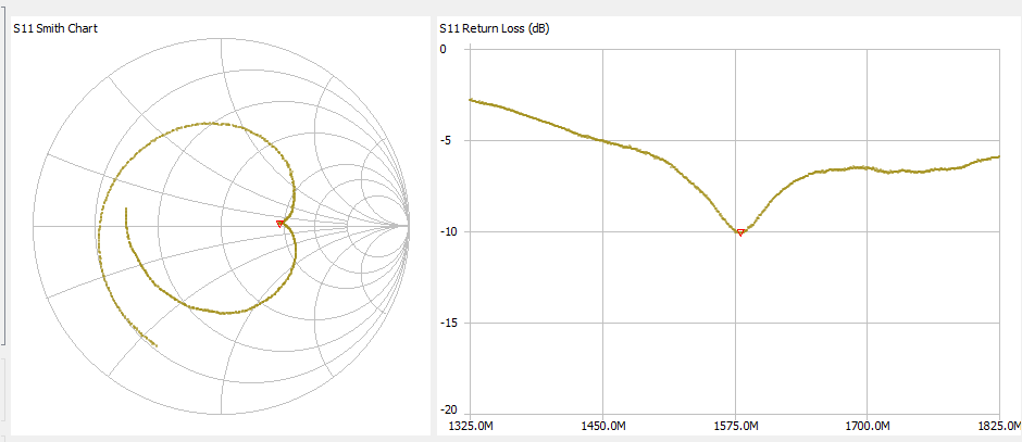
The antenna is measured using a NanoVNA, the frequency response is as expected. The impedance of the antenna is 95+J2 ohm and will need to be matched on the next prototype.
The unmatched Antenna is then tested successfully using a U-Blox GPS module.
Active antenna
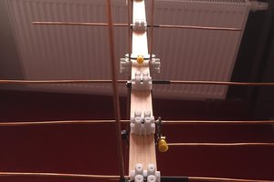
The design is based on the BGA524N6 LNA IC from Infineon. The LNA circuit is placed in the middle of the antenna on the support PCB.
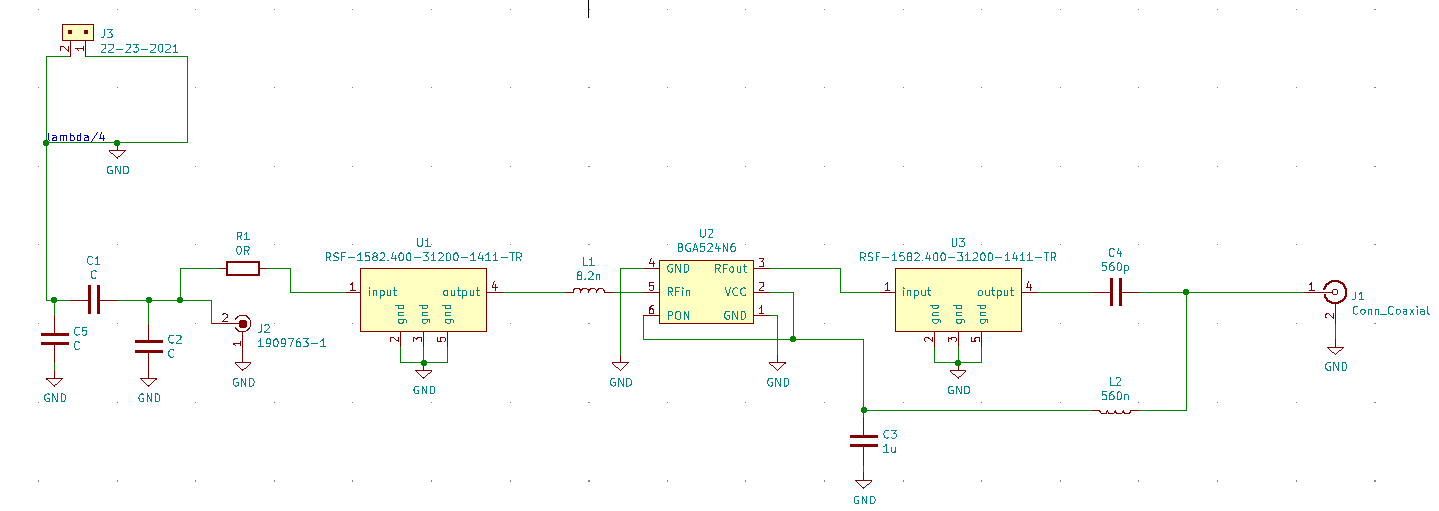
The PCB is a 4 layers controlled impedance board from JLC PCB.
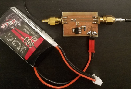
The antenna is assembled and tested using a similar setup. A bias tee is added to power the LNA.
There is a greater number of satellites with a higher signal strength.
One last version was made using a balun IC and a diameter of 25mm. The footprints for the matching network were also removed.
 A passive version was also made and sent to antennatestlab for analysis. The results are consistent with the simulation except for an asymmetry in the radiation pattern caused by the transmission line.
 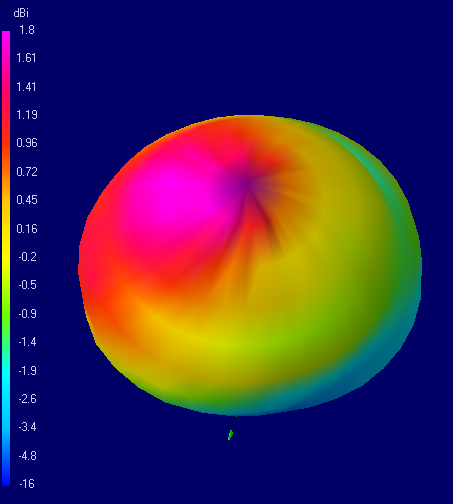 The results are available in the attached files.
 Thanks to Glen Robb at Antennatestlab for making the tests possible.


 Elia
Elia
 ElectroBoy
 ThunderSqueak
 Ahmed Hefnawi (Volta)
What is the purpose of having the PCB feed traces going thru the middle when you can have the spiral elements running above and after the matching network ? It seems like you are making this harder than it needs to be. The elements are going to couple with the microstrip and may form other oscillatory coupling problems. It would seem like the most elegant solution is the run immediately into the BPF-NLA-BPF as quickly (shortest) as possible, then the matching network, and then right into the feed point. The element recombination point would be at the top end of the antenna. Also since this is basically a twisted folded dipole, each side needs to be the same length to be balanced. The problem occurs at the cross over. I would recommend a small half-arc upward for one and a small half-arc downward for the other. Bear in mind that there will be capacitive coupling in this area and adjust your arcs to minimize this.