Wenting Zhang
-
What happened to this project?
11/20/2021 at 14:11 • 0 commentsI haven't provided any update about this project for a very long time, so what happened?
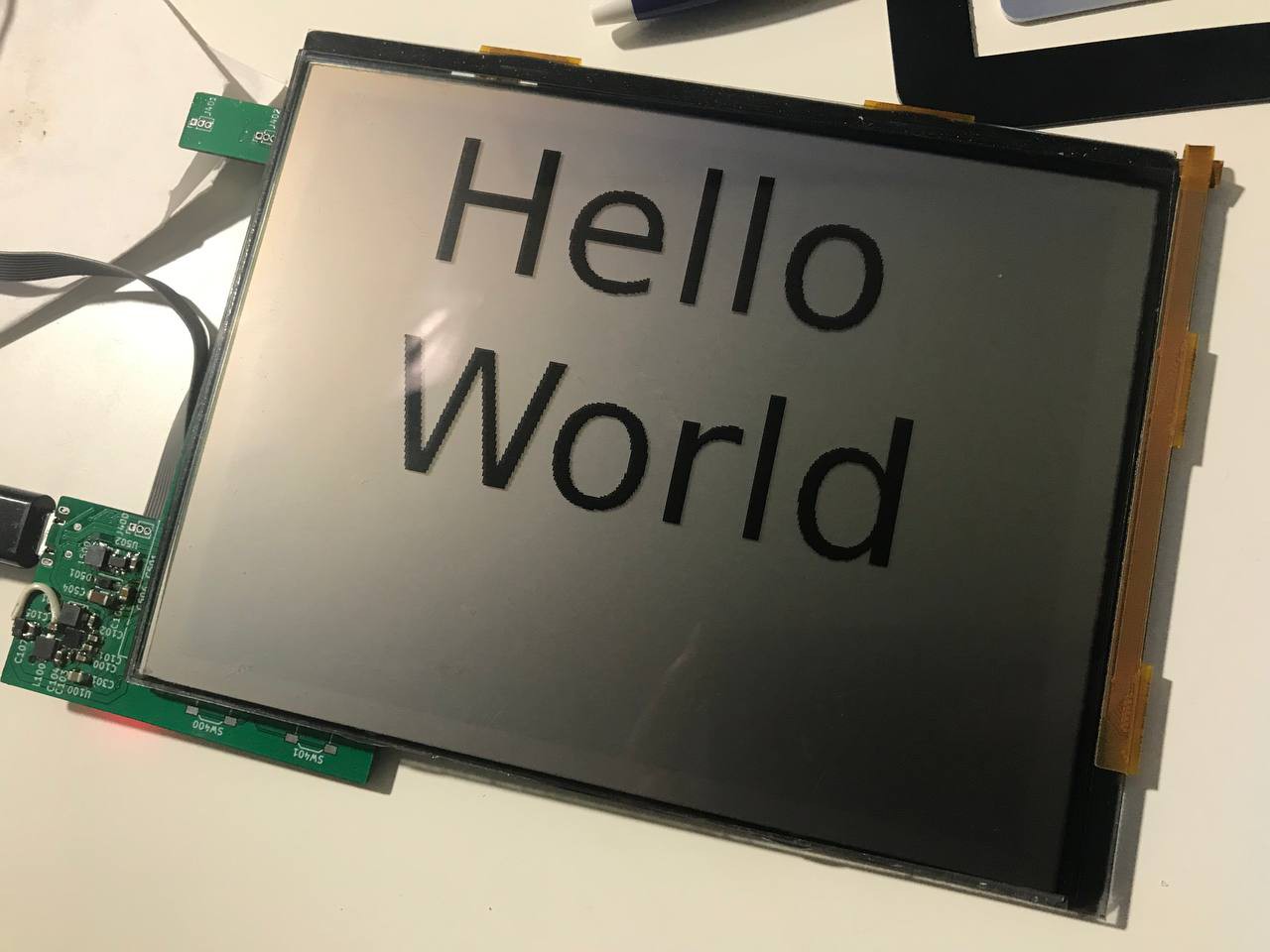
In the last update I mentioned the R0.1 PCB was alive. It worked well and I played with it to test several ideas. The real issue of making it into a eReader is the screen update speed. It's being too slow to be used as an interactive device.
The full screen update takes ~3s (including erase time), this means each page turn takes that long time. Though UI interactions could be a bit better, if only updating 1/10 screen at a time (say like there is a menu on screen with 20 items, and moving one to the next one) it takes "only" 300ms. It could be workable but does not fit with my initial concept.
Well I know the screen is slow to begin with, shouldn't this be known from very early on? Sort of. I was trying to answer a question for myself: could the screen be refreshed like a normal volatile LCD? The original board was too slow for me to know, but with a much faster RP2040, I got my answer. The answer was detailed in the last update, but basically no. If that worked, it would be a quite cool and allow much more flexible UI design.
So what's next? This project has been cancelled. I am planning to revisit the idea of using a 6" reflective LCD to build something interesting in a later date. But for now, thanks for reading.
-
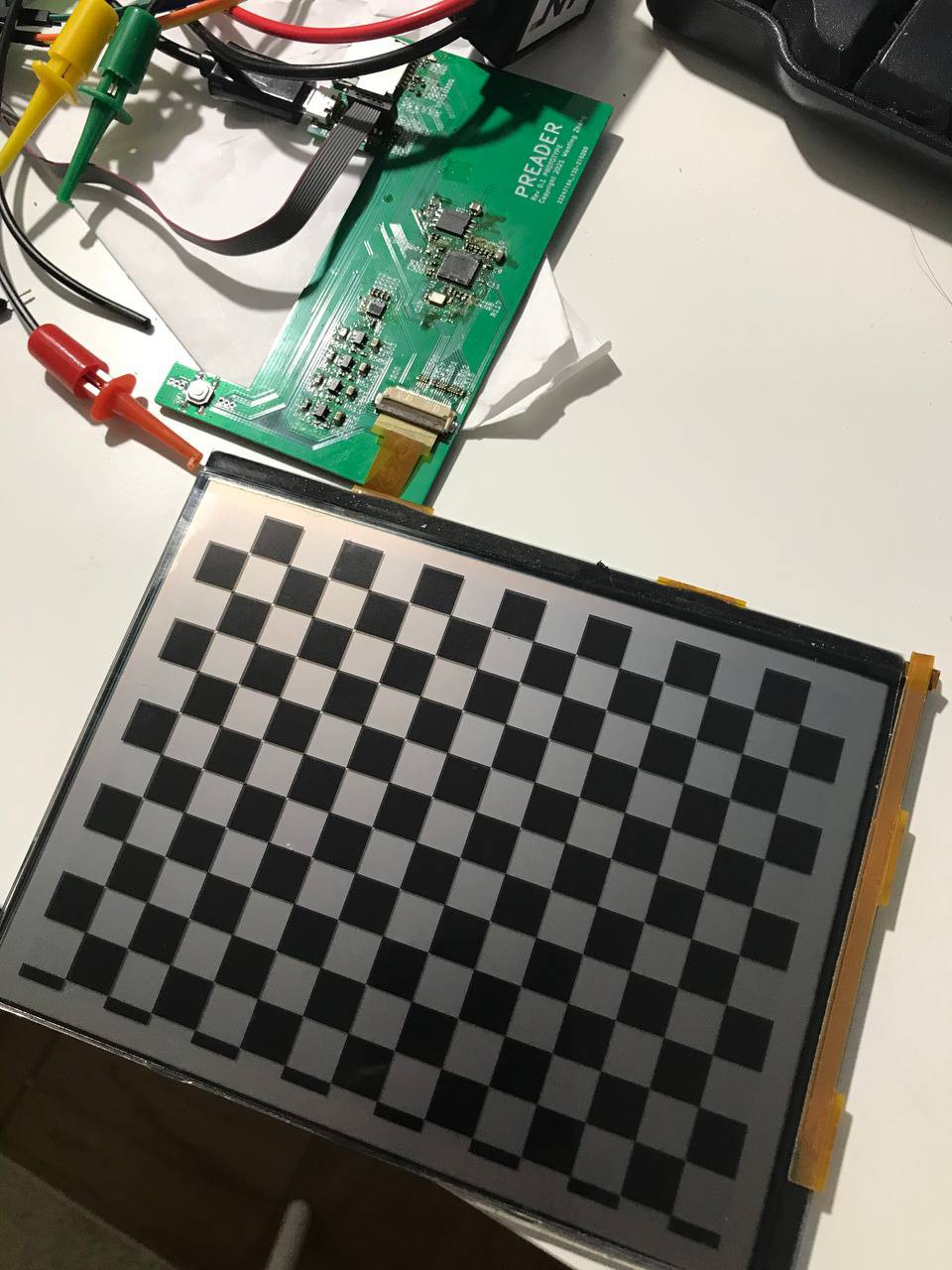
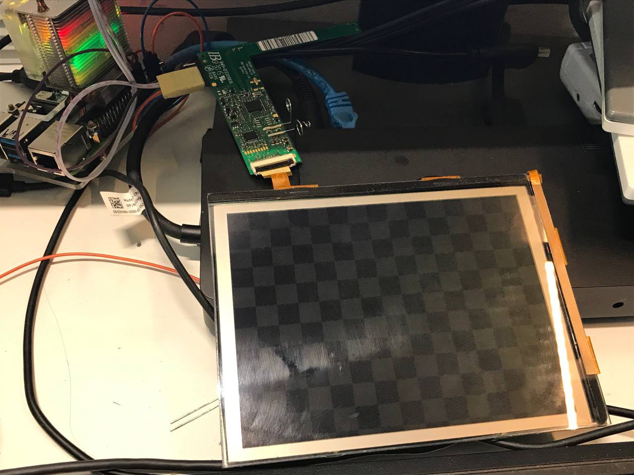
R0.1 PCB is alive
04/17/2021 at 12:54 • 0 commentsI know it has been a long time since I have finished the PCB design. I have finally had it soldered and working:
There aren't much to talk about right now, as the firmware is still mostly work in progress. The details about screen driving have been discussed in the previous log. But now with RP2040, It's possible to drive this screen at a refresh rate much higher than previously possible with CC1100.
This is a bistable LCD, and it takes ~1 sec to do a full screen update. But I would like to see, what if I don't need the image to be stable, but rather using it as a normal LCD? This first revision hardware also features a likely over-engineered bias generation circuit, to allow flexible bias generation to support high frame rate operation, if at all possible.
The answer is, yes, but actually no.
https://twitter.com/zephray_wenting/status/1382840220735971328
This is what it looks like when being driven at 30Hz, and the voltage is already at 32V. Driving it at higher refresh rate requires bumping up the voltage even higher, and will not improve the contrast ratio. This is the best contrast it could achieve when being driven like a normal LCD. So yes it could be, but the image quality is too poor to be used.
But what's happening here?
You've probably heard about different LCD technologies like TN, IPS, MVA for active matrix (TFT) LCDs. There are several different technologies for passive matrix LCDs as well: TN, HTN, STN, FSTN, and Double-layer STN (not to be confused with Dual-scan STN).
All passive matrix LCDs suffer from one issue: lines couldn't be driven individually. Think in an LED matrix scan situation, pixels in the active scan line are either forward-biased or zero-potential, and pixels in the non-active lines are either zero-potential or reverse-biased. But there is no reverse-bias in the LCD: they respond to the electric field, no matter its positive or negative. So all the unselected lines are being driven as well.
To deal with that, bias voltages and sophisticated driving waveform must be introduced. The goal is to make the RMS voltage on the active pixel higher than the RMS voltage on the inactive pixel (which is never zero, unfortunately). The contrast is then limited by two factors: the RMS voltage difference between active and inactive pixels, and how the LC responds to the voltage difference.
The first one is pretty much fixed value and can be calculated. The voltage difference decreases as the line count (vertical resolution) goes up. This means you are probably never going to see a very high resolution passive matrix LCD panel.
The second one could be improved by using different material and LC organization, which is doable but hard. TN only do well with resolutions under ~100 lines, and have poor viewing angle (20 deg or less). With STN technology and improved LC material, it is possible to scale up ~400 lines. With dual scan, which basically means putting 2 LC panels in one glass, the vertical resolution could scale up to ~800 lines. For this reason, there is basically no high-resolution TN passive matrix LCD. People had to use STN to get acceptable image quality.
So, what we are seeing here, is exactly a high resolution TN passive matrix LCD. It has extremely bad contrast ratio, just as expected. Yes though I expected that, but I still did it, just to see how bad it is.
Note when driving them in the bistable scheme, the screen only needs to drive one line into the stable state, then move on to the next line. The rms value on the inactive lines only needs to be low enough so they are not being driven into stable state, instead of low-enough to be invisible. In this case, the contrast ratio limitation no longer applies. The end result is an extremely high contrast image, that is very unlikely to be seen on other high-res passive matrix screens:
-
First prototype WIP
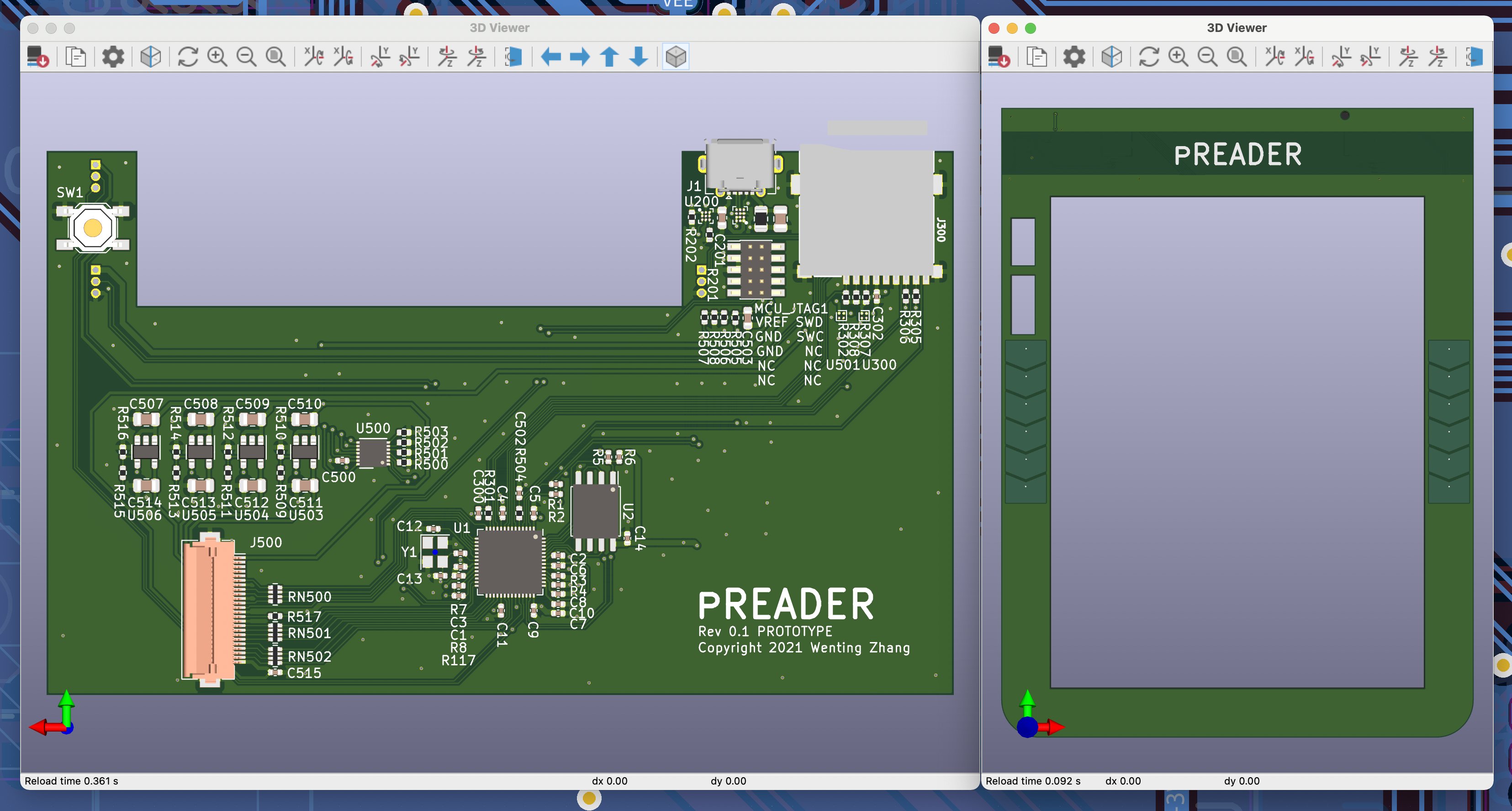
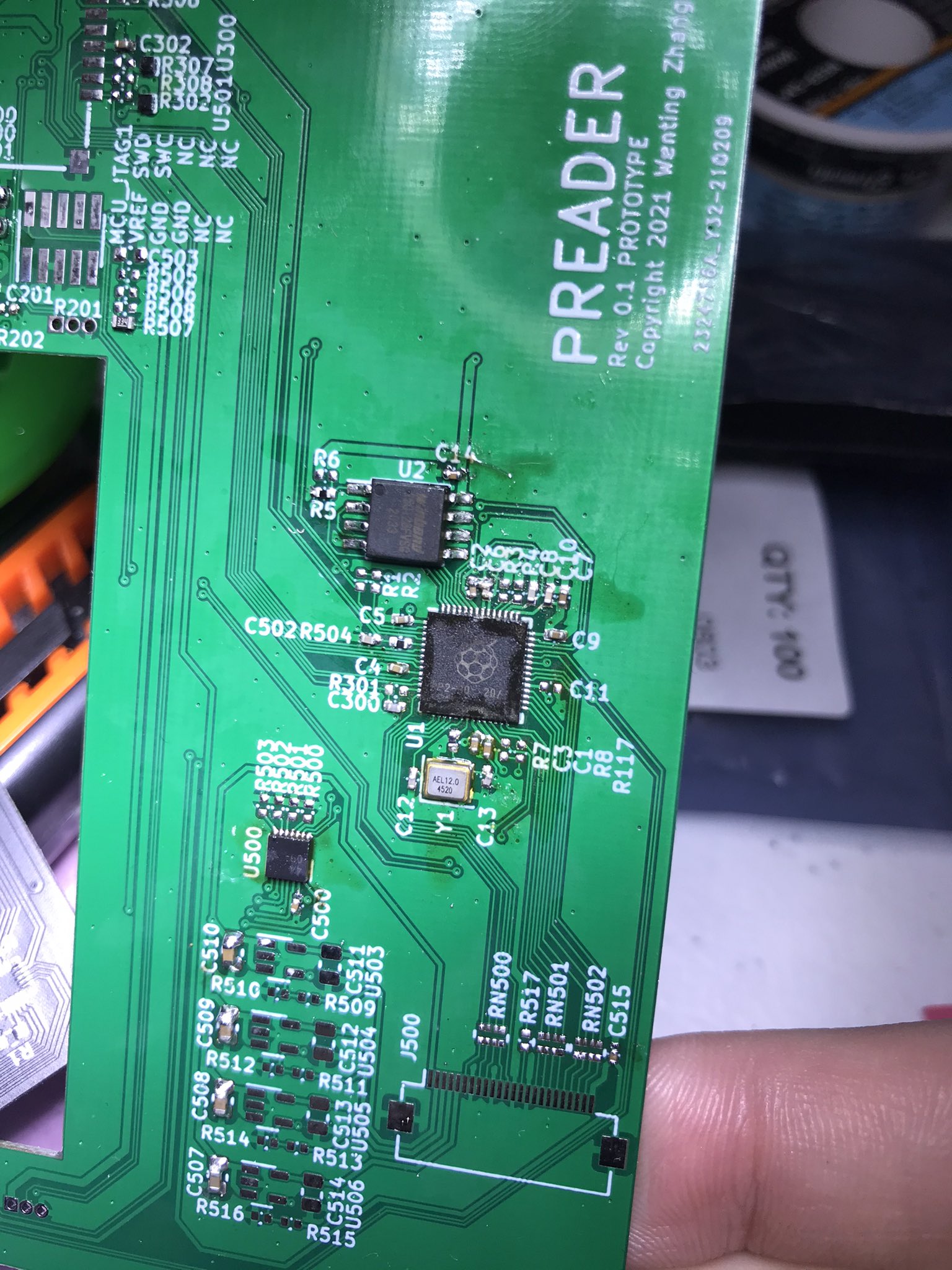
03/10/2021 at 14:30 • 0 commentsSo I have designed the PCB for it:
I am also in the progress of soldering it:
-
Reverse Engineering the Screen
01/30/2021 at 06:02 • 4 commentsOrigin
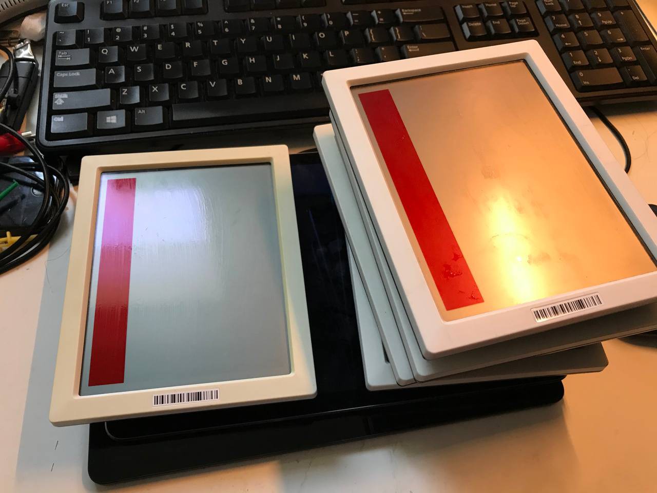
I first saw this screen on the ZBD EPOP 900 electronic shelf label (ESL). Thought it is going to be fun just reverse engineer them, so I bought a few of them:
![]()
PCB
After I got them, the first thing I tried was powering them up. And... I got nothing. After powering ON, they simply wait for the command to be sent over RF. Without knowing the RF protocol, I am simply unable to tell it to refresh the screen, so I cannot just use a logic analyzer to get the details about how the screen is being driven. I would have to start from scratch.
![]()
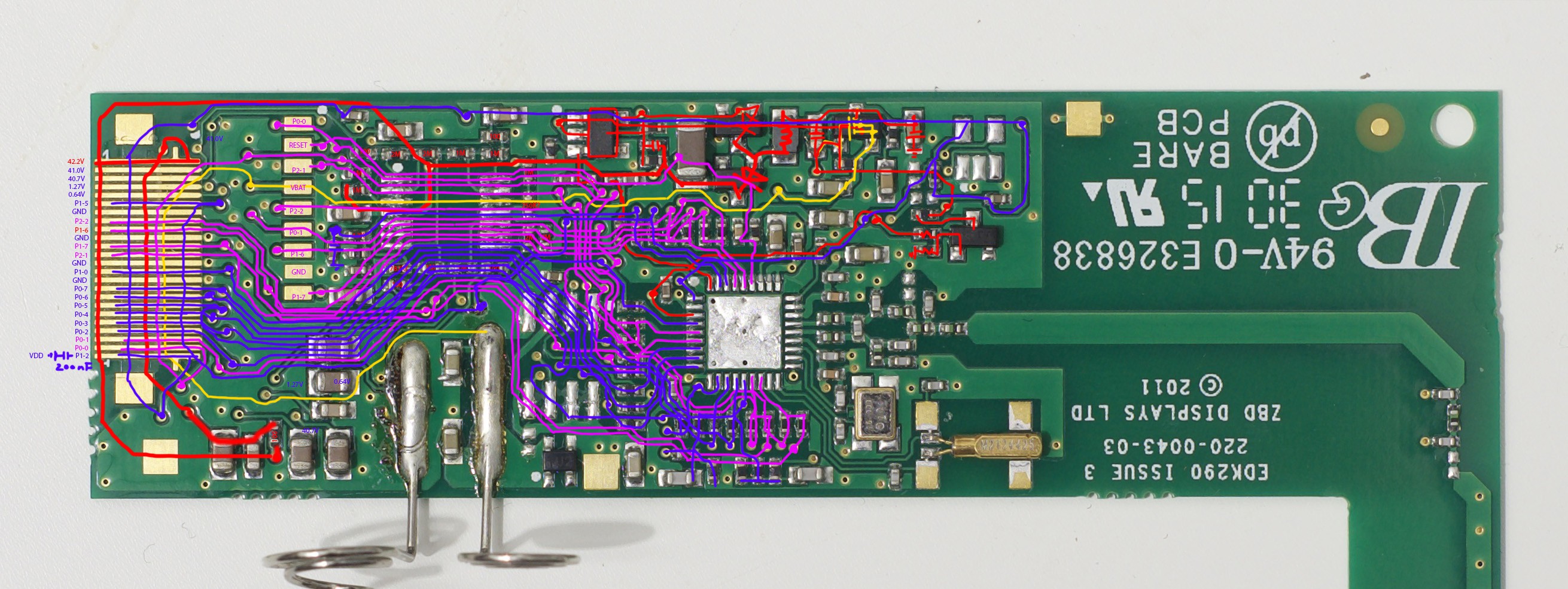
The PCB is not very complex, it is a small 2-layer PCB, with only one TI CC1110 MCU controlling everything. With some tracing, it is clear how the LCD is connected to the MCU. MCU also has control of the LCD voltage regulation and LCD bias generation. These are important information that will be used later.
MCU
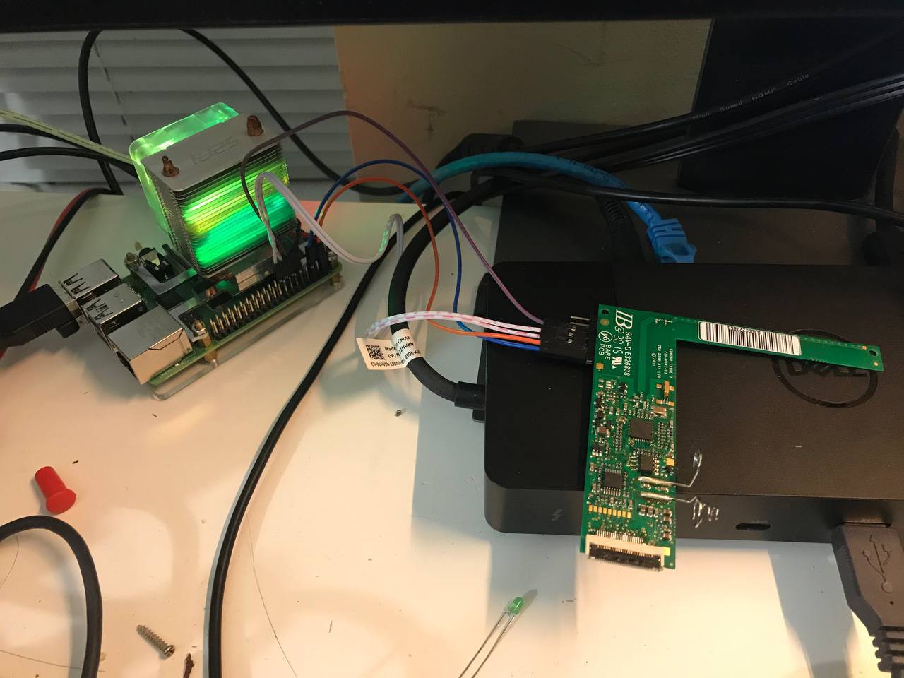
Though I could potentially create my own board or just build a test circuit to drive the screen... but as a first step, I would like to work directly on the original board. So I would need to be able to program the MCU. TI CC1110 has a 8051 core and use the CC 2-wire debugger interface. Unfortunately, I don't have a CC-debugger... but, I have a Raspberry Pi. So with 2 GPIOs I am able to read and write to the internal flash!
![]()
I modified the ccprog utility originally targets the Edison to support Raspberry Pi 4, and you can find the modified version of the program here: https://github.com/zephray/cc1110-prog
With the tool it is also to make backup of the original firmware, so I can flash it back if I ever need to.
For compiling the code for it, I am using make + sdcc. It is available in the Raspbian repository. So, I can directly write my program, compile and download it to the board, all on the Raspberry Pi.
Screen
Now, this is the real hard part. There is no Datasheet or specification sheet I can find online for this screen. The board obviously doesn't tell me more other than where the power rail and the data bus are. The original firmware doesn't want to do anything about the screen unless I have a base station.
There is one hope, though. If I can know the driver IC on the screen, by following the IC pin bump, ITO trace, and FPC cable, I can get the full pinout of the screen. The question is how to know that. Well I don't know. But if I can find a IC, that has the right resolution (channel count), and has the right die size, it is very likely be it. By observing the screen and the traces, it is not hard to see that, they are using 2x240 channel column driver, 1x160 channel segment driver, and 1x240 channel segment driver but only using 200 channels. The 240 channel driver measures 7.6mm x 1mm. From the traces I can be sure it is 240 channel driver, not anything higher.
Of all the 240 channel LCD drivers I can find, here is a list of the die sizes:
- S6B0796: 240 ch 16.2mm x 1.1mm
- NT7704: 240 ch 12.9mm x 1.2mm
- NT7702: 240 ch 11.7mm x 1.0mm
- T66H0001A: 240 ch 14.9mm x 1.0mm
- UCi7702: 240ch 10.6mm x 0.9mm
- IST3026: 240ch 13.9mm x 1.1mm
- S1D17A04: 240ch 13.4mm x 1.3mm
- ST8024S: 240ch 8.6mm x 1.0mm
- ST8024: 240ch 11.2mm x 1.2mm
- ST8024T: 240ch: 13.1mm x 0.7mm
- LC4101C: 240ch: 17.2mm x 2.1mm
None of them matches the one on the screen. That hope is gone.
One thing before I go further, the screen likely doesn't have a controller, but rather only have row and column drivers. This is purely based on experience, I have never seen any monochrome screen with more than 1 COG chips that has controller. If it has controller, it would just be 1 chip, doing both controlling and driving. If it doesn't have a controller, means I will not need to send any initialization commands to the screen. This make me confident that I can drive the screen without knowing much about it.
But how? Well I can always just guess. Here are the control signals usually present on a monochrome LCD without controller:
- VSYNC (Also called FLM), means the start of a frame, reset the column driver to select the first line.
- HSYNC (Also called CL1, or LP), asks the segment driver to latch the input (transfer from input shift register to output)
- Clock (Also called CP, CL2 or XCK), just the data clock for the data bus
- M (Also called FR), a signal only present on passive matrix LCDs, defines the polarity of the driver. Toggle this pin would switch the output polarity. Screens are driven in AC by toggling this pin to avoid polarization.
- EN (Also called ~DISPOFF), turn on or off the driver. This is not the Data Enable on the TFT LCDs, this enables the power, not data.
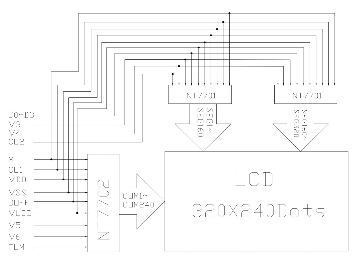
A typical connection diagram should look like this:
![]()
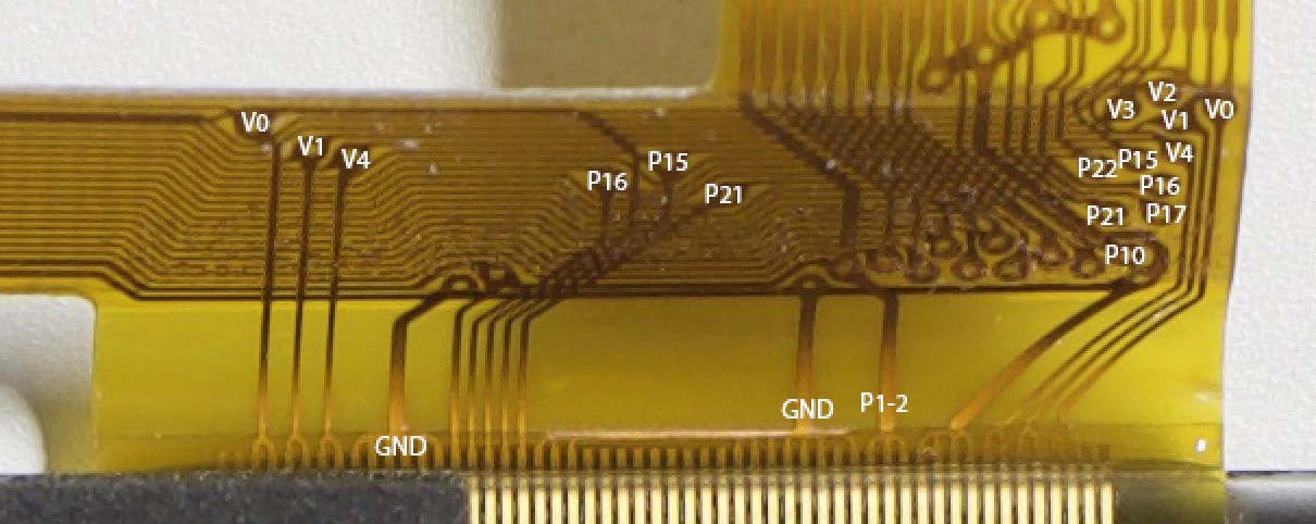
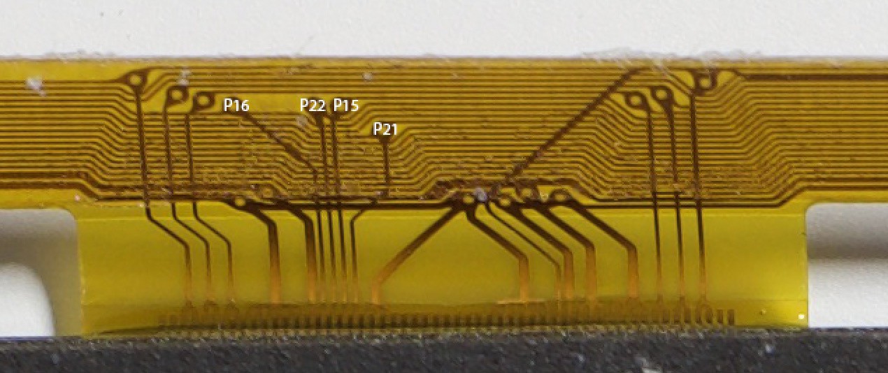
So I expect these pins to show up on this ZBD screen as well. Note this ZBD screen actually has 6 pins, so it probably has additional signal or the signal for segment and common are separated.
There are some additional help I can get from the LCD's ribbon cable, by following the trace there I can know which pins are for the segment, and which pins are for the common.
![]()
![]()
By just looking at the ribbon cable, I get the following list of the pin connection:
- Segment Only Pins
- P10
- P17
- Common Only Pins
- P15
- P22 (Only one of the common driver)
- Shared Pins
- P16
- P21
P1-2 is likely the digital power supply for the screen, because the traces for it are wider, and that line has 2x 100nF capacitor connected.
Just from this list, we can already infer the following:
- P22 is connected to one of the common driver, it must be the FLM/ VSYNC signal.
- XCK must be either P10 or P17.
- LP, M, and DISPOFF are usually shared between two drivers. However I have 4 unconnected signals here. I also only expect 1 pin dedicated to segment and 1 pin dedicated to the common, but I see 2 each here. Means one of the signal is not shared.
- P15 must be that non shared signal, but I don't know which. Similarly, another one is within P10 and P17.
- They likely did that on purpose. I will need to supply the non shared pin with different waveform for COM and SEG.
After hours of trial and error, I get the following:
- Segment Only Pins
- P10 - XCK
- P17 - LP_SEG
- Common Only Pins
- P15 - LP_COM
- P22 - FLM
- Shared Pins
- P16 - M
- P21 - ~DISPOFF
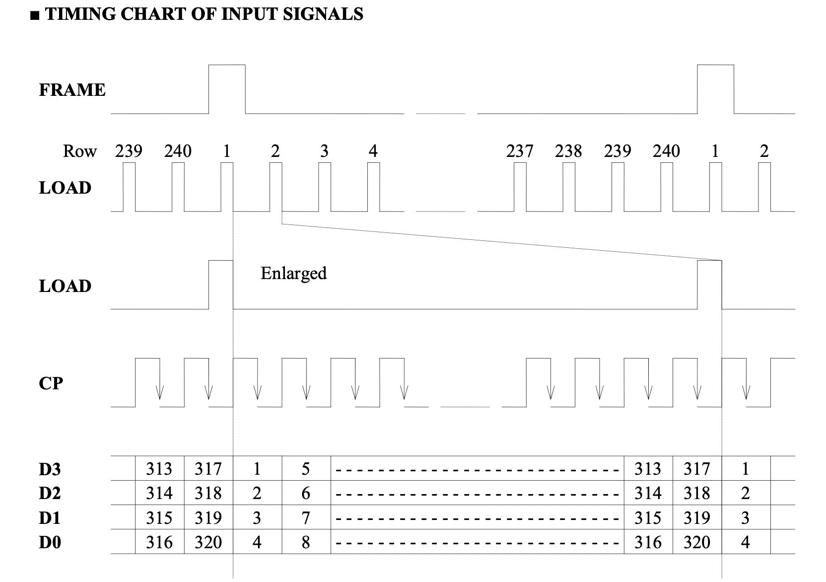
Now on to the timing part. Just like before, start with how standard LCD works.
With a normal STN LCD, the waveform on the control pins should look like this:
![]()
So I tried the same thing here, and it works just fine, given you have the correct delay.
![]()
The issue left seems to be that the voltage is too high. Back to the PCB, actually I have traced out that there are 2 pins that are being filtered by a 1st order RC filter and connected to the power supply circuit. P1.3 controls the voltage of DCDC output, and P1.4 controls the voltage of bias generation. RC filtering suggests that they are actually PWM signals. Yes, indeed these two pins connects to the TIMER 3 compare output. After setting the voltage lower, I can get a clear image (see the project album).
Source code for the driver so you could reproduce this on your own board:
https://github.com/zephray/zbd-epop-900-screen-demo/blob/master/main.c
Notes
Well it might sound like it was quite easy reverse engineer it, it was not. I wasn't aware that the voltage was controllable (thus not aware that I have the voltage entirely wrong), and I didn't realize that both P15 and P17 are both LP at first, caused lot of confusion at first. At the end I spent lot of time fighting with air. I am glad eventually I have sorted everything out.
Bistable LCD e-Paper eReader
eBook Reader based on Raspberry Pi RP2040 MCU and ZBD Bistable LCD