This is the primary timing generator.
Rather than trying to capture screenshots of my logic analyser, it is easier and quicker to write a small C program to simulate it. So I did. See file J031-U27-analyser.c.
The waveforms look like this (state at the bottom, data above, white shaded is one MPU cycle):

from which we can deduce:
- The MPU cycles every 24 clock ticks.
- For a 28 MHz clock, the MPU cycles at 28/24 = 7/6 = 1.166 MHz.
- That gives exactly 224 MPU cycles per 64 microsecond line.
- And 160 MPU cycles of display time are 45.714... microseconds.
- MPU clock duty cycle is 11 high to 13 low.
- There are four /RAS cycles, each six clock ticks long.
- Three happen when VCYC is high (video access)
- One happens when VCYC is low (MPU access)
- States 1, 3, 5, 7, 10, 18, 20,25 are illegal, and sweep to state 0.
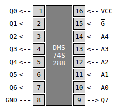
The DMS72S288 pinout is:
 I had a long hard look at the binary sequencing, the see if it could be implemented in a 16V8 GAL.
CYC3 is easy, inverting every clock cycle.
The rest do not have an obvious pattern. The PROM allows any random sequence. A GAL would have to decode 32 OR terms to do the same. I expect the designers wanted to keep the flexibility to cope with potential changes. I think I'll leave this part of the circuit for now.
 Keith
Keith
Discussions
Become a Hackaday.io Member
Create an account to leave a comment. Already have an account? Log In.