The simplest way to use a phototransistor is to hook it up with the collector connected to a voltage supply, and the emitter connected to ground through a resistor. As more light hits the phototransistor, it conducts more current, and so the voltage across the resistor increases.
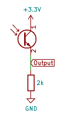
You can adjust the sensitivity of the circuit by adjusting the value of the resistor. Higher values provide higher sensitivity, but at the cost of slower response times.
For example, here is the key activation waveform for a problematic switch I was investigating, which was using a 1k resistor.
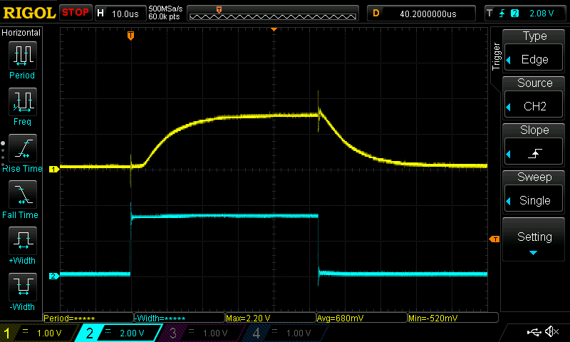
Channel 2 (blue) is the selector for that that cluster, so a high value essentially enables/energizes the cluster, and a low value disables it. And channel 1 (yellow) shows the output voltage of the phototransistor when the key is in a pressed state, based on the above circuit.
As you can see, this particular switch is only reaching about 1.5V at its highest value, which is not high enough to register as a logical 1 value. And the rise and fall times are already a bit sluggish, at around 30us.
Swapping out the resistor for a lower value (470), we get the following:
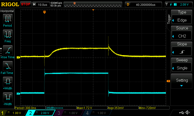
The rise and fall times are much improved, but the sensitivity is even lower, and the max voltage doesn't even reach 1V.
Going the other direction, here is what we get with a 2k resistor:
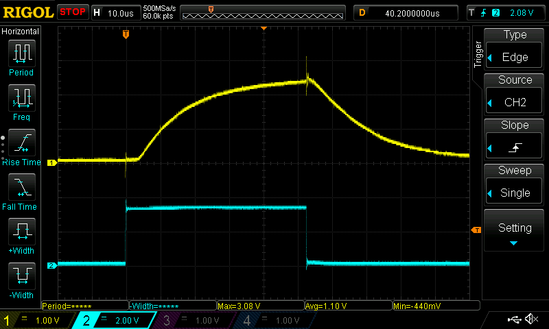
This is starting to look promising, with the max voltage reaching over 2V, which is the minimum required to register as a logical 1. However, the rise and fall times are now even worse, taking a full 50us before it starts leveling off.
I had a bit of trouble with this particular key in the previous design as well. The problem is that the key travel is very short, and the key stem doesn't entirely get out of the way of the light path, so less light is reaching the phototransistor. I solved this in the previous design by boosting the current/brightness of the LED for that switch, but even that wasn't enough to get a fast/high enough signal from the phototransistors in the new design.
The issue is likely the wider key stems in the new design. This increases the distance between the LED and phototransistor, and so even less light is reaching the phototransistor, and it's just not able to get enough light.
And this is where the transimpedance amplifier (TIA) comes in. It's a fancy name for a particular arrangement of an opamp, such that it converts a current-based signal (like that from a phototransistor) to a voltage-based signal (like what is needed on a gpio pin). The main benefit in this application is that it has a very low input impedance. And similarly to when we swapped out the resistor in the first circuit for a lower one, a lower input impedance means that the phototransistor is able to respond more quickly. And, critically, the input impedance is independent of the sensitivity/amplification factor.
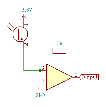
In this circuit, the 2k resistor serves a similar purpose as the resistor in the first circuit. A higher resistor value increases the amplication and results in a higher output voltage. But without affecting the rise and fall times of the phototransistor, because the phototransistor still "sees" the opamp's low input impedance.
And here's the key activation waveform after switching to a TIA.
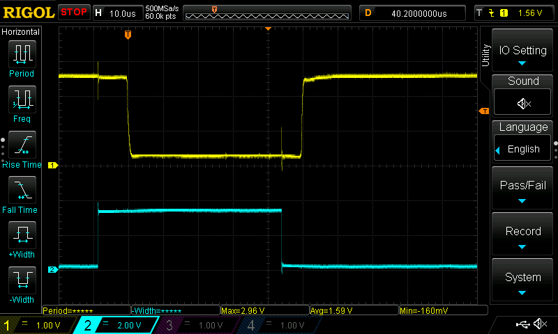
One thing to note is that the TIA inverts its output. So instead of a low-to-high transition when a key is pressed, it is now a high-to-low transition. And both the high and low voltage levels are at comfortable logic levels.
As you can see, the response time is much quicker now, with the voltage leveling out after only ~10uS after the cluster is enabled.
The above was with a 2k feedback resistor in the TIA circuit. Just for comparison, with a 470 ohm resistor instead, we get:
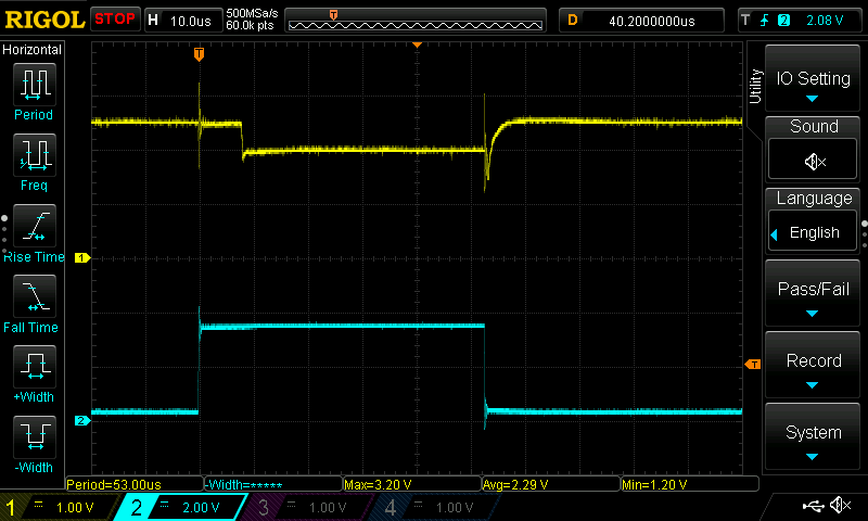
The sensitivity is lower as expected, with the low voltage level only being about .5V below the high voltage level. But the response time is largely unaffected.
Using TIAs for the new design has a few advantages
- It's able to deal with that pesky thumb switch that doesn't get much light
- It minimizes the response times of the phototransistors, which allows for shorter duty cycles (and thus less power usage) when scanning through the matrix.
- It boosts the sensitivity of the phototransistors, so the LEDs can be driven at much lower current/brightness. The original design drove them at around 25mA each, with 5 LEDs lit at a time per side, for a total current draw of 250mA. But with the increased sensitivity, I can drop the current down to around 5-10mA each*, for a total draw of only ~50-100mA.
(* except for the problematic switches on the thumb clusters)
 Ben Gruver
Discussions
Become a Hackaday.io Member
Create an account to leave a comment. Already have an account? Log In.
The waveform with the TIA looks very clean! Does that mean that debouncing isn't necessary? Huge plus for gamers and simpler firmware.
Are you sure? yes | no
Yep! No debouncing needed.
Are you sure? yes | no