So I've been working on this for a while already and am only now catching up in documenting it. I document it because it might be useful to someone but also because it tends to be useful to myself, if I need to check back later on what exactly happened, when, or why I did things a certain way.
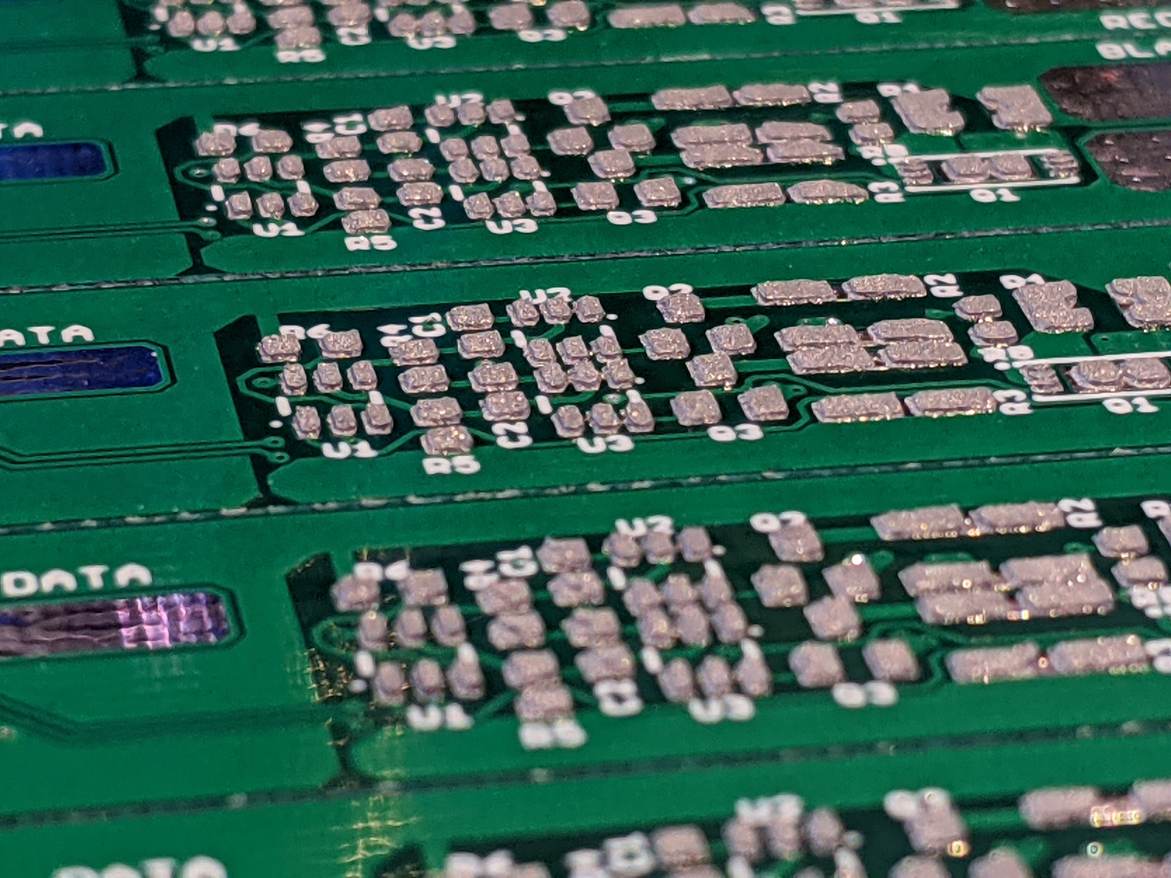
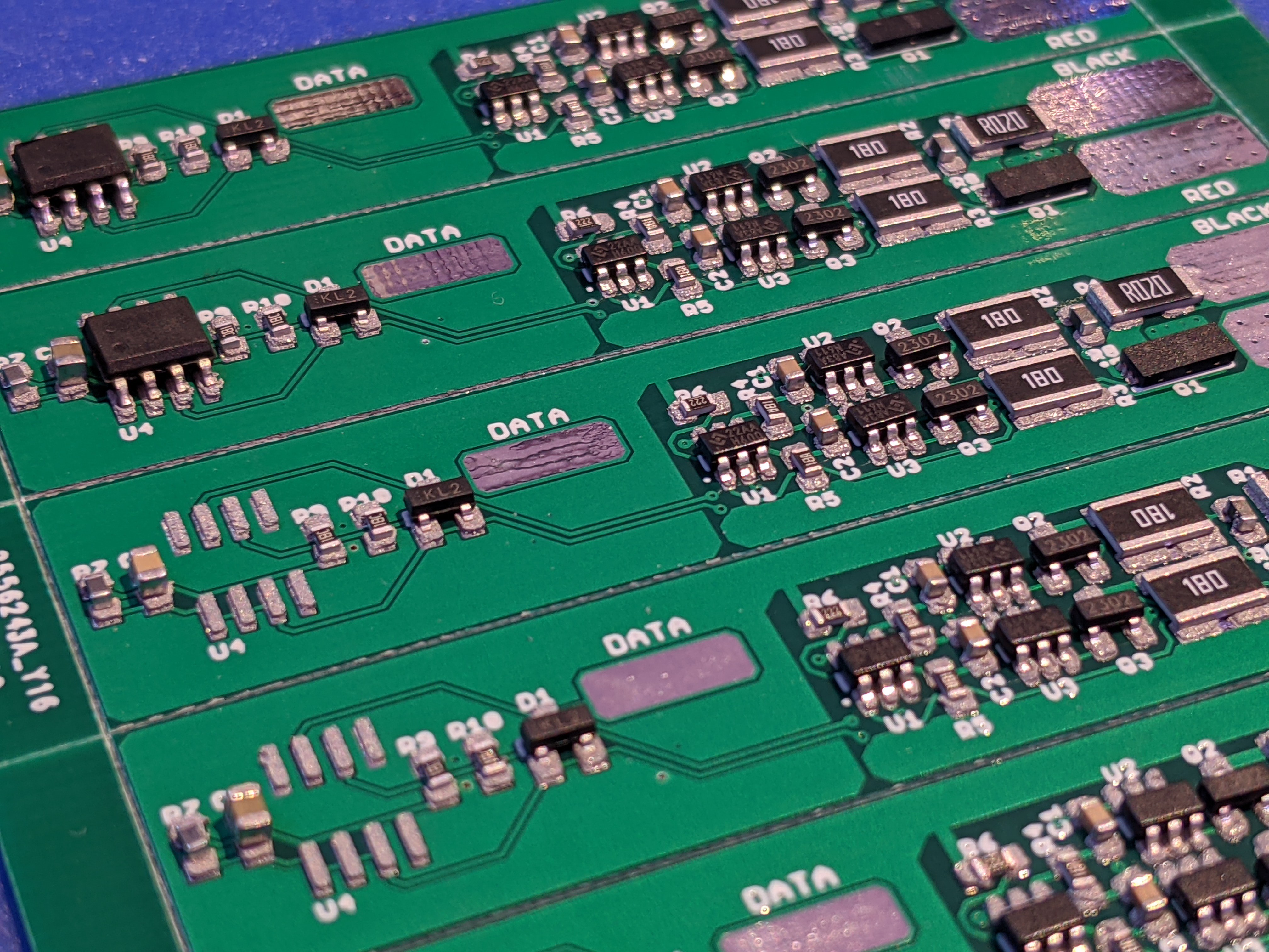
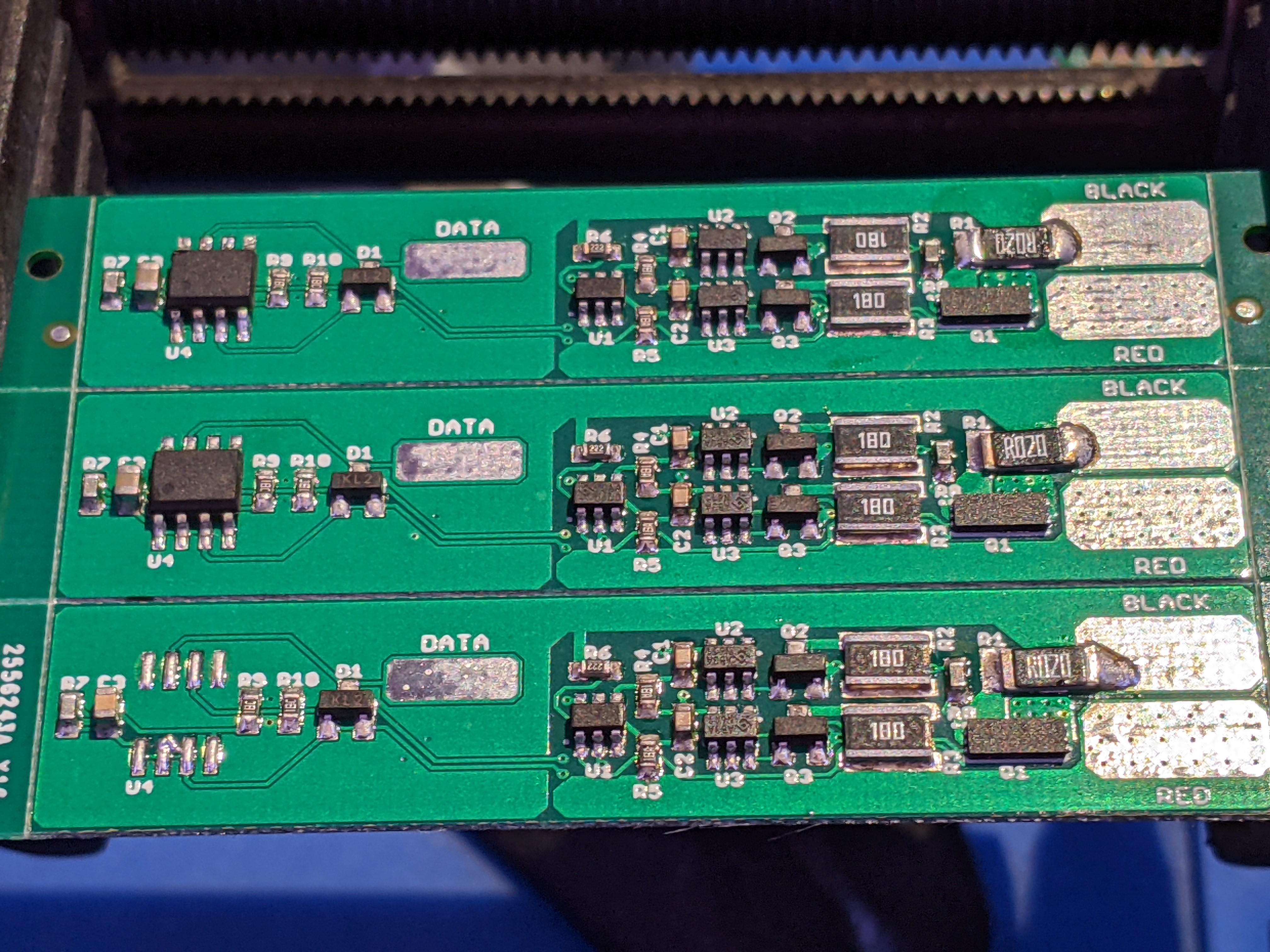
I think it was last week that my prototype PCBs and parts for the first 2S LiFePO4 BMS arrived and this effort really started to accelerate. Here are some pictures of the prototype build:


This was a small panel with 5 identical circuits (3 left in the bottom picture).
Each circuit has roughly two parts to it: on the right there is the fairly standard pack protection and balancing. It uses two HY2212 chips with MOSFETs and 18Ω resistors to burn off excess energy if a cell reaches 3.6V. The resistor value makes it so only 200 mA can be burned off, to keep resistor wattage/cost and heat generation in check. This means that when we reach that point, the charger should only try to put in 200 mA max, because otherwise the cell will still get the remaining current. So the charger has to take part in this for it to work. Then there's also an HY2122 chip which takes care of protecting the pack from over voltage, under voltage, over current and short circuit. It uses Q1, a dual, drain connected MOSFET to turn charging and discharging on and off. It normally measures the voltage across this dual MOSFET to determine current limits, but I decided to have lower RdsON MOSFETs and add resistor R1 to make these limits more predictable since RdsON of MOSFETs can vary quite a lot and the limits depend on the total resistance. As you can see, I messed up the part I bought so there's a 2010 size resistor where there should be a 1210. Oh well, it still fits. :)
The left side of the circuit is where most of my "special sauce" is. The SO8 chip is a Padauk PMC131 microcontroller, which implements the 1-wire digital interface in software, contains the pack ID data and can measure the two NTC thermistors. Yes, I admit it, I like these little Padauk micros. I used one very effectively in my #wESP32. This one has a little more oomph and costs a little more than the 3¢ PMS150C that made them famous, but you still get a lot of value for the price. In this case, a 12-bit ADC and -40°C to 85°C temperature range.
To be honest, I had some trouble making the 1-wire protocol work in this chip. Unlike some other protocols, 1-wire is very dependent on timing, with a 1 being a short pulse and a 0 a long pulse. It took a good deal of optimization to make everything execute fast enough. I also ran into an issue because I was testing the code using a MicroPython 1-wire host running on a Raspberry Pi Pico, and it turns out that the timing of the MicroPython onewire library is just wrong. It doesn't respect the minimum bit slot time of 60 μs. It also doesn't wait for a low bus to be released before it starts pulling it low for the next bit, but just clobbers through what the slave is doing. I forked the code, fixed it and flashed my own version and then it worked. I should do a pull request to get this fixed upstream, but the fact that there are currently 377 open pull requests doesn't make me feel optimistic that it would be useful. I should still do it though.
R7 on the far left and R8 next to the balancing resistors are both NTC thermistors that are measured by the micro, and their value in a resistive divider can be read over 1-wire. I have two of them to hopefully be able to tell more about the pack state. R7 is far from the balancing resistors and R8 is right next to them so I hope to be able to tell from the temperature gradient when one of the balancers kicks in.
The components and wiring pads are all clustered toward the center of the PCB because I want them to face inward and end up in the gap between the cells. To make some use of that wasted space between the cells that offends me. ;)
 Patrick Van Oosterwijck
Discussions
Become a Hackaday.io Member
Create an account to leave a comment. Already have an account? Log In.