Close
0%
0%

Hexo

Six "sided" LED Randomizer a.k.a. an electric die

Public Chat
Similar projects worth following
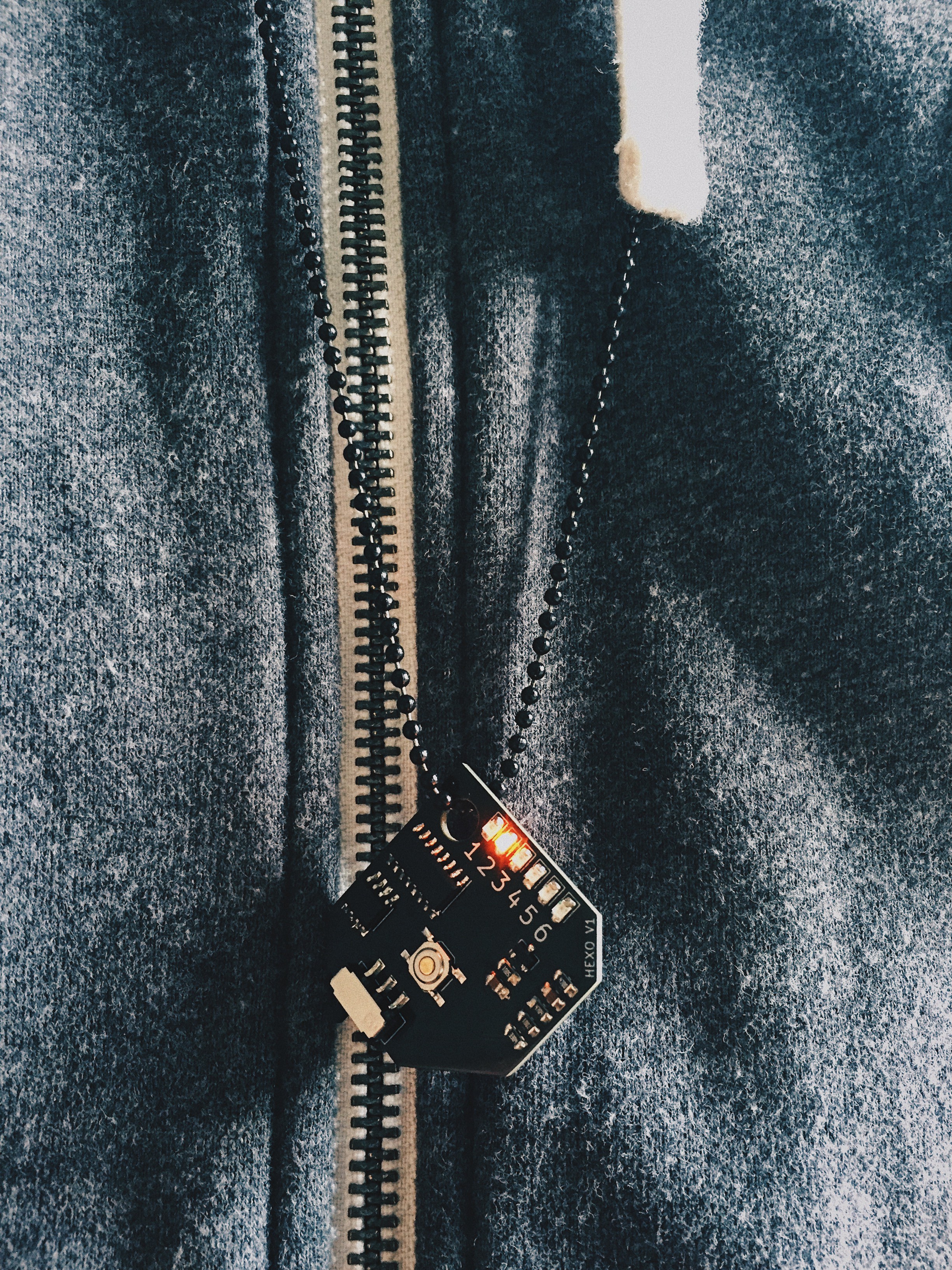
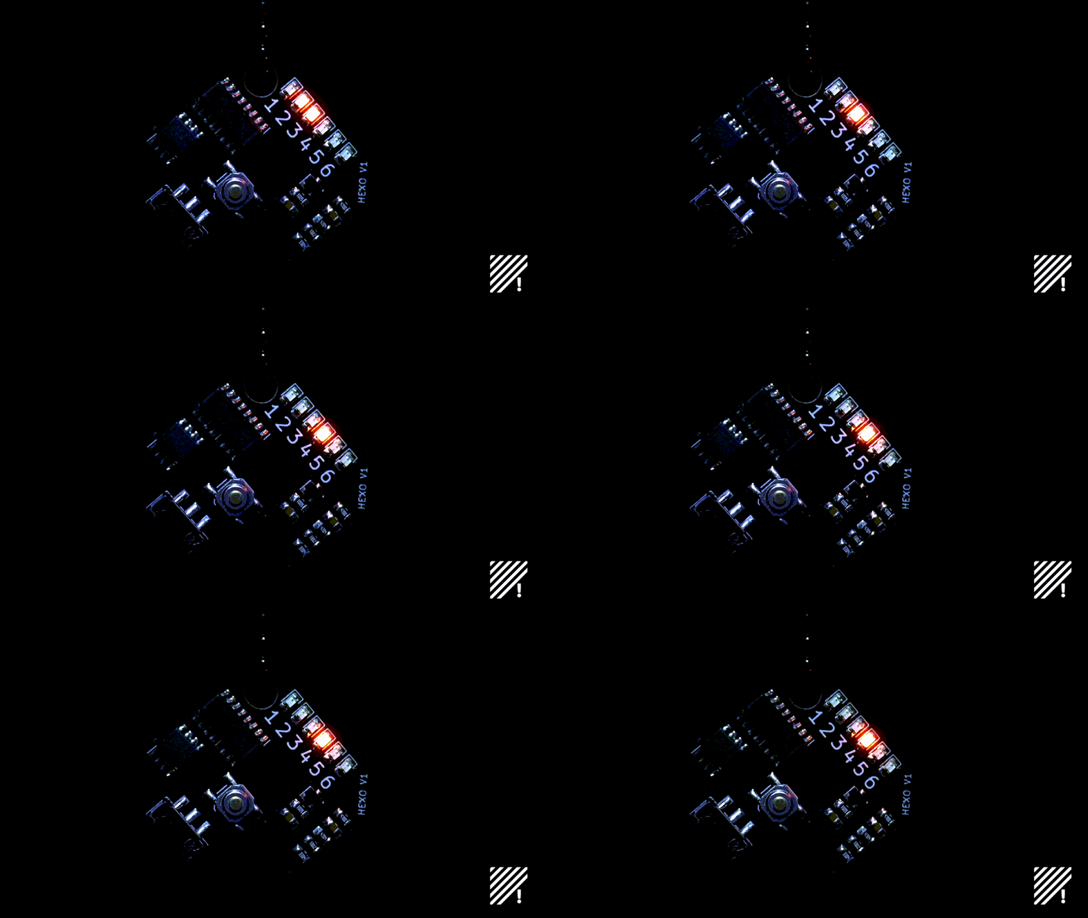
This project is uses an iconic 555 and CD4017 to randomly illuminate one of six LEDs. This project is my first analog circuit, my first use of a 555, and my first PCB! I wear Hexo everyday—it makes for a great conversation starter!

Hexo, a play on hexa- as in the prefix for "having six", is a circuit that uses a 555 and CD4017 to randomly illuminate select one of six LEDs, similar to a die. By using a capacitor and transistor, the circuit will toggle through the six LEDs, flashing them in sequence, and then slowly reduce the frequency until only one is left on.
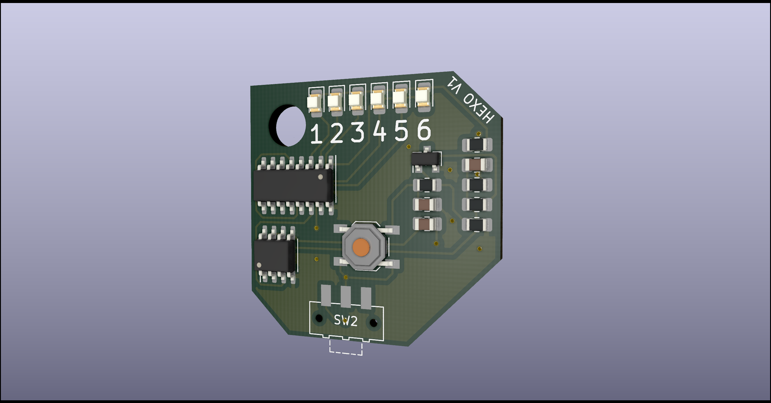
Motivation

Hexo is a project designed to help me understand the steps of circuit design, prototyping, schematic capture, simulation, PCB layout, PCB manufacture, ordering, and assembly. This is my first analog PCB project and was inspired by Contextual Electronics' Getting to Blinky 5.0. I was very excited to have my first project use the 555, a ubiquitous stable of hobby electronics, but I wanted the circuit to do a bit more than blink.

How it works
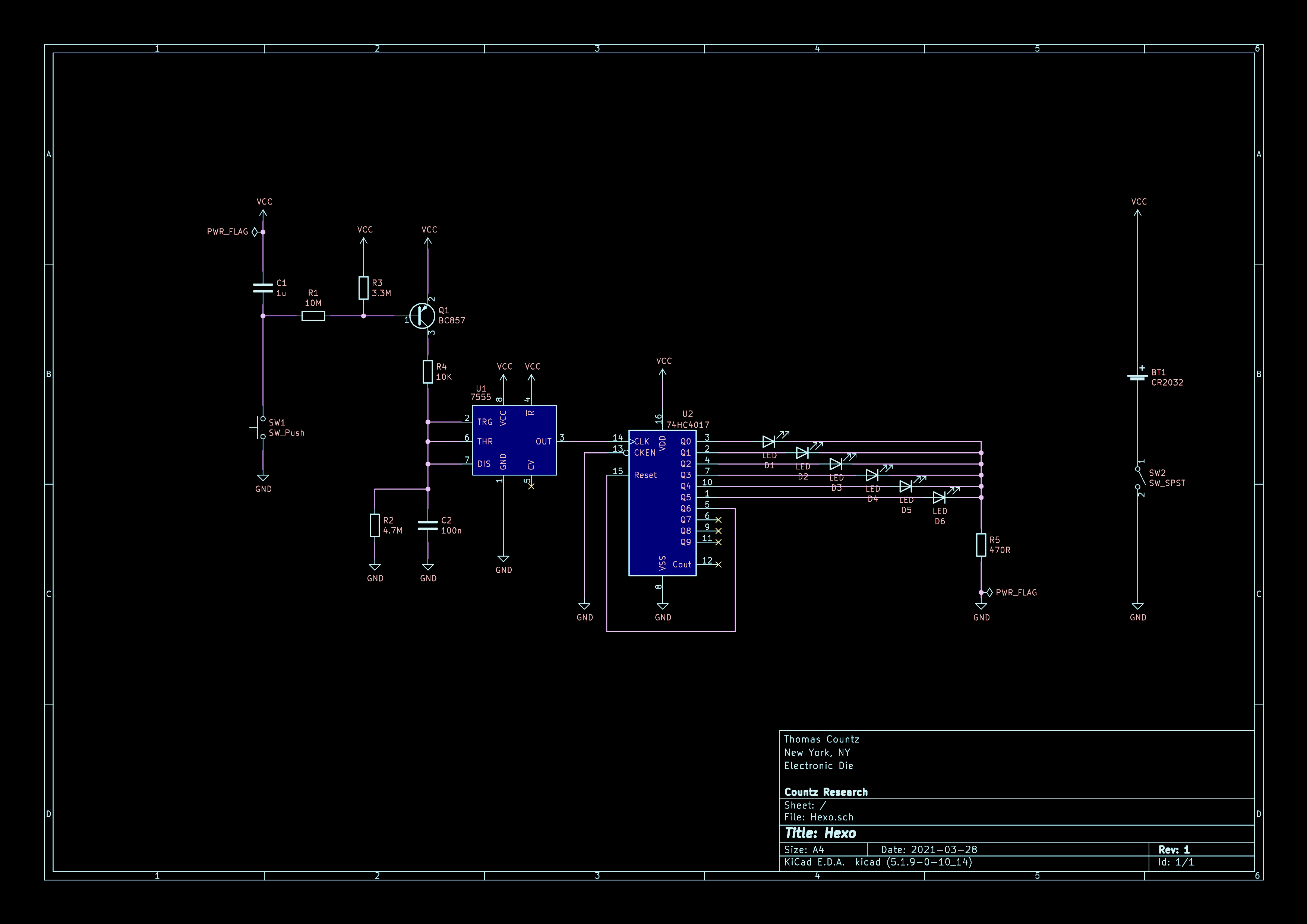
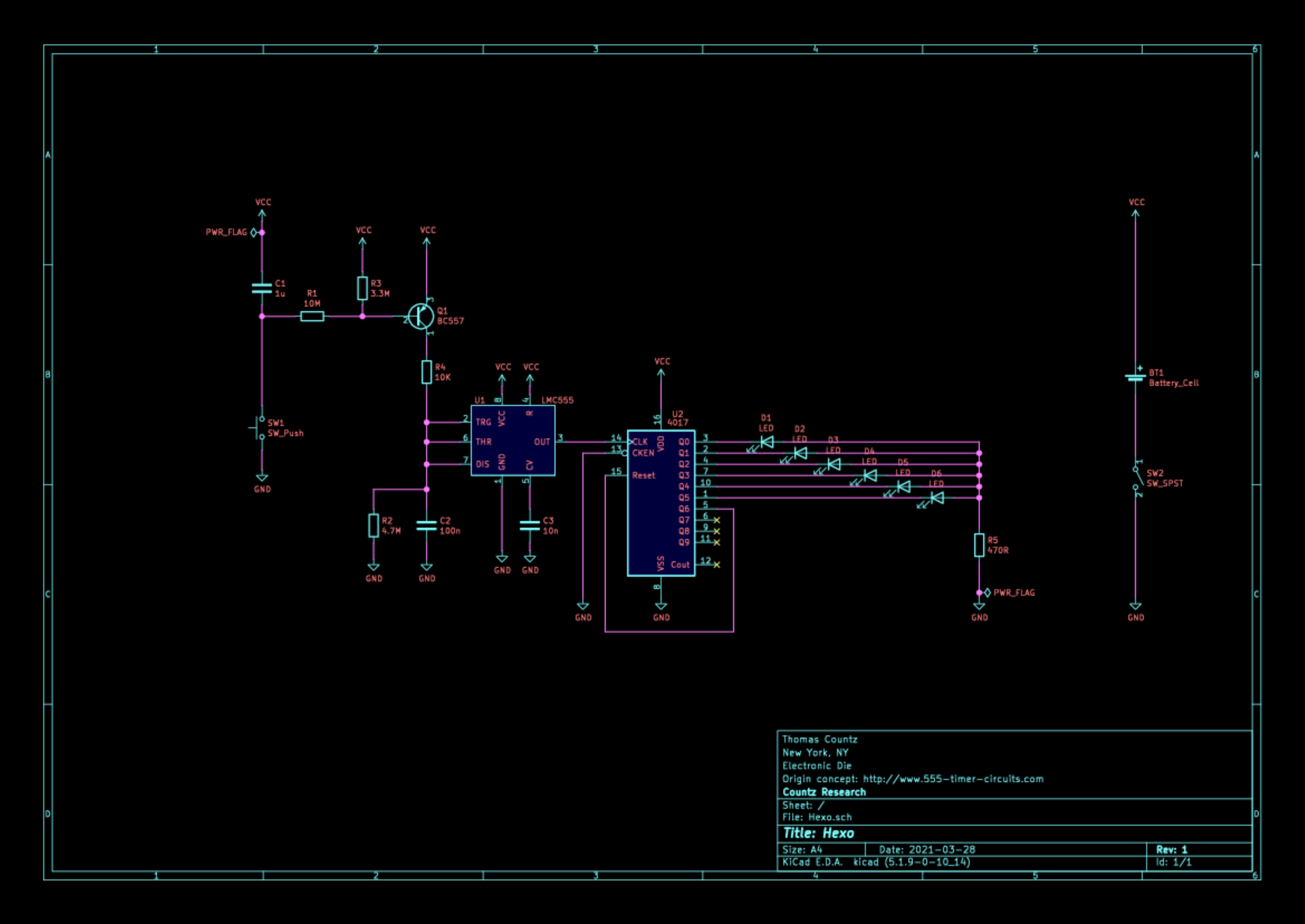
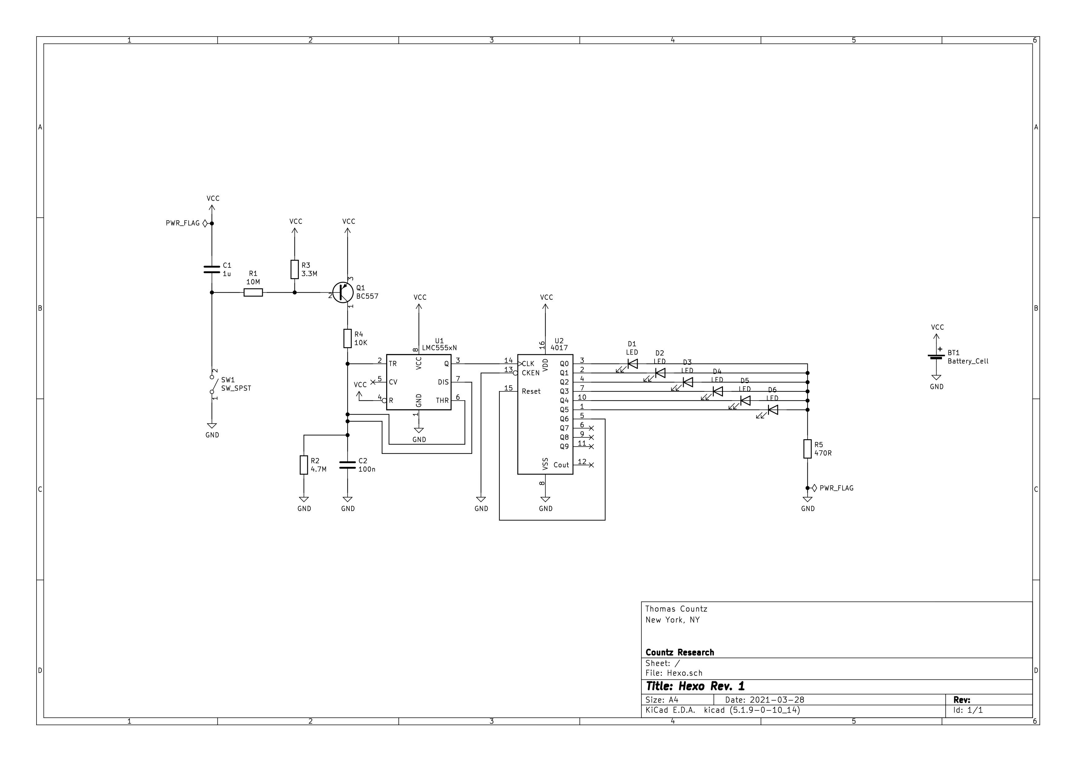
You can find the PDF version of this schematic under the project's documents.

When SW1 is closed, C1 quickly charges to VCC (I think there might need to be a current-limiting resistor between C1 and VCC, though maybe SW1 provides this). After C1 is charged, current begins to flow from VCC through both R3 and the Q1's emitter. Because Q1 base voltage is negative w.r.t. the emitter voltage (Q1 base-emitter voltage), the transistor is active forward and current flow through the collector. (It's a PNP).
Let's continue as if SW1 is still closed. Now that current is flowing through Q1, the 555 begins to oscillate as if it were in astable mode. Charging and discharging C2 to 2/3 and 1/3 VCC respectively and setting pin 3 (output) high and low in kind.

 Pins 2 (trigger) and 6 (threshold) are tied together so that the 555 can continue to "retrigger" itself when C2 is discharged and the voltage reaches 1/3 VCC. In a typical astable configuration, a resistor is placed between pin 7 (discharge) and tied-together pins 6 (threshold) and 2 (trigger). This has the effect of adjusting the duty cycle by altering the charging speed of C2. In this circuit, the duty cycle is manipulated by altering the charging speed of C2 by way of a steadily reducing current through Q1 instead.

Now that the 555 is oscillating, pin 3 (output) sends a square wave clock pulse to the 4017 pin 14 (clock). The 4017 is a decade timer and at each rising edge of the clock pulse it will consecutively set each of it's 10 output pins high. Only one pin is high at a time, the other are low. In the case of this circuit, we're only interested in using 6 of the 10  outputs, so we tie pin 5 (Q6), the seventh pin to be set high, to reset which will cause the 4017 to set it's first output (Q0) high instead.
All of these outputs are used to drive LEDs which whose cathodes are connected to a common current limiting resistor before being tied to ground. These LEDs will continue to be turned on and off consecutively as long as a clock pulse continues to drive pin 14 (clock).

Let's continue now as if SW1 is opened after being closed. Once SW1 is open, C1 begins to discharge and current continues to flow through VCC and GND by way of Q1. As C1 discharges, however, Q1 base-emitter voltage begins to climb, i.e. the base voltage starts to become less negative w.r.t. the emitter voltage. As this is happening, less current is flowing through Q1 and C2 is taking longer and longer to charge and therefore the clock pulses from pin 3 (output) of the 555 are beginning to slow (the time between clock pulses is increasing). This has the effect of diminishing the speed at which the 4017 is cycling through the LEDs.

Eventually, Q1's base-emitter voltage reaches the cutoff threshold (~-0.6v) and current stops flowing through Q1. C1 continues to discharge, however, through R3. At this point, whichever LED the 4017 had set to high last, remains lit.

I'll include a simulation in the next update so that you can see all of this in action with either LTspice or Falstad.

Stages

Circuit Design. For this project, the circuit design comes by way of 555 Timer Circuits' roulette and dice circuits.

Prototyping....

Read more »

Hexo.pdf

Revision 1 schematic

Adobe Portable Document Format - 24.81 kB - 04/26/2021 at 22:33

Preview

gerbers.zip

Revision 1 gerber files

Zip Archive - 31.14 kB - 04/26/2021 at 22:30

Download

hexo.asc

LTspice circuit simulation. YOU MUST INSTALL THE LIBRARIES AND SYMBOLS FROM CD4000.zip

plain - 4.02 kB - 03/28/2021 at 18:39

Download

CD4000.zip

CD40xxx spice model library for LTspice from www.linear.com/software

Zip Archive - 38.80 kB - 03/25/2021 at 01:38

Download

falstad_hexo_simulation.txt

Import this file into https://www.falstad.com/circuit/circuitjs.html to run the simulation

plain - 2.06 kB - 03/28/2021 at 18:30

Download

  • 1 × 7555 Inductors, Chokes, Coils and Magnetics / Pulse, Signal, Datacom, Telecom Transformers
  • 1 × 74HC4017 Electronic Components / Misc. Electronic Components
  • 1 × BC857C Discrete Semiconductors / Transistors, MOSFETs, FETs, IGBTs
  • 6 × LED Fiber Optics / Emitters
  • 1 × 100nF Ceramic Capacitor Ceramic Capacitor

View all 14 components

  • Lucky Number Four

    Thomas Countz04/28/2021 at 00:27 0 comments


    Here's a GIF of Hexo! This project is complete!

  • Meet Hexo.

    Thomas Countz04/21/2021 at 19:33 0 comments

  • PCB Delivered!

    Thomas Countz04/18/2021 at 16:11 0 comments


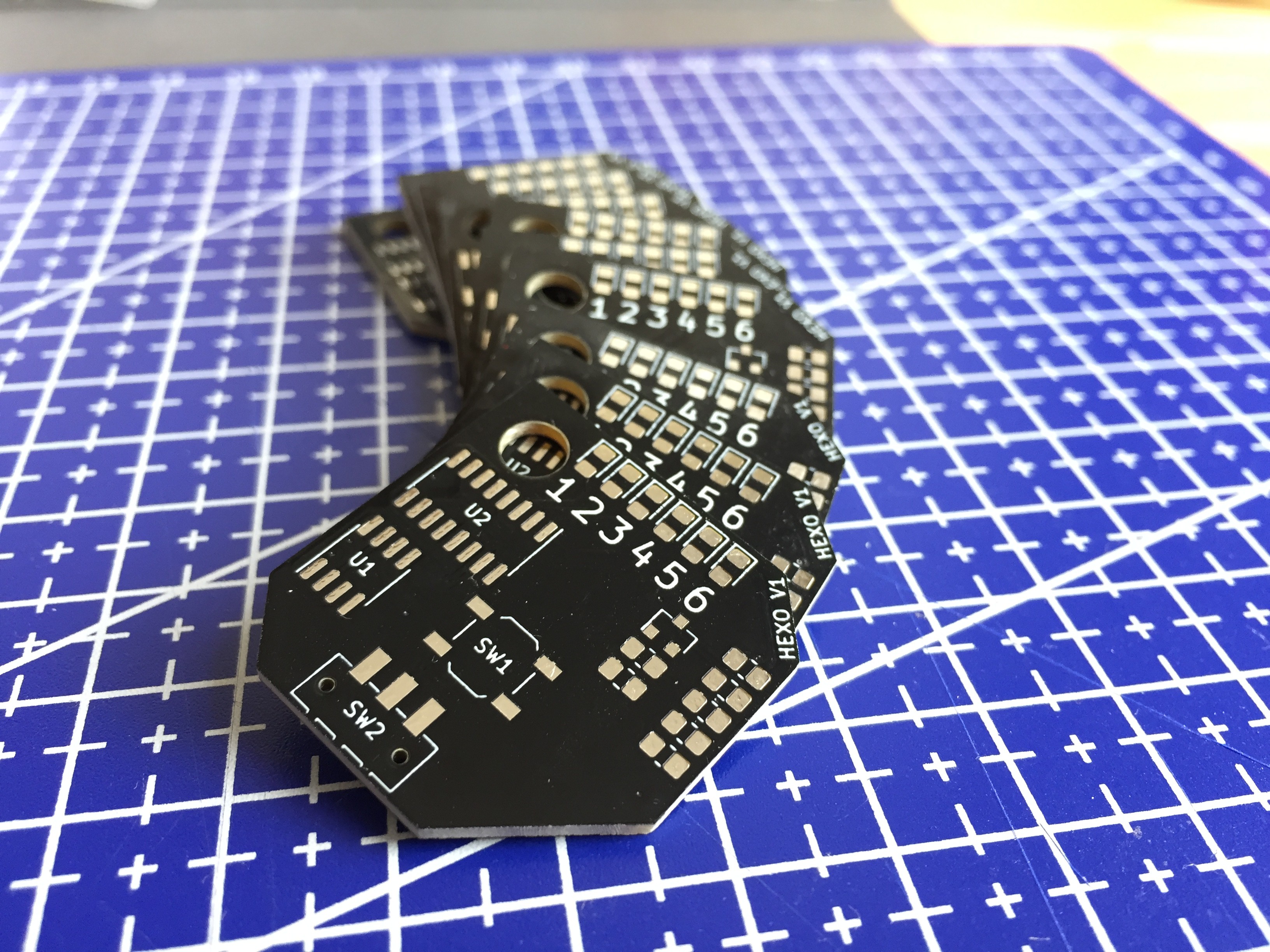
    I just received my order from PCBWay in 6 days!! They all look great!

    Next steps: assembly (although I'm waiting on flux...)

  • Parts Received!

    Thomas Countz04/16/2021 at 00:50 0 comments

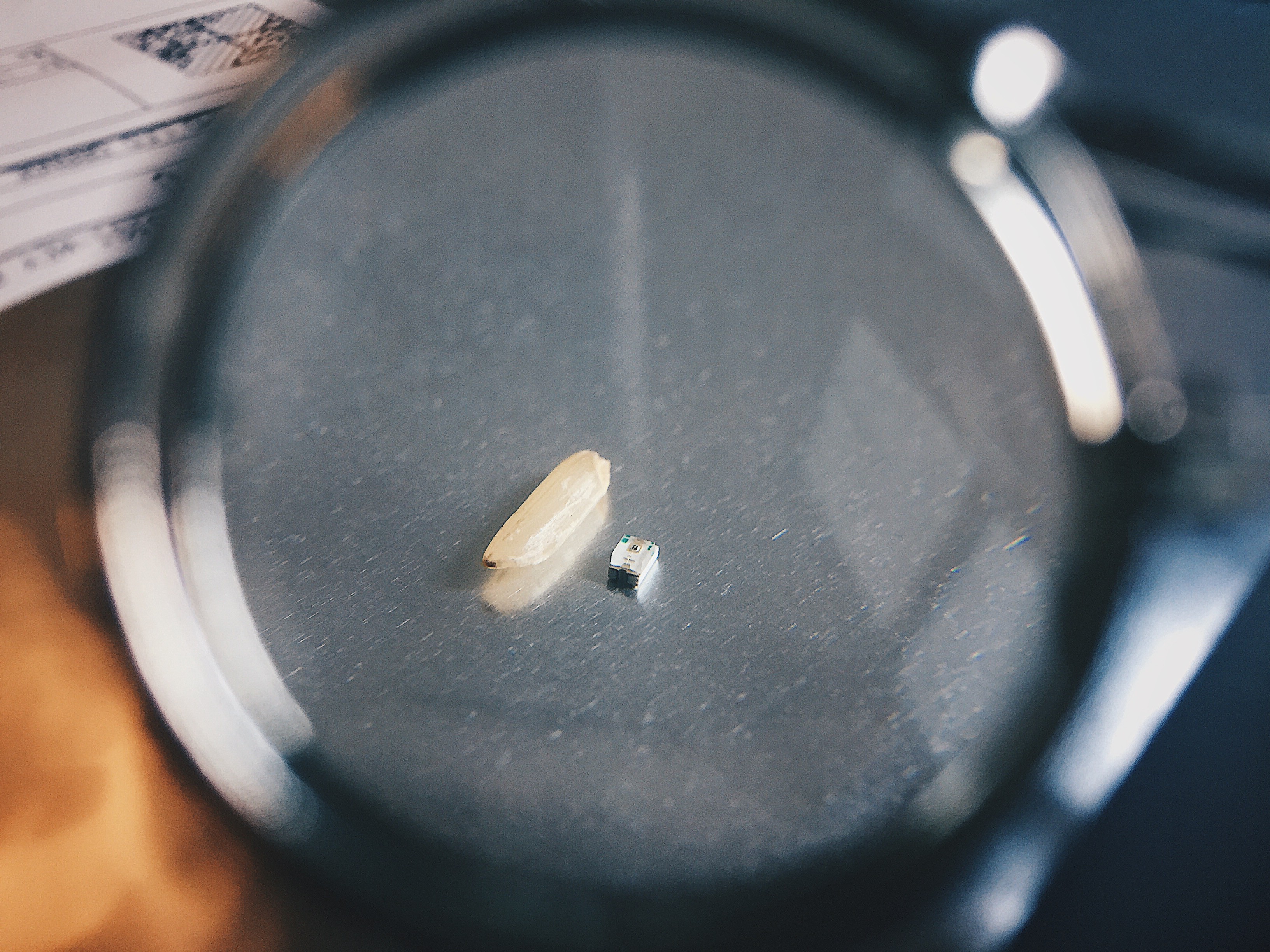
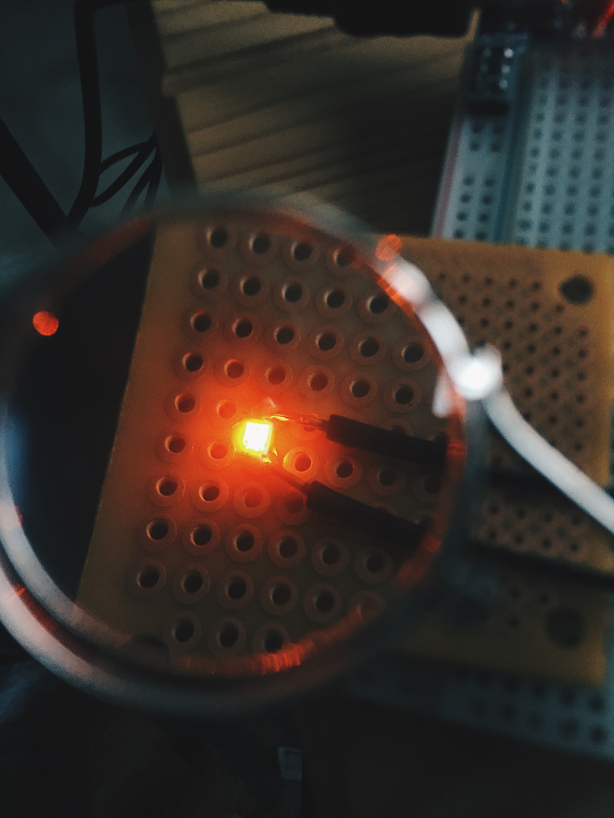
    I'm still waiting on the PCBs (ETA: April 21), but for now, I tested out some of the LEDs. I hoping the orange really pops against the black solder mask. 0805 is tinier than I thought so I made sure to order a new flux pen!

  • Gerbers Submitted

    Thomas Countz04/11/2021 at 01:48 0 comments

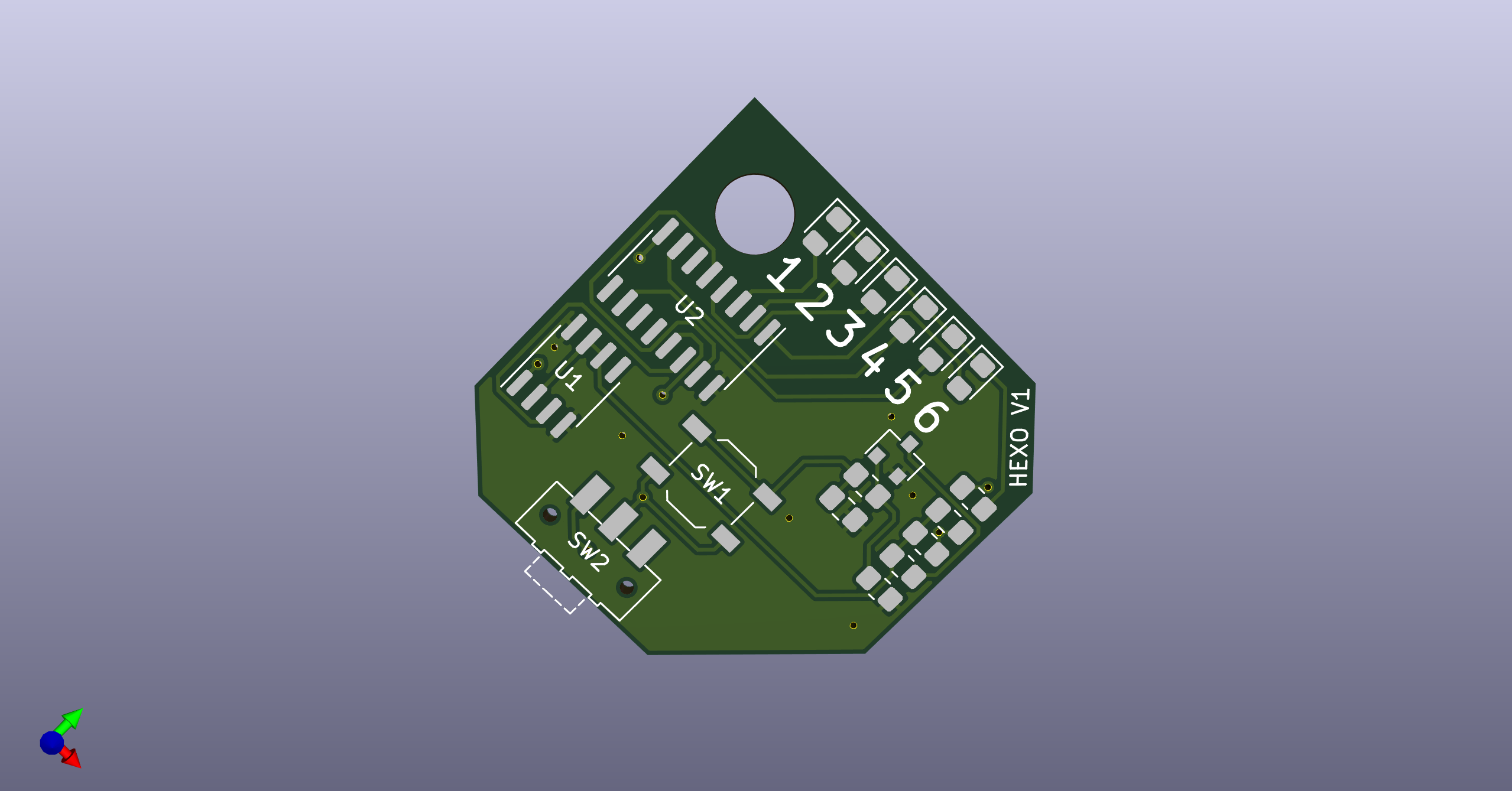
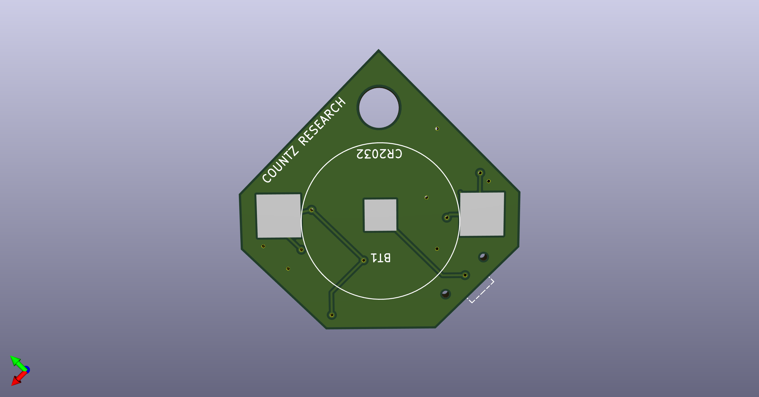
    Today, I've touched up the design a bit and sent off the gerbers to PCBWay for review!

    This has been an exhausting amount of work so far, but I've learned A TON already. Without a lot of experience, it's hard to tell whether or not the board will work when it shows up, but I'm excited to find out. I'm thinking that at the very least I'll need to experiment with the resistor and capacitor values to get the LED timing and battery usage right.

    My order from Futurlec still hasn't shipped. I contacted them a week ago and they said they're still working on it... my plan was to have those parts here by now so that I could run experiments on powering this circuit with only 3 volts, but it'll have to wait for the first run of the PCBs—I wouldn't be surprised if they show up first.

    If all else fails, I hope that I end up with some cool PCB pendants and a heck ton of knowledge!

  • Oops.

    Thomas Countz04/04/2021 at 19:45 0 comments

    After finishing the layout, I started doing some electrical checks and the first thing I noticed was that I wired in all of the LEDs backwards.

  • PCB Edge Cut Calculations

    Thomas Countz04/04/2021 at 15:51 0 comments


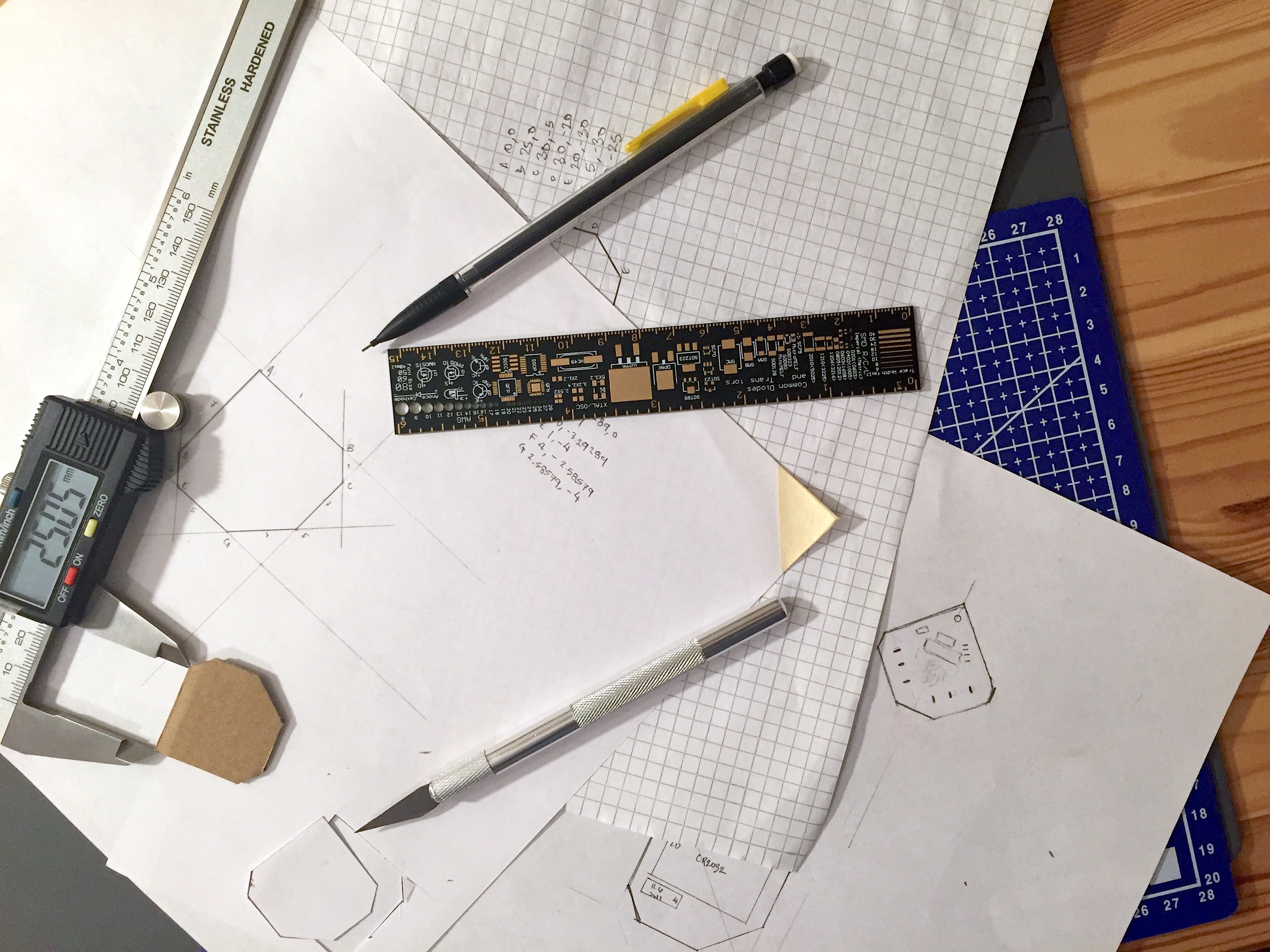
    I originally intended on using Inkscape to design and export a DXF file to specify the edge cuts on the PCB in KiCAD. However, I had a bit of difficulty understanding how to use Inkscape for precise layout. Instead, because my design was a rather simple geometry made up from a series of triangles, I could calculate the coordinates for each point and use KiCAD's coordinate system directly. The strange thing in PCBNew is that the origin is a random point in the upper left, outside of the border of the design space, but I just used that origin (instead of calculating offsets) and then moved the final polygon into the layout space.

  • Initial Parts Selection and Layout

    Thomas Countz04/03/2021 at 20:36 0 comments

    KiCAD Hype.mp4 from Thomas Countz on Vimeo.

    Time to start building footprints and layout in KiCAD. I came up with a seven sided design that I'll upload in the next log. The intention is for the circuit board to be worn as a pendant.

    I'm still waiting on the THT components to arrive from Futurlec so that I can prototype the capacitor and resistor values. Until then, I don't think I'll be ready to order the SMD parts, but because everything will be 0805s, I should be able to order the PCB sooner, rather than later.

  • Simulations

    Thomas Countz03/28/2021 at 18:38 0 comments

    Falstad

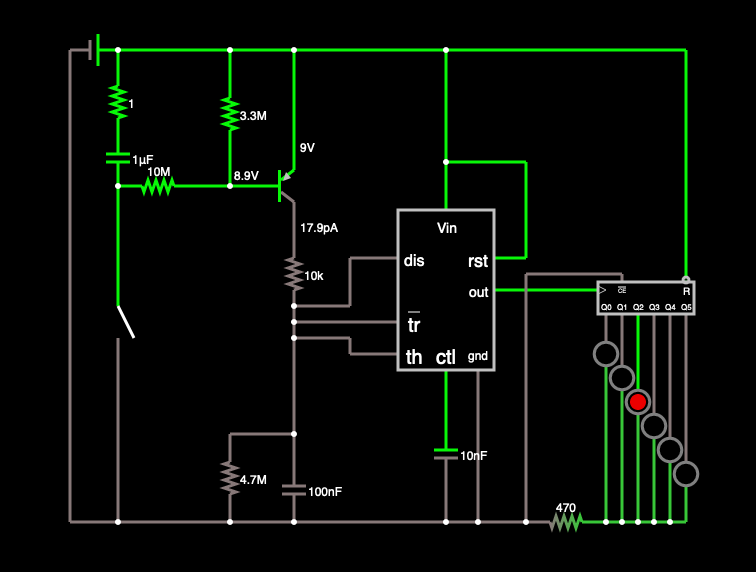
    Run the Falstad simulation here: https://tinyurl.com/yhqfvbpn

    LTspice

    To run the simulation in LTspice, you'll need to download the CD4000.zip file under the project documents and install the model libraries and symbols before downloading and opening hexo.asc

    * /Documents/LTspice/Hexo.asc
    XU1 0 N003 N006 +V NC_01 N003 N003 +V NE555
    V1 +V 0 9
    R1 0 N003 4.7Meg
    C1 N003 0 100n IC=0
    R2 N003 N005 10K
    Q1 N005 N002 +V 0 BC557C
    R3 N002 +V 3.3Meg
    R4 N001 N002 10Meg
    S1 0 N001 N004 0 SW
    V2 N004 0 PULSE(0 1 0.5 0 0 0.1 0 1)
    XU2 0 0 N006 N007 N009 N010 N011 N012 N013 N014 N015 N016 N017 0 VDD 0 CD4017B VDD=3.7 SPEED=1.0 TRIPDT=5e-9
    D1 N007 N008 QTLP690C
    D2 N009 N008 QTLP690C
    D3 N010 N008 QTLP690C
    D4 N011 N008 QTLP690C
    D5 N012 N008 QTLP690C
    D6 N013 N008 QTLP690C
    D7 N014 N008 QTLP690C
    D8 N015 N008 QTLP690C
    D9 N016 N008 QTLP690C
    D10 N017 N008 QTLP690C
    R5 0 N008 4.7Meg
    C3 +V N001 1µ IC=0
    .model D D
    .lib /Library/Application Support/LTspice/lib/cmp/standard.dio
    .model NPN NPN
    .model PNP PNP
    .lib /Library/Application Support/LTspice/lib/cmp/standard.bjt
    .tran 0 15 0
    .model SW SW(Ron=1 Roff=1000G Vt=0.1 Vh=0)
    .include CD4000.lib
    .lib NE555.sub
    .backanno
    .end
    

  • How the 555 Roulette Circuit Works

    Thomas Countz03/28/2021 at 17:54 0 comments

    You can find the PDF version of this schematic under the project's documents.
    When SW1 is closed, C1 quickly charges to VCC (I think there might need to be a current-limiting resistor between C1 and VCC, though maybe SW1 provides this). After C1 is charged, current begins to flow from VCC through both R3 and the Q1's emitter. Because Q1 base voltage is negative w.r.t. the emitter voltage (Q1 base-emitter voltage), the transistor is active forward and current flow through the collector. (It's a PNP).

    Let's continue as if SW1 is still closed. Now that current is flowing through Q1, the 555 begins to oscillate as if it were in astable mode. Charging and discharging C2 to 2/3 and 1/3 VCC respectively and setting pin 3 (output) high and low in kind.

     Pins 2 (trigger) and 6 (threshold) are tied together so that the 555 can continue to "retrigger" itself when C2 is discharged and the voltage reaches 1/3 VCC. In a typical astable configuration, a resistor is placed between pin 7 (discharge) and tied-together pins 6 (threshold) and 2 (trigger). This has the effect of adjusting the duty cycle by altering the charging speed of C2. In this circuit, the duty cycle is manipulated by altering the charging speed of C2 by way of a steadily reducing current through Q1 instead.

    (Note: I believe there should be a decoupling capacitor at pin 5 (control voltage)).

    Now that the 555 is oscillating, pin 3 (output) sends a square wave clock pulse to the 4017 pin 14 (clock). The 4017 is a decade timer and at each rising edge of the clock pulse it will consecutively set each of it's 10 output pins high. Only one pin is high at a time, the other are low. In the case of this circuit, we're only interested in using 6 of the 10  outputs, so we tie pin 5 (Q6), the seventh pin to be set high, to reset which will cause the 4017 to set it's first output (Q0) high instead.

    All of these outputs are used to drive LEDs which whose cathodes are connected to a common current limiting resistor before being tied to ground. These LEDs will continue to be turned on and off consecutively as long as a clock pulse continues to drive pin 14 (clock).

    Let's continue now as if SW1 is opened after being closed. Once SW1 is open, C1 begins to discharge and current continues to flow through VCC and GND by way of Q1. As C1 discharges, however, Q1 base-emitter voltage begins to climb, i.e. the base voltage starts to become less negative w.r.t. the emitter voltage. As this is happening, less current is flowing through Q1 and C2 is taking longer and longer to charge and therefore the clock pulses from pin 3 (output) of the 555 are beginning to slow (the time between clock pulses is increasing). This has the effect of diminishing the speed at which the 4017 is cycling through the LEDs.

    Eventually, Q1's base-emitter voltage reaches the cutoff threshold (~-0.6v) and current stops flowing through Q1. C1 continues to discharge, however, through R3. At this point, whichever LED the 4017 had set to high last, remains lit.

    I'll include a simulation in the next update so that you can see all of this in action with either LTspice or Falstad.


View all 11 project logs

Enjoy this project?

Share

Discussions

Cyril BARBATO wrote 05/04/2024 at 15:33 point

Thanks for you great projet ! But I don't understand where should I place the hexo.asc and CD4017 (.asy) in Kicad to simulate. I can simulate NE555 only but not 4017. Many thanks for your help.

  Are you sure? yes | no

Ken Yap wrote 04/11/2021 at 02:10 point

If that's your real name in your profile, it's evidence of nominative determinism. 😉 Nice project BTW. 👍 Back in the day a dice project of mine filled a cigar box and was mains powered.

  Are you sure? yes | no

Thomas Countz wrote 04/11/2021 at 13:45 point

Thanks! I always knew my last name would Countz for something. 😉 What an awesome ride the world of electronics has gone on. Next thing we know, someone will be working on an electronic die that's embedded in a contact lens and powered by saline. 😆

  Are you sure? yes | no

Similar Projects

Does this project spark your interest?

Become a member to follow this project and never miss any updates