-
New Revision
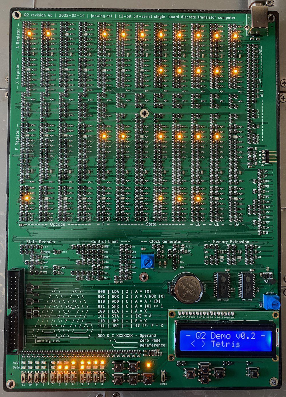
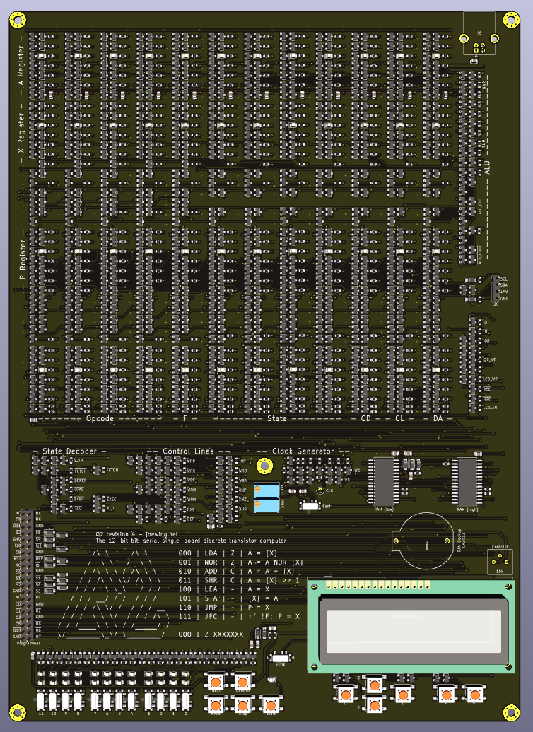
04/03/2022 at 19:44 • 0 commentsI recently ordered a new revision of the Q2:
![]()
Some of the bigger changes since the last version:
- Smaller footprint.
- I2C interface.
- Memory extension.
- New clock generator.
- Green with yellow LEDs.
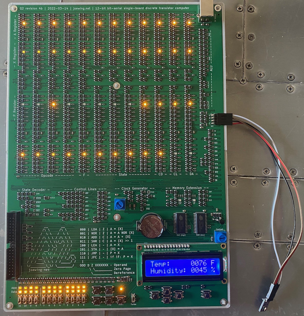
The I2C interface allows the Q2 to communicate with sensors. Here it is showing the temperature and humidity from a SHT31 sensor:
![]()
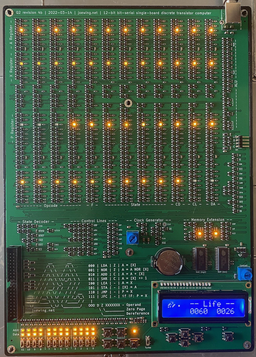
The memory extension allows the Q2 to use double the memory. Here it is simulating Conway's Game of Life in the second field:
![]()
This version is able to run somewhere around 150 kHz before becoming unstable. Note that there is a "turbo" switch which disconnects a capacitor from the oscillator. When the turbo switch is off, the clock runs between ~50 Hz and ~200 Hz. When the turbo switch is "on", it runs between ~50 kHz and ~200 kHz.
The current version has a problem with power-on-reset (power off to be specific), where it corrupts memory when power is disconnected. This is easily fixed by soldering a MCP100 supervisor to the enable pin of the RAM, a change that I plan to incorporate directly into the next revision. Since the RAM itself is implemented with integrated circuits, I don't feel like this is cheating too much and it's a very robust solution.
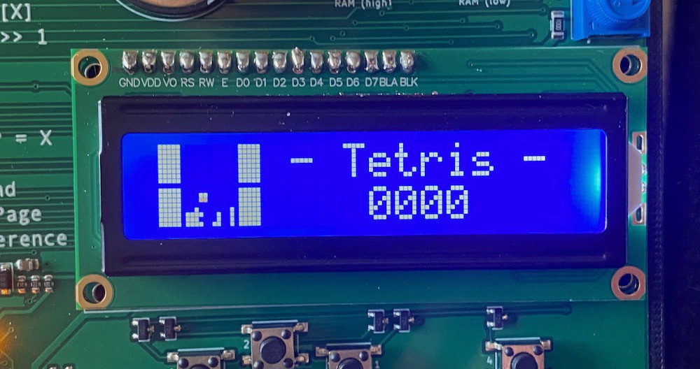
I've also written a few new games for the Q2 including Tetris and Space Invaders. These can be run in the online simulator and the Q2L code available in GitHub. Tetris on a 1602 LCD is a little hard to see, but not impossible:
![]()
-
New PCB Layout
08/07/2021 at 20:35 • 0 commentsIt's been a while, but I finally put together a new layout for the Q2 that uses the new flip-flop design and exposes an I2C interface. Since the new flip-flop design is smaller, the board is also smaller, coming in at 200mm by 278mm, which is about the size of a US letter sheet of paper (for reference, the previous design was 240x314mm). It currently uses 987 transistors. Despite my investigations into making the design faster, I think I'm happy with it as is. Here's a render of the PCB:
![]()
I haven't ordered the board yet since I'm still trying to decide if there are any other changes I want to make. Other I/O options or networking would be especially interesting, though I2C already provides a lot of possibilities for sensors, EEPROM, real-time clocks, etc.
-
Smaller Flip-Flops
05/08/2021 at 18:53 • 0 commentsI started out by looking into RTL as a possible substitute for NMOS for the Q2 as a way to speed it up. In the end, I think NMOS is probably the best bet:
- RTL requires base resistors, which greatly increases component count.
- An RTL gate always draws power (when low, just like NMOS, but also when high, through all output gates). This makes it even more difficult to get a low-power (sub-500mA) design, which is important since I want to be able to run the Q2 off of a USB adapter.
- RTL really only works well with NOR gates, which makes the logic slightly more complex (though in reality, NMOS works better with NOR gates too).
From my experiments, an RTL design can easily go faster, but given the power constraint, it isn't a clear win.
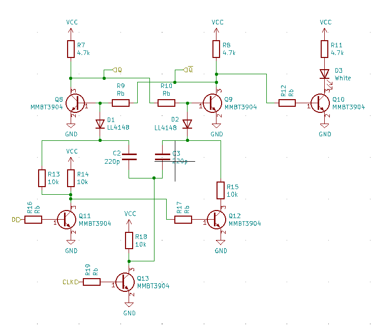
Despite this outcome, the RTL investigation caused me to look into alternative flip-flop designs. Given the 46 flip-flops in Q2, the simple edge-triggered design I had in NMOS wasn't going to cut it in RTL. So I started looking into a pulse-triggered flip-flop (shown below). This design is kind of neat because it uses so few transistors. Unfortunately, it doesn't seem to translate easily into NMOS, and it's somewhat picky about component values as you increase the clock frequency (not to mention the high component count).
![]()
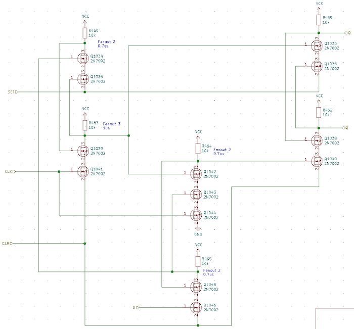
The current Q2 flip-flop design is shown below (without the LED section). It's basically the classic positive-edge triggered flip-flop from NAND gates with set and reset.
![]()
Using 14 transistors, 7 resistors, and 1 LED each, these DFFs make up most of the Q2 by component count and area. So saving even one component would be a good savings.
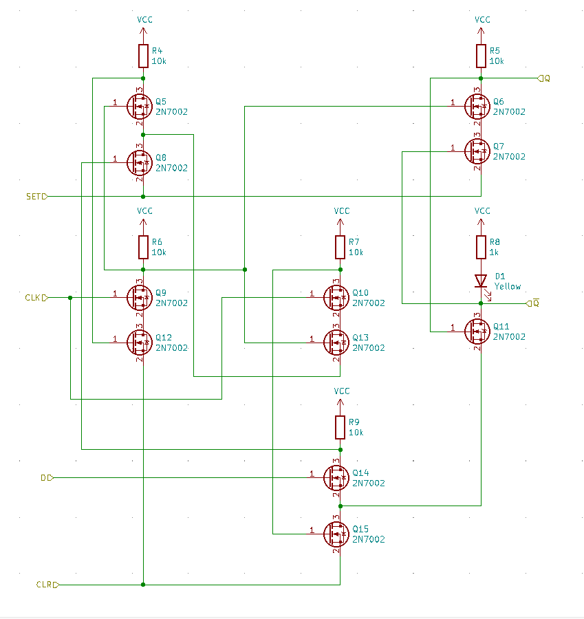
A new design is shown below. By re-arragining some inputs, it's possible to "share" a couple of transistors. Also, by switching to an LED with a low voltage drop, we can save a transistor and resistor, using the LED as part of the pull-up. We're left with a positive-edge triggered D-flip-flop with set and reset, using 11 transistors (all the same type), 6 resistors, and 1 LED.
![]()
The smaller flip-flop design will save 138 transistors and 46 resistors. In addition, the pull-up on the inverted output is actually faster due to the low resistance to power the LED.
-
Transistor Comparison Results
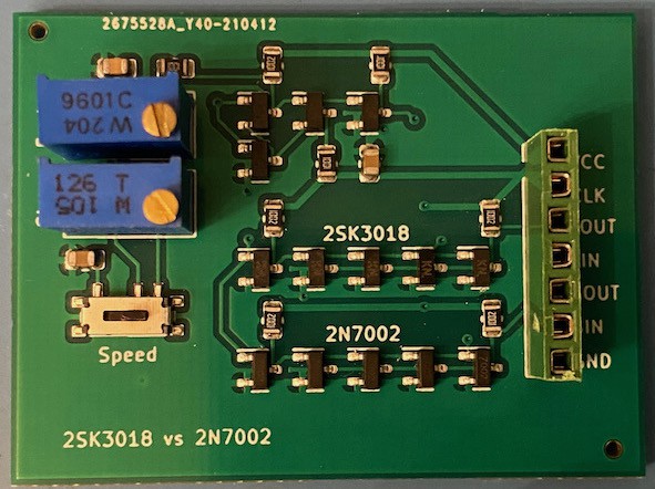
04/24/2021 at 14:51 • 0 commentsFollowing up on my search for faster transistors, I got the boards back earlier this week to test a new candidate transistor (a 2SK3018 vs 2N7002). The good news is that the surface mount switch I wanted to try appears to work just fine. Unfortunately, the new transistor does not appear to improve performance nearly as much as I had hoped.
![]()
For the test, I have the output of an oscillator tied to an inverter implemented with 4 transistors of each type in parallel (I ended up going with a NOR structure instead of a NAND structure). The graph below shows the results.
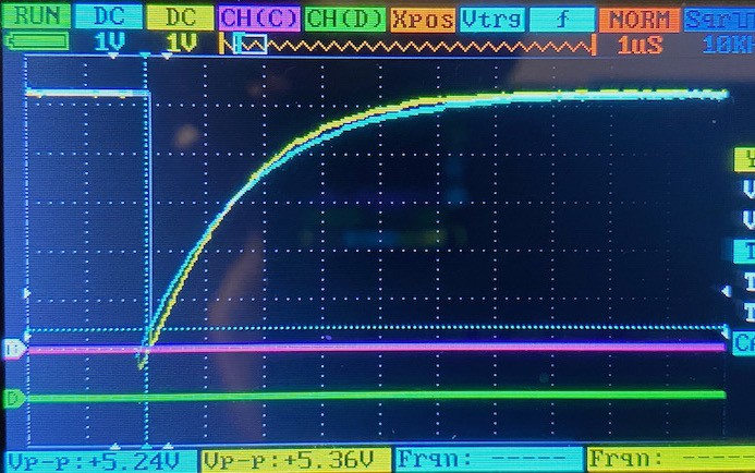
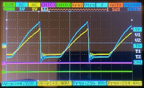
![]()
The blue line is the output fo the 2SK3018 inverter and the yellow line is the output of the 2N7002 inverter. There is maybe some difference, but it's hard to see here.
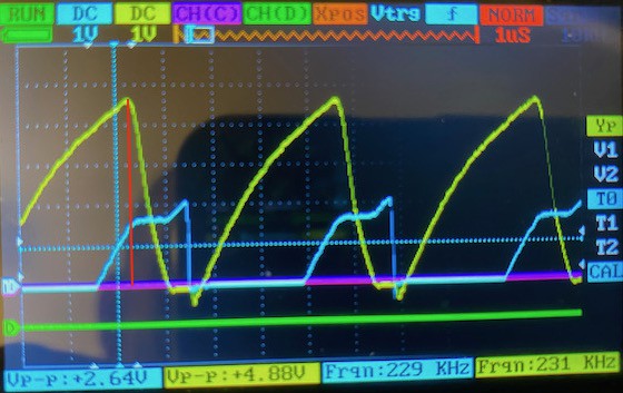
To investigate further, here is the input compared to the output for the 2N7002 inverter:
![]()
The output is in yellow and the input is in blue. The threshold voltage is apparent and seems to be around 1.6V. After somewhere around 1.8us, the input has reached 2V.
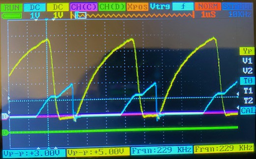
Nothing too surprising. Here's the 2SK3018:
![]()
Again, the output is in yellow and the input is in blue. Here we see a lower threshold voltage of what appears to be 1.2V. Unfortunately, after 1.8us, the input has only reached 2V. This is actually quite similar to the 2N7002.
Looking at the data sheets, although sparse on details, maybe this isn't completely unexpected. For the 2N7002, the maximum capacitance is given as 50pF and no typical capacitance is listed. For the 2SK3018, only a typical capacitance is given as 13pF.
The lower threshold is an advantage, but we need to make sure that external components that the Q2 uses, such as the SRAM and LCD, still get a high enough voltage for the high level. In the end, I'll probably just go with the cheapest transistor for the next revision. Although it would be nice to get some more speed, I would like to be able to do so without adding significantly to the size or power requirements of the Q2.
One, perhaps obvious, observation from this experiment that might speed things up is that in NMOS gates with a lot of inputs are slow. The graph below compares two 4-input NAND gates. For the NAND gate in yellow, the first input is switched (closest to ground). For the NAND gate in blue, the last input is switched (other inputs are held high).
![]()
When the first input is switched the output only reaches 3V after 2.4us whereas when the last output is switched the output reaches 4V. I'm guessing this effect is due to the output capacitance combined with the on-state resistance. For the address decoder, there is a 12-input NAND gate to check for 0xFFF, which is very slow and probably limiting performance. I plan to revisit that with a more appropriate pull-up. This also implies that re-arranging the order of signals into the gate may improve the speed of the gate (slower signals should go near the output side, and faster signals near the ground side). NOR gates don't slow down with increased inputs quite as much as NAND gates, but still slow down as the number of inputs increases almost certainly due to the output capacitance.
-
I2C
04/14/2021 at 02:21 • 0 commentsI should have my test board for the 2SK3018 transistors back next week, but in the meantime I've been thinking about other changes.
In the interest of adding more I/O capabilities, I think I've settled on adding an I2C interface to the Q2. I2C is pretty easy to support, requiring 2 open-drain outputs (SDA for data and SCL for a clock), and an input (only SDA assuming there isn't a need for clock stretching).
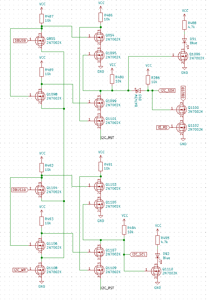
To implement the output for I2C is the most complicated, requiring a latch for SDA and SCL. Input is easy, requiring only a single NAND gate. Here's the current proposal:
![]()
The idea is that bit 11 of address 0xFFF will select between the LCD (0) and I2C (1), allowing easy access to the LCD just as before. When bit 11 is set, bit 10 sets SCL and bit 9 sets SDA. The software for I2C is fairly simple. For start/stop, I think something like this should work:
.def I2C_EN   0x800
.def I2C_SCL  0x400
.def I2C_SDA  0x200

; Note I2C signals are inverted.
i2c_zero:
  .dw   I2C_EN | I2C_SDA | I2C_SCL
i2c_zero_clk:
  .dw   I2C_EN | I2C_SDA
i2c_one:
  .dw   I2C_EN | I2C_SCL
i2c_one_clk:
  .dw   I2C_EN
i2c_input_mask:
  .dw   ~I2C_SDA

; Send I2C start
; Take SDA low while SCL stays high.
i2c_start:
  sta   =x1
  lda   i2c_one_clk   ; SDA=1, CLK=1
  sta   @=neg1
  lda   i2c_zero_clk  ; SDA=0, CLK=1
  sta   @=neg1
  jmp   @=x1

; Send I2C stop
; Take SDA high while SCL stays high.
i2c_stop:
  sta   =x1
  lda   i2c_zero_clk    ; SDA=0, CLK=1
  sta   @=neg1
  lda   i2c_one_clk     ; SDA=1, CLK=1
  sta   @=neg1
  jmp   @=x1
For writing, we just loop over each bit. Being a 12-bit architecture, we have to shift off 4 bits first. So, something like:
; Write byte in x0.
; Destroys x0-x2
i2c_write:
  sta   =x1

  ; Shift out high 4 bits
  lda   =x0
  add   =x0
  sta   =x0   ; x2
  add   =x0
  sta   =x0   ; x4
  add   =x0
  sta   =x0   ; x8
  add   =x0
  sta   =x0   ; x16

  lea   =8
i2c_write_loop:
  add   =neg1
  sta   =x2

  lda   =x0
  add   =x0
  sta   =x0
  jfc   i2c_write_zero

  ; Write 1
  lda   i2c_one
  sta   @=neg1
  lda   i2c_one_clk
  sta   @=neg1
  lda   i2c_one

  jmp   i2c_write_cont
i2c_write_zero:

  ; Write 0
  lda   i2c_zero
  sta   @=neg1
  lda   i2c_zero_clk
  sta   @=neg1
  lda   i2c_zero

i2c_write_cont:
  sta   @=neg1
  lda   =x2
  jfc   i2c_write_loop

  ; Acknowledge
  lda   i2c_one
  sta   @=neg1
  lda   i2c_one_clk
  sta   @=neg1
  lda   i2c_one
  sta   @=neg1

  jmp   @=x1
Reading is similar. From simulation, this would make reading 256 bytes from an EEPROM take somewhere in the neighborhood of 26 seconds at a 80kHz clock. It would be nice to get this faster, but that's plenty fast to use some I2C sensors or a real-time clock, etc.
-
Faster Transistors
04/04/2021 at 22:04 • 0 commentsThe high gate capacitance of the 2N7002 transistors that the Q2 uses prevents it from running much faster than 80 kHz without becoming unstable. This is because, with resistor pull-ups, the charge stored in the gates is pulled high through the resistor, causing slow rise times when a lot of gates are connected together.
Consider the A register in the Q2, which is 12 bits. To clock the A register, 2 transistor gates per bit need to be pulled high. This is a fanout of 24, so a capacitance of 50pF * 24 = 1200pF. The threshold voltage of a 2N7002 is 2.5V worst-case. If we pull this high through a 10k resistor, we get the following expression for the rise time:
Solving for t we get 8.3us for a single gate (if there were only one level of logic, the frequency would be limited to 120 kHz, but there are more levels involved). Substituting a 1k resistor solves the problem, but introduces another: instead of using 0.5mA, we use 5mA. This power draw quickly adds up.The control lines of the Q2 are carefully designed to use 10k resistors where possible, and fall back to 1k in just enough places to allow stable 80 kHz operation. Unfortunately, going faster becomes increasingly difficult and wastes more power. This raises the question of whether another transistor would be more suitable.
We want the following characteristics:
- Low gate capacitance (lower than 50pF)
- Low threshold voltage. Not only does a high threshold cause problems with the supply voltage, it also makes the computer slower since the gate output needs to reach a higher voltage, which takes longer.
- Low price. When using 1000s of transistors, we can't ignore the price.
- ESD protection. Not strictly necessary, but certainly nice to have. With lower gate capacitance, this is probably more important.
One transistor that seems to be a good contender is the 2SK3018 (Shikues brand available through LCSC). It has a gate capacitance of 13pF and threshold of 1.5V. This means that in our example, the delay would be 1.1us with a 10k resistor and 0.11us with a 1k resistor. This should allow running the Q2 at nearly 8x the clock speed and/or save some power.
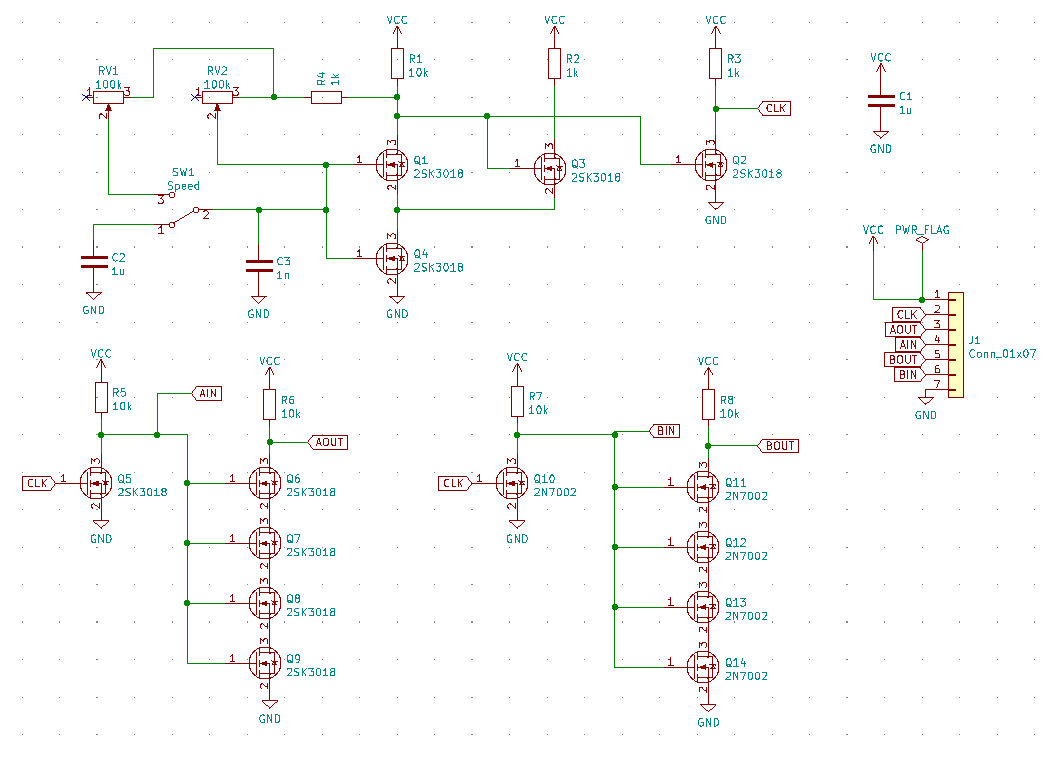
To investigate this further, I put together a simple test circuit. to see how the transistors compare:
![]()
The circuit is a simple relaxation oscillator (identical to the oscillator used in the Q2, but implemented using 2SK3018s instead of 2N7002s). The output is run through two circuits with a fanout of 4 using both types of transistors so I can compare the rise times. This circuit will also allow me to try out an SMD switch so I don't have to worry about soldering switches in future revisions.
 Joe Wingbermuehle