 Yann Guidon / YGDES
The design of the corresponding digital circuit will not make your head spin a lot.
In fact it's almost trivial. There are not enough circuits to hide tricks, though:
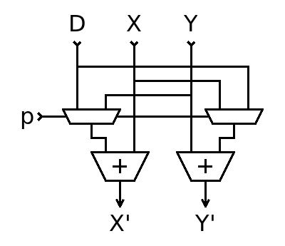
- Just make sure you get the inputs of the two MUXes right.
- The adders are "full size", ie 32 or 64-bits wide, or in fact any size you'd like. You could even reuse "DSP blocks" in a FPGA to optimise the speed.
- The MUX has one input called D, the Data to checksum. Its width is 1/2 the adder's width and the rest is 0-extended. Hence the MUX is one half-size, the other half is plain AND gates.
- Although one cycle only is possible, more cycles will alternate from X to Y and back, as controlled by p, which is a divide-by-to flag.
Apart from that, this circuits is probably as simple as you can get. The critical datapath is one MUX and one ADD so this thing runs FAST.
The "finish" circuit is simple as well :
- Select which variable contains the last computation
- Split the data into its two halves
- Merge them with a XOR
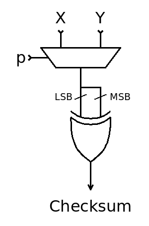
Et voilà.
You get 32 bits if your input word was 32 bits wide.
Ideally, the simplest enhancement that could be done is to "recirculate" the Carry Out from one adder to the Carry Input of the next adder, but apart from x86 (and eventually some POWER cores ?) playing with the carry signals is "a whole different matter".
Discussions
Become a Hackaday.io Member
Create an account to leave a comment. Already have an account? Log In.