 Yann Guidon / YGDES
Going back to the PolarFire FPGA manual (PDF), let's look at the Math Block.
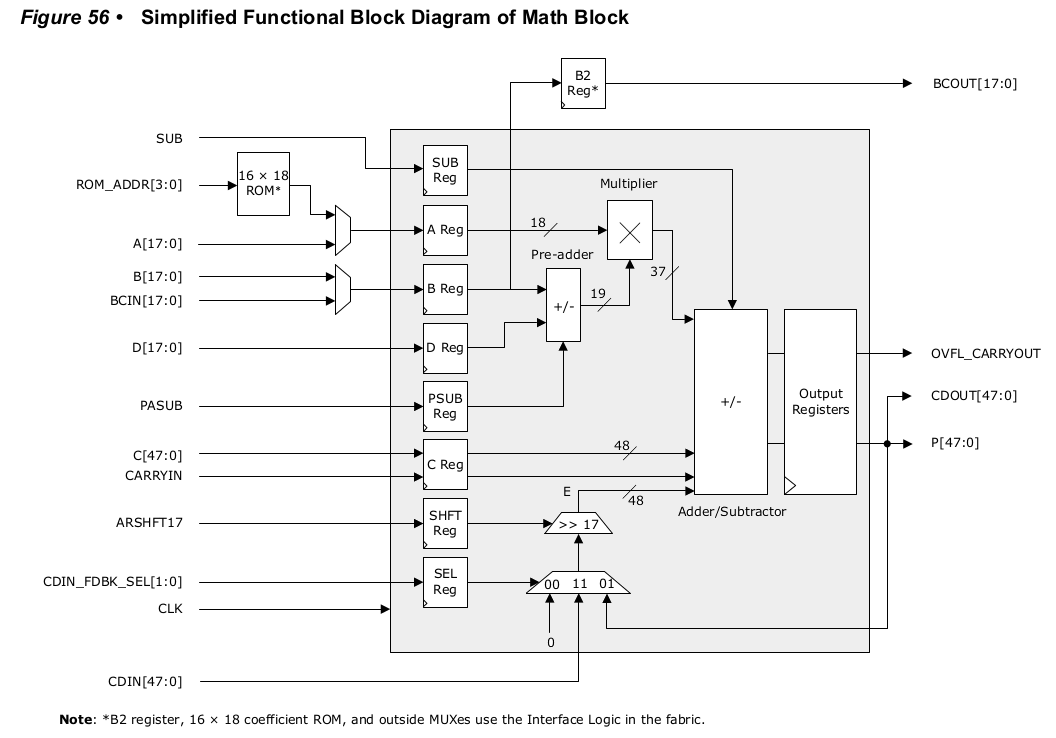
The block can reach 400 MHz though it is not clear under which conditions.
This will not be hard to reach because 6 inputs will be tied to constants so the Pre-adder and the Multiplier sub-blocks will not be active or contribute latency.
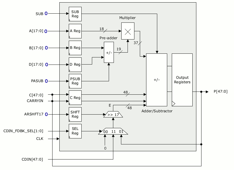
The inputs A[17:0], B[17:0], D[17:0], PASUB, SUB and ARSHIFT17 are tied to 0.
CDOUT[47:0] and OVFL_CARRYOUT are ignored.
This leaves 5 inputs that can be combined to provide one of 3 operations:
- Load
- Keep
- Step
In the original idea,
- C[47:0] is tied to P[47:0] to implement the Y input, with the help of the integrated latches,
- X is created with the internal feedback on the E bus, bypassing the other latches.
- The 3 operation modes are directly controlled by the CDIN_FDBK_SEL[1:0] input, which selects the source of the E operand:
- Load occurs with 11, loading the CDIN bus (the output register must be cleared before)
- Keep occurs with 00 : adding 0 to the accumulator freezes its value
- Step is enabled with 01, adding the delayed Y to the accumulator through the internal feedback path.
But there are two problems:
- There is no direct way to clear the accumulator
- The carry bit can not be tweaked in the feedback path
...
While the first problem can be solved by a MUX on C[47:0], the second is a big setback.
Discussions
Become a Hackaday.io Member
Create an account to leave a comment. Already have an account? Log In.