-
PIMD V2
11/26/2021 at 09:20 • 1 commentPIMD V2
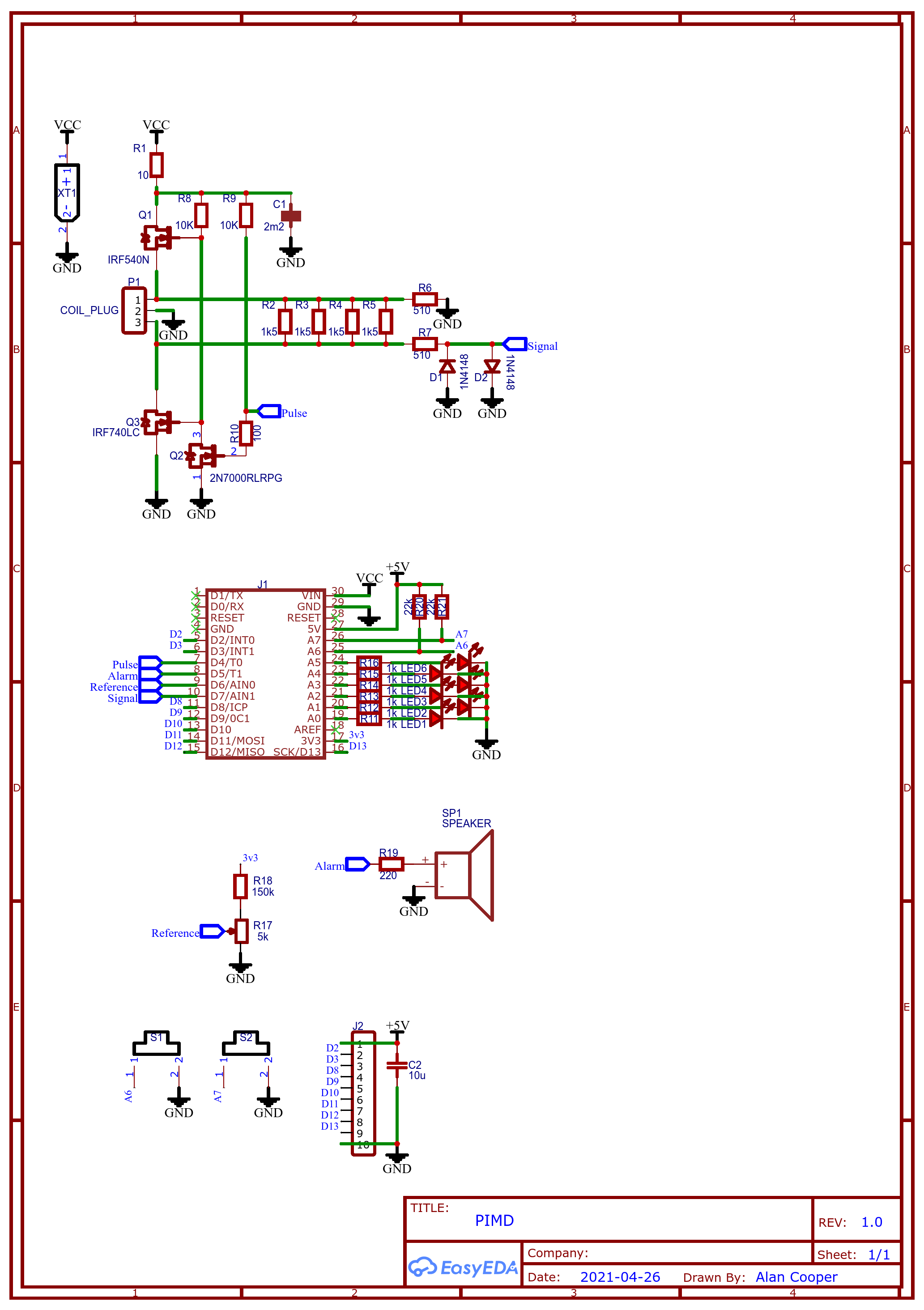
Reworked the schematic to add an OpAmp (OPA2365).
Added A0 to the signal output so I can look alternative signal processing options.
This board uses an IRL540 instead of an IRF540, which reduces the MOSFET voltage drop.
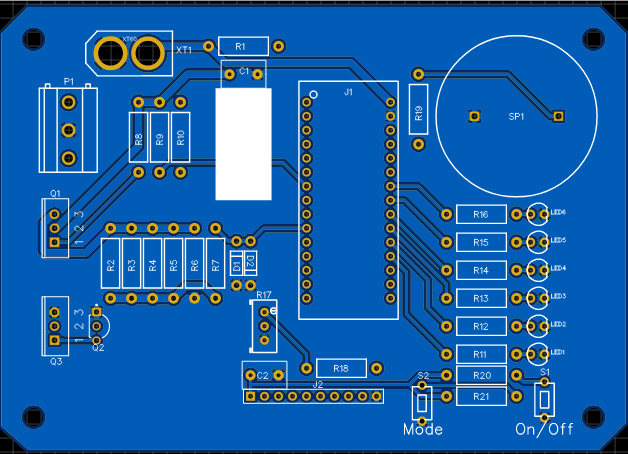
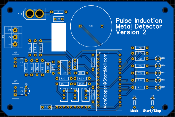
Here is the assembled board before testing:
![]()
Two Signal Processing Approaches
ADC
First we could go the ADC route, the board is setup for this.
With a 1MHz clock, we can do samples every 13 to 14 us without losing accuracy.
We can trade faster conversion for accuracy.
Timer
The current approach measures the time the signal takes to decay to a specific test voltage (~40mV).
We could expand the number of voltage tests by controlling the reference voltage using a R-2R resistor ladder. Unfortunately I did not make provision for this with this board.
TBC ...
AlanX -
Update after a long break
11/10/2021 at 06:19 • 0 commentsAdding Gain
Why do we want to add gain?
In order to increase detection limits we need to increasing the signal to noise ratio (SNR) of the target response. The SNR can be improved by waiting for the coil and ground response to decay.
This works because the target response (for medium to large objects) has a longer time period (decays more slowly). We cannot wait too long or the target signal will be swapped by the noise floor (about 1-2uV).
In general the larger the target the longer the decay time and the longer the time for the optimal SNR measurement.
Therefore, different setting would optimise for small, medium and large objects.
Attempting to filter the coil and ground response would be better for small objects.
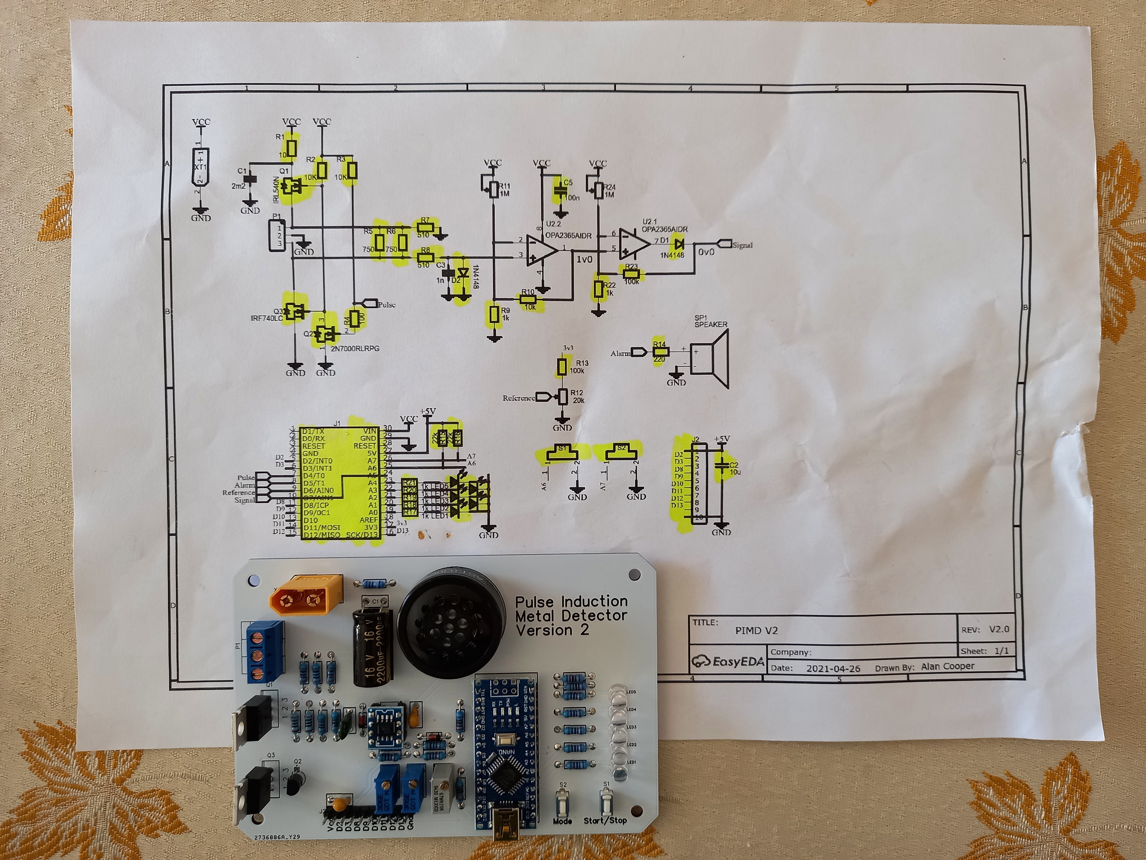
Version 2 - PIMD
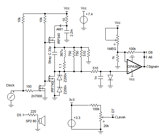
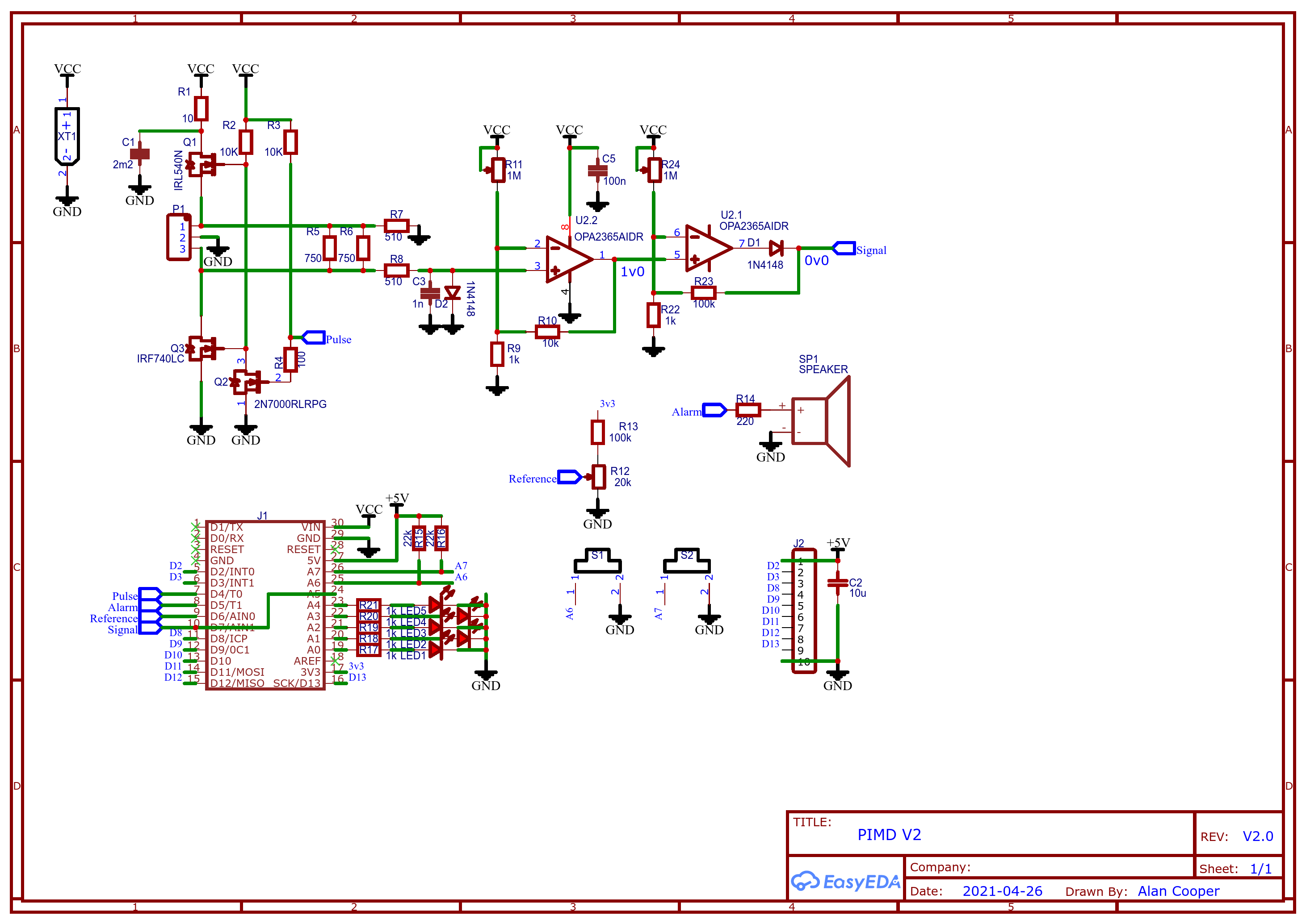
Here is my updated schematic:
![]()
And the PCB:
![]()
Note: I have routed the signal to both D7/AIN1 (the comparator negative input) and A5 (an analog input). This allows experimentation with Analog to Digital systems.
Filtering the Coil and Ground Signal.
PIMD Version 1 code cancels the coil and ground signal by subtracting an exponentially smoothed long time constant filter from an exponentially smoothed short time constant filter. Basically hold the coil on the ground until the signal decays away. Now it only responses to changes in the signal (dynamically). It works but we could do better.
It would be nice to give a signal that indicates that the signal curve/shape has changed.
This can be done with the following code:
- Signal=(G0-S0)+(G2-S2)-4*(G1-S1)
- where G0, G1 and G2 are exponentially smoother long term filter values for different sample points.
- and S0, S1 and S2 are exponentially smoother short term filter values for the same "different" sample points.
This works for three voltage or three timer readings, and the formula can be adapted for more than 3 sample points.
AlanX
-
A Toy PIMD
05/23/2021 at 04:48 • 0 commentsA Toy PIMD
I would describe this PIMD as a "toy". Why? Because it is necessary to detect the target signal immediately after the coil signal has decayed below the target signal, and before the target signal has decayed below the 40 mV threshold. In the field, the ground response will mask the target signal at this point of time.
Corbyn's paper describes the ground response of iron rich lateritic soils as:
- g(t) = (1-P)*exp(-t/T1) + P*exp(-t/T2)
where:
- P = 0.08 to 0.30
- T1 = 75us
- T2 = 550us to 800us
He also presents an estimate for a target response (i.e. decay time constant):
- T = 1.8*D^2
where:
- D is the diameter (m) of the target
For a 1 cm target the estimate for T is:
- 180 us
For a 5 cm target:
- 4.5 ms
The above target decay time constants indicate that detecting targets less than 2.5 cm in diameter will be difficult in iron rich lateritic soils.
Detection Strategies
For large targets (>=5 cm), one strategy is to wait for the ground response to decay well below the target response. For example, if we have an initial 100 mV ground response and a 10 mV target response, then we could wait 4200 us when the ground response is 40 uV and the target response is still 400 uV. Assuming a 10 to 1 signal to noise ratio is desirable.
If we can filter out 90% of the ground response then we only need to wait 520 us for the same 10 to 1 signal to noise ratio.
In either case we need more gain to allow signal sampling much later in the pulse cycle.
Low Pass Input Filter
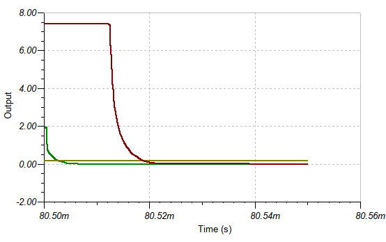
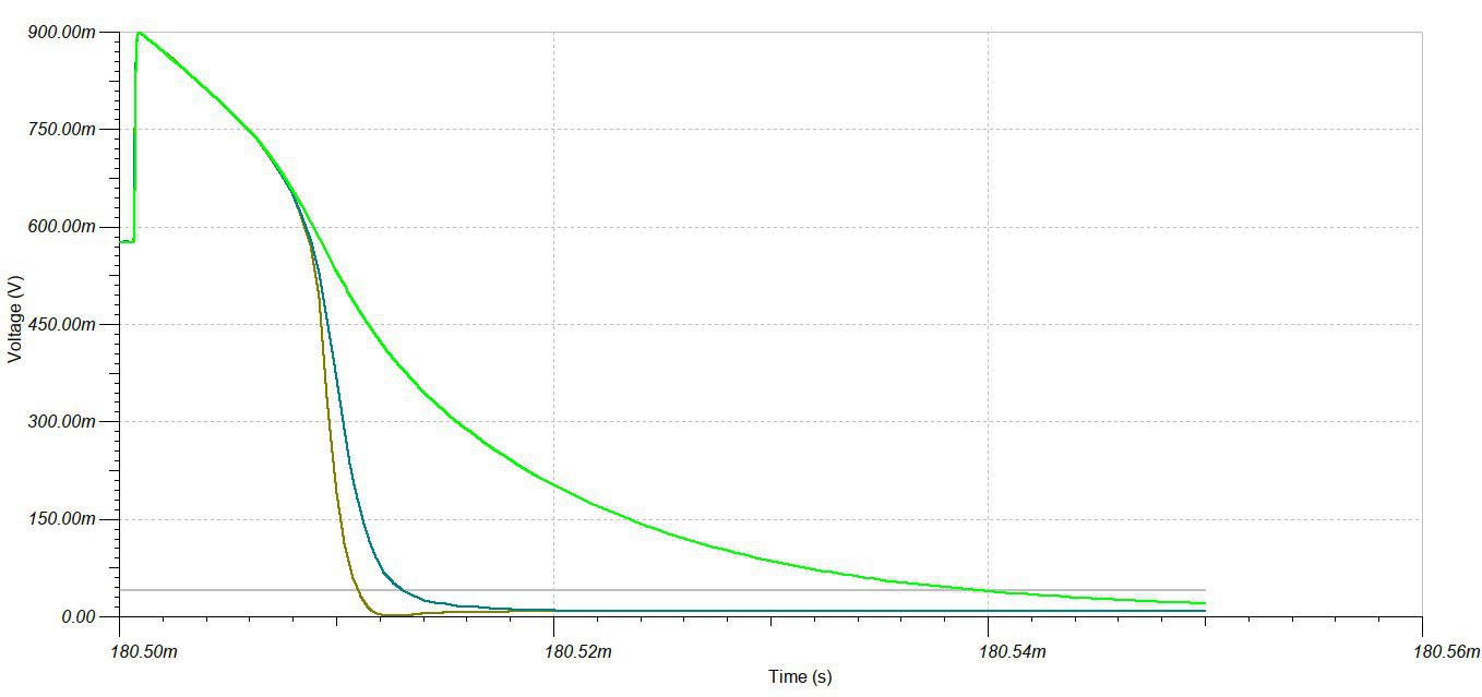
I added a 1nF capacitor (blue curve) to signal input (brown curve). This has minimal impact on the signal but filters out any RF above 100kHz. For a 10kHz low pass filter (green curve) the capacitor would be 10nF but it materially delays the decay of the coil signal.
![]() Noise Floor
Noise FloorThe noise level of the analog comparator is not disclosed in the ATMEGA328 data-sheet but if I use a 741 OpAmp as a model (23nV/sqrt(Hz)), the noise floor for a 100kHz bandwidth and 1k source resistance, will be about 7 uV.
Reducing the bandwidth to say 10kHz would reduce the noise floor to 2.3uV. At the moment the noise floor is not important.
Adding Gain
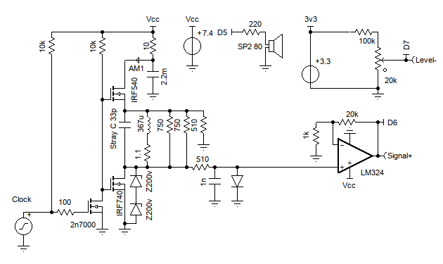
I don't want to use a split power supply OpAmp to avoid the extra power supply. So let have have a look at the LM324:
![]()
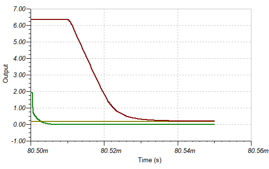
Note: the LM324 is DC coupled and has a gain of x20:
![]()
What you can see here is that the slew rate of the LM324 is far too low (the straight line descending slope) to follow the signal. This is not too surprising as the GBW of the LM324 is 1.2 MHZ and the slew rate just 0.5v/us.
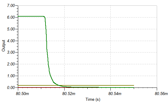
Compare this with the LM3900 Norton OpAmp with a gain of x50:
![]()
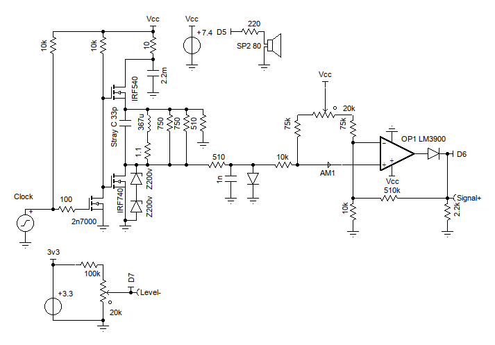
The LM3900 has a 4 MHz GBW and a 20v/us negative slew. But this is about as much gain as you can get with this OpAmp. Here is the lm3900 schematic:![]()
Note the common mode biasing using the 2x75k ohm and 20k Ohm trimmer. The common mode biasing ensures that the OpAmp has sufficient biasing to the inputs to operate correctly. It was a rather tricky design process to work this out.
The output diode drops the output offset from ~200 mV to 0 mV.
Another option is to use a CA3130, it has a slew rate between 10 and 30 v/us and a GBW of 15 MHz. For more gain (per stage), a more modern OpAmp such as the OPA365 is required:
![]()
This OpAmp is rated at a GBW of 50 MHz and a slew of 25 v/uv:
![]()
Note the OPA365 was configured for a gain of x100 but higher gains are possible (x500 per stage).
Pseudo Gain Control
For signal processing it would be nice adjust the signal gain to normalising (i.e. make the start of the the signal the same voltage). This makes removing the ground response (i.e. subtracting the reference signal) more efficient.
While not ideal, we can initially set the analog comparator to the internal 1.25v reference. Start the signal timer at that point, and then measure the time for the signal to decay to the external analog comparator voltage reference (e.i. 40 mv). It is not the same as normalising the signal as there is a time shift but I suspect it will work okay in practice.
Digital Signal Processing (DSP)
I am near the end of what can be done with the analog input comparator. For the next PCB board I will connect the signal input to A5 as well as D6. Then I can explore ADC options and more advance DSP.
New PCB
So I am ready to design a new PCB.
AlanX
-
Test Run
05/22/2021 at 05:41 • 0 commentsTest Run
I assembled the board, made a simple coil and powered up the Nano without the coil power supply. Some edits to the code but otherwise it appears to be working.
Connected the Coil power supply and amazingly it worked. Some tweaks to the exponential filter constants and it detects small coins within half a coil diameter and large coins at about one coil diameter. About as good as similar (honest) detectors on the Internet.
On the Internet I have seen a demonstration of a PIMD discriminating (not responding to) aluminum foil. This is not real, the detector is just rejecting strong and good conducting targets. Easy to do but does not make a good metal detector.
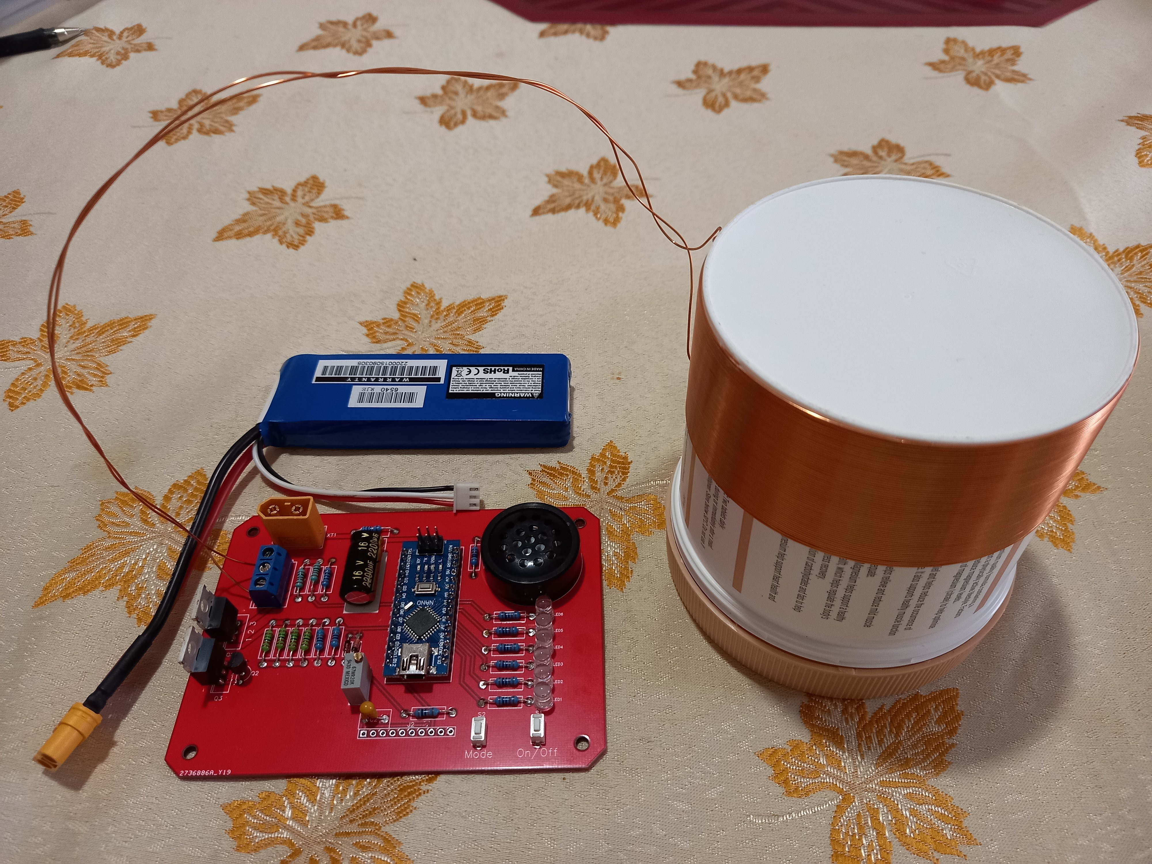
Hers is the setup:
![]()
And the Code:
/* Arduino Pulse Induction Metal Detector */

// Pin definitions
#define pulsePin            4                        // For coil MOSFET gates
#define beepPin             5                        // Buzzer pin
#define compPlus            6                        // Plus (signal) comparator input pin
#define compMinus           7                        // Minus (level) comparator input pin
#define ledPin0            A0                        // Log bar LED0
#define ledPin1            A1                        // Log bar LED1
#define ledPin2            A2                        // Log bar LED2
#define ledPin3            A3                        // Log bar LED3
#define ledPin4            A4                        // Log bar LED4
#define ledPin5            A5                        // Log bar LED5

// Fast versions of digitalWrite(Pin,HIGH); and digitalWrite(Pin,LOW); for all pins on UNO/Nano
#define fastHighPin(Pin) if ((Pin)<8) PORTD|=1<<(Pin); else if ((Pin)<14) PORTB|=1<<(Pin)-8; else if ((Pin)<20) PORTC|=1<<(Pin)-14;
#define fastLowPin(Pin) if ((Pin)<8) PORTD&=~(1<<(Pin)); else if ((Pin)<14) PORTB&=~(1<<(Pin)-8); else if ((Pin)<20) PORTC&=~(1<<(Pin)-14);

volatile unsigned int Magic0=0;
volatile unsigned int Phase0=0;
ISR(TIMER0_COMPB_vect) {
  Phase0+=Magic0;
  if (Phase0<0x8000) {
    fastLowPin(beepPin);
  } else {
    fastHighPin(beepPin);
  }
}

void setup() {
  // Set up pulse pin first - Note: Electronics logic is inverted
  digitalWrite(pulsePin,HIGH);
  pinMode(pulsePin,OUTPUT);
  // Set up comparator inuts
  pinMode(compPlus,INPUT);
  pinMode(compMinus,INPUT);
  // Set up Beeper
  pinMode(beepPin,OUTPUT);
  digitalWrite(beepPin,LOW);
  // Set up Config LED
  pinMode(LED_BUILTIN,OUTPUT);
  // Set up LED bar display
  pinMode(ledPin0,OUTPUT);
  pinMode(ledPin1,OUTPUT);
  pinMode(ledPin2,OUTPUT);
  pinMode(ledPin3,OUTPUT);
  pinMode(ledPin4,OUTPUT);
  pinMode(ledPin5,OUTPUT);
  // Clear LEDs
  digitalWrite(LED_BUILTIN,LOW);
  digitalWrite(ledPin0,LOW);
  digitalWrite(ledPin1,LOW);
  digitalWrite(ledPin2,LOW);
  digitalWrite(ledPin3,LOW);
  digitalWrite(ledPin4,LOW);
  digitalWrite(ledPin5,LOW);

  // No interrupts (just read the ACO bit)
  ACSR=0x00;

  // Reset timer 1
  TIMSK1=0x00;                                       // Disable all timer interrupts
  TCCR1A=0x00;                                       // Normal (just count up and roll over) Config
  TCCR1B=0x00;                                       // Stop timer

  // Piggy back tone to timer0
  OCR0B=0x80;                                        // Trigger interrupt away from millis() interrupt
  TIMSK0|=(1<<OCIE0B);                               // Enable Timer0 Compare B interrupt

  // Set Serial - for debug
  // delay(100);
  // Serial.begin(9600);
  // while (!Serial);
  // delay(100);

}

void loop() {
  // PIMD constants

  // Repetition rate
  unsigned long previousMillis=0;
  unsigned long currentMillis;
  unsigned long intervalMillis=20;

  // Coil pulse timing
  unsigned long pulseTime=500;                       // Coil on time (us)
  unsigned long startMicros;
  unsigned long endMicros;

  // Signal processing
  unsigned long decayTime;                           // The Signal
  unsigned long refExpFilter=0;                      // Reference exponential filter
  unsigned long sigExpFilter=0;                      // Signal exponential filter
  unsigned long refTest;                             // Reference (smoothed) test value
  unsigned long sigTest;                             // Signal (smoothed) test value
  unsigned int refFilterConst=9;                     // Exponential filter time power constant (setting time about 60 seconds)
  unsigned int sigFilterConst=3;                     // Exponential filter response time: lower is faster but more noisy
  unsigned int thresholdConst=1;                     // Sensitivity

  // Beeper frequency
  unsigned int magicNum=0;                           // magicNum=Freq*67.108864;

  // Stop tone and set beepPin LOW
  Magic0=0;
  Phase0=0;

  // Clear configuration
  bool configState=true;
  unsigned int Config=0;                             // Config flag {0|1-6}

  // Get configuration before start
  bool Start=false;                                  // Start flag {false|true}

  // Clear Config and bar display LEDs
  digitalWrite(LED_BUILTIN,LOW);
  digitalWrite(ledPin0,LOW);
  digitalWrite(ledPin1,LOW);
  digitalWrite(ledPin2,LOW);
  digitalWrite(ledPin3,LOW);
  digitalWrite(ledPin4,LOW);
  digitalWrite(ledPin5,LOW);

  // Get configuration
  while (configState) {
    // Set Config (A7) before turning on power
    while (analogRead(A7)<=511) {                    // While button pushed
      Config=Config%6;
      Config++;
      digitalWrite(ledPin0,LOW);
      digitalWrite(ledPin1,LOW);
      digitalWrite(ledPin2,LOW);
      digitalWrite(ledPin3,LOW);
      digitalWrite(ledPin4,LOW);
      digitalWrite(ledPin5,LOW);
      if (Config==1) {
        magicNum=16384;                              // 244Hz (freq*67.108864)
        refFilterConst=9;                            // Setting time about 60 seconds
        sigFilterConst=3;                            // Response time (medium)
        thresholdConst=1;                            // Sensitivity (high)
        digitalWrite(ledPin0,HIGH);
      }
      if (Config==2) {
        magicNum=0;                                  // 0Hz (off)
        refFilterConst=9;                            // Setting time about 60 seconds
        sigFilterConst=3;                            // Response time (medium)
        thresholdConst=1;                            // Sensitivity (high)
        digitalWrite(ledPin1,HIGH);
      }
      if (Config==3) {
        magicNum=16384;                              // 244 Hz;
        refFilterConst=8;                            // Setting time about 30 seconds
        sigFilterConst=3;                            // Response time (medium)
        thresholdConst=1;                            // Sensitivity (high)
        digitalWrite(ledPin2,HIGH);
      }
      if (Config==4) {
        magicNum=16384;                              // 244 Hz;
        refFilterConst=7;                            // Setting time about 15 seconds
        sigFilterConst=2;                            // Response time (fast)
        thresholdConst=1;                            // Sensitivity (high)
        digitalWrite(ledPin3,HIGH);
      }
      if (Config==5) {
        magicNum=0;                                  // 0Hz (off)
        refFilterConst=9;                            // Setting time about 60 seconds
        sigFilterConst=3;                            // Response time (medium)
        thresholdConst=1;                            // Sensitivity (high)
        digitalWrite(ledPin4,HIGH);
      }
      if (Config==6) {
        magicNum=0;                                  // 0Hz (off)
        refFilterConst=9;                            // Setting time about 60 seconds
        sigFilterConst=3;                            // Response time (medium)
        thresholdConst=1;                            // Sensitivity (high)
        digitalWrite(ledPin5,HIGH);
      }
      delay(500);
    }
    // Use power on to exit config
    while (analogRead(A6)<=511) {                    // If exit config state
      while (analogRead(A6)<=511);                   // Wait for buton release
      delay(20);                                     // Wait for debounce
      configState=false;                             // Set exit config state
    }
  }

  Start=true;
  while (Start) {
    // Set up 20ms cycle
    currentMillis=millis();
    if (currentMillis-previousMillis>=intervalMillis) {
      previousMillis=currentMillis;

      // Pulse the coil - Note: Electronics logic is inverted
      fastLowPin(pulsePin);
      delayMicroseconds(pulseTime);
      fastHighPin(pulsePin);

      // Measure coil decay time (after coil turned off)
      TCCR1B=0x01;                                   // Start timer 1 (16 MHz clock)
      while (~ACSR&0x20);                            // Wait for comparator to trip
      TCCR1B=0x00;                                   // Stop timer 1
      decayTime=TCNT1;                               // Read timer 1
      TCNT1=0;                                       // Reset timer 1

      // Update reference exponential filter
      refExpFilter=refExpFilter-(refExpFilter>>refFilterConst)+decayTime;

      // Update signal exponential filter
      sigExpFilter=sigExpFilter-(sigExpFilter>>sigFilterConst)+decayTime;

      // Set LED and tone on if signal detected
      refTest=(refExpFilter>>refFilterConst);
      sigTest=(sigExpFilter>>sigFilterConst);
      if (sigTest>refTest) {
        sigTest=(sigTest-refTest)>>thresholdConst;
      } else {
        sigTest=0;                                   // No signal "reset"
      }
      // Turn off display
      digitalWrite(ledPin0,LOW);
      digitalWrite(ledPin1,LOW);
      digitalWrite(ledPin2,LOW);
      digitalWrite(ledPin3,LOW);
      digitalWrite(ledPin4,LOW);
      digitalWrite(ledPin5,LOW);
      if (sigTest>0) {
        // Generate log bar display
        digitalWrite(ledPin0,HIGH);
        if (sigTest>>=1) digitalWrite(ledPin1,HIGH);
        if (sigTest>>=1) digitalWrite(ledPin2,HIGH);
        if (sigTest>>=1) digitalWrite(ledPin3,HIGH);
        if (sigTest>>=1) digitalWrite(ledPin4,HIGH);
        if (sigTest>>=1) digitalWrite(ledPin5,HIGH);
        // Start tone
        Magic0=magicNum;
      } else {
        // Stop tone and set beepPin LOW
        Magic0=0;
        Phase0=0;
      }
    }

    // Check for power down and restart loop();
    if (analogRead(A6)<=511) {
      while (analogRead(A6)<=511);                   // Wait for buton release
      delay(20);                                     // Wait for debounce
      Start=false;                                   // Set flag off
    }
  }
}
Receive Signals
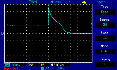
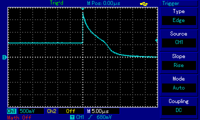
Here is the no target receive signal:
![]()
It approximates the simulation with the exception of the diodes 1.6v rather than 0.9v.
The signal falls to the threshold voltage (i.e. 40mV) after about 14 us.
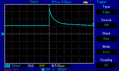
Here is a small target response:
![]()
The signal falls to the threshold voltage after about 20 us.
And here is a (very) large target response:
![]()
The pulse cycle will wait until the signal decays to the threshold, but after 8 ms the results will be meaningless.
Improvements
The first improvement was to lower the threshold voltage to 30mV to increase the sensitivity to small targets. The optimal threshold voltage will depend on the picked up noise level and usability. Its the old problem of detecting a uV signal on top of mV noise.
The main problem that I see is that the exponential smoothing/filtering works but would be better before the analog comparator. Perhaps a higher order low pass filter to remove as much of the no target signal as possible before the analog comparator and the exponential filter post the analog comparator.
AlanX
-
Modelling the Flip Coil
05/07/2021 at 06:20 • 1 commentModelling the Flip Coil
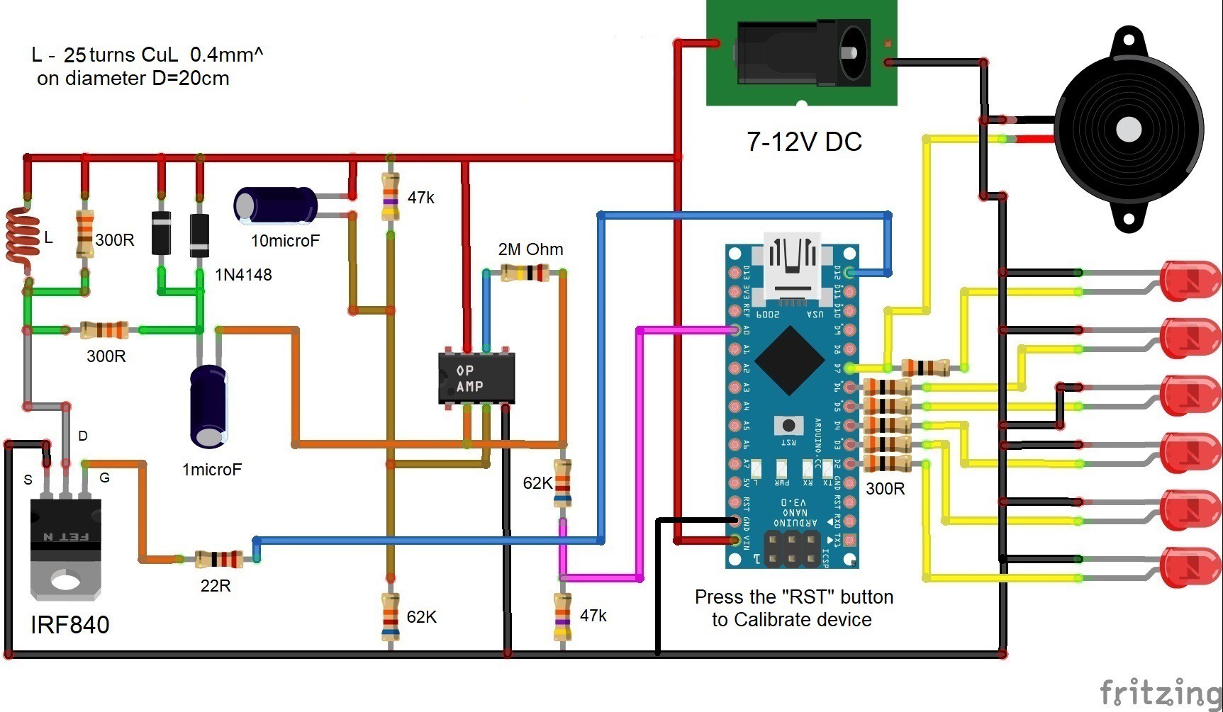
Here is a schematic based on Mirko Pavleski's Pulse Induction Metal Detector (PIMD) (https://hackaday.io/project/176291-diy-simple-sensitive-arduino-metal-detector):
![]()
(Note: I think the 62k/47k output resistor divider should be moved from the inverter input of the op-amp to the output of the op-amp?).
Mirko's design really appeals to me because of its simplicity.
The main problem I see is that power supply is not isolated from the inductive voltage spikes from the coil. It would work with a low internal resistance battery but an electronic power supply could be a problem. There is a risk that the inductive voltage spike could be upset and/or damage the op-amp and/or the Nano.
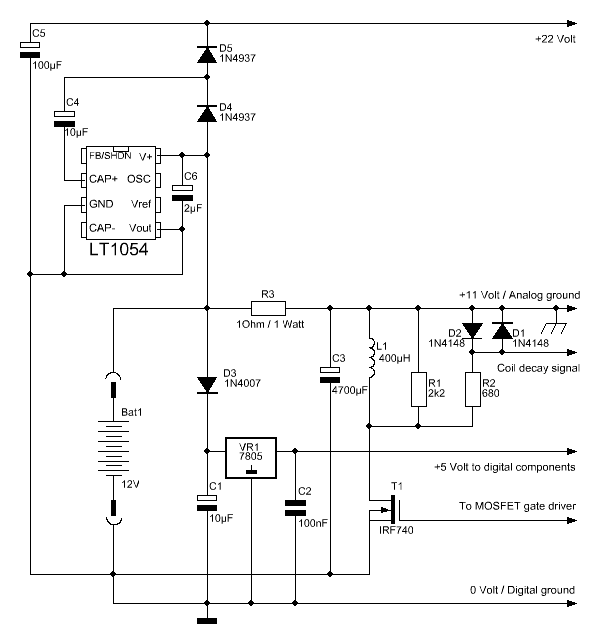
Here is Lammert Bies' PIMD (https://www.lammertbies.nl/electronics/pi-metal-detector):
![]()
My favourite however, is the "Flip Coil" by JorBi (https://www.instructables.com/Arduino-Based-Pulse-Induction-Detector/):
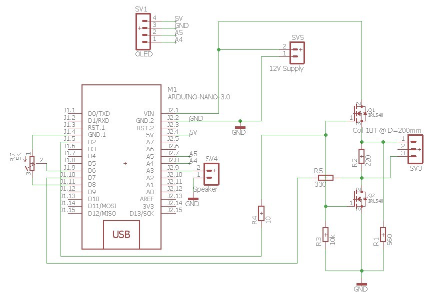
![]()
Here he uses R1 to ground the negative inductive voltage side of the coil during the receive period. He also isolates the coil by switching off both MOSFETs during the receive period. This is very clever!
He also uses the ATMega's analog comparator to time the decay of the signal to reference voltage (40mV). Rather than the analog to digital converter (ADC). Again, a very clever solution.
Some notes/faults with his design are:
- No protective diodes for the Nano (he relies on the Nano's internal diodes).
- No power supply decoupling. Risk of inductive voltage spikes upsetting the Nano.
- MOSFET Q2 should have a higher breakdown voltage to shorten the coil current decay. I would use an IRL740 (400v) or an IRL840 (600v) or equivalent. MOSFET Q2 has to be an IRLXXX type in order to be directly driven by the Nano.
- MOSFET Q1 really does need to be an IRLxxx version to minimize the voltage drop across the MOSFET.
- Rather than use D8 to power the reference voltage potentiometer he should used the Nano 3v3 voltage supply.
- The speaker line should include a 220R current limit resistor.
- The I2C lines should have 4k7 pull up resistors.
MOSFET Types
As I was researching this project it took a while to realize that there are "normal" MOSFETs (i.e. IRF540) with a gate threshold between 2 and 4 volts (read 4 volts) and "logic" MOSFETs (i.e. IRL540) with a gate threshold between 1 and 2 volts (read 2 volts).
In my case I used an IRF540 and an IRF740 until I realized benefit of using the IRLxxx series for this application. Unfortunately I had already sent of a PCB for manufacture.
![]()
- A direct XT connection on the PCB for 7.4v or 11.1v rechargeable LiPo battery packs.
- A logarithmic LED display.
- Not immediately obvious are two switches that use the often unused A6 and A7 pins of the Nano. To use these pins, an analogRead() is required:
// Check for power down and restart loop();
if (analogRead(A6)<=511) {
while (analogRead(A6)<=511); // Wait for buton release
delay(20); // Wait for debounce
Start=false; // Set flag off
}- I have used four resistors (1k5) in parallel to increase the power dissipation.
- Because I am using the IRFxxx series MOSFETs I have to drive the power MOSFET gates from the high voltage (>5v) supply. Thus the 2N7000 MOSFET gate driver.
- The gate driver requires an inverted logic from the Nano (i.e. normally high (off), pulse low (on)).
- One of the switches (i.e. On/Off) will be used to power down the Nano rather than disconnect the power supply.
- The other switch (e.i. Mode) will be used to toggle between to configurations.
My PCB Layout
Here is the board I sent off to be made:
![]()
Modelling the Schematic
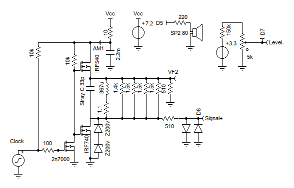
I used TINA to model the schematic:![]()
The spice models have limitations, one being the MOSFET breakdown voltage, thus the two series zeners across the IRF740.
The schematic has been optimized to determine the resistor values for critical damping of the signal.
Checking the voltage drop over the power MOSFETs indicated that the IRF540 needs to be upgraded to an IRL540 type. The voltage drop across the IRF540 was about 4 volts, while the voltage drop across the IRL540 would be about 2 volts.
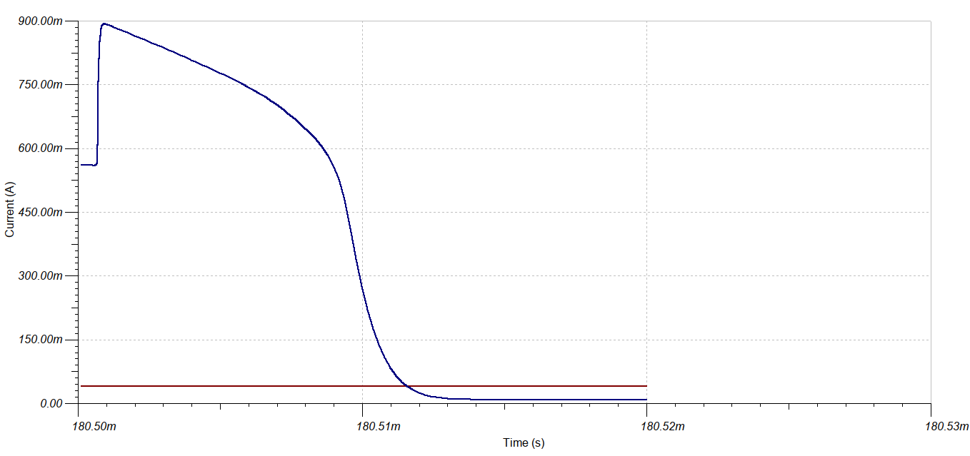
Here is the modelled receive signal (coil voltage decay only):
![]()
The graph shows a critically damped signal (blue) and the 40mv threshold (red). The initial jump up just after 180.500 ms is the coil pulse being switched off and limited by the protection diodes. The modelling suggest that the coil voltage decay will be practically zero after 14 us.
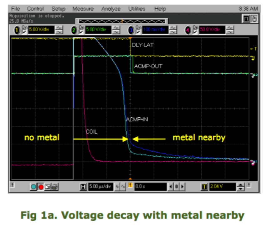
The Target Signal
What does the target signal look like? This image is from Jozef Froniewski of Silego Technology
![]()
Note that the "no metal" curve maps reasonably with my modelled curve.
Ground Effect
Although Corbyn in his March 1980 Wireless World paper states he had not found any gold with his PIMD, he did find several nuggets up to 1 oz in size by 1981.
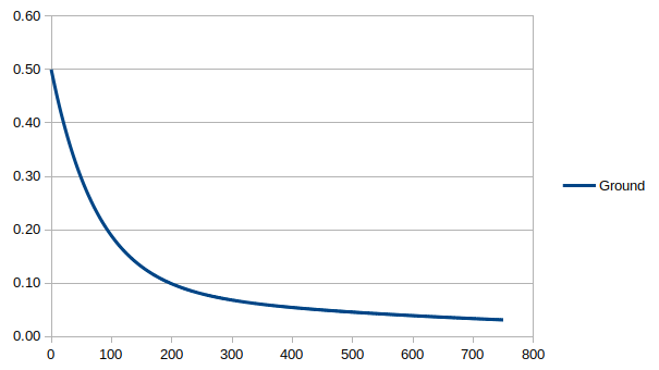
His design looked at removing the "ground effect" of the iron rich lateritic soils of the Eastern Goldfields of Western Australia. He modelled the ground response as:
g(t) = A*((1-P)*exp(-t/T1)+P*exp(-t/T2))
where:
A = signal amplitude
P = 0.08 to 0.3
T1 = 0.75us
T2 = 550us to 800us
Here is a graph using mid values for the parameters:
![]()
Clearly, in Eastern Goldfields the ground effect will swamp everything other than a "large" target.
In those days I did look at using an i8085 as a base for a ground effect discriminating PIMD based on Corbyn's paper, but technology, and my resources, knowledge and time were not adequate for the task.
To take on ground effect discrimination would require using the ADC, which is not the focus of this project.
AlanX
 agp.cooper
 Noise Floor