MS6205 graphical mode
Modifying the MS6205 (МС6205) display to control every pixel individually instead of sending text characters
Modifying the MS6205 (МС6205) display to control every pixel individually instead of sending text characters
To make the experience fit your profile, pick a username and tell us what interests you.
We found and based on your interests.
scan_loop.mp4A recording of a slow scan through the 80 cathodes available in the default configuration of the display.MPEG-4 Video - 21.44 MB - 05/29/2021 at 23:27 |
|
|
diagram_display_driving.pngA simplified diagram of how the display is driven, starting at the last TTL component.Portable Network Graphics (PNG) - 56.28 kB - 05/24/2021 at 10:20 |
|
|
docs_cathodedrivers.jpgJPEG Image - 9.09 MB - 05/24/2021 at 10:18 |
|
|
docs_anodedrivers.jpgJPEG Image - 8.67 MB - 05/24/2021 at 10:18 |
|
|
docs_modules.jpgJPEG Image - 8.19 MB - 05/24/2021 at 10:18 |
|
|
I forgot to describe the hardware changes I made in the previous project log. The changes were made only to the logic PCB↔anode driver PCB connections (made with individual wires soldered between both boards).
The connector pins are numbered 1 to 16, where 1 is the +240V line coming out of the diode bridge near the big transformer, and 16 is the thick GND trace on the other side. I unsoldered all logic wires (pins 2-13 and 15) and left only +240V (pin 1), +5V (pin 14) and GND (pin 16) connected. Then I soldered the pins on the anode driver PCB except KSI2 (pin 4) to an Arduino Nano (pin mapping can be changed with the #define statements) and added a wire between GND and the Arduino to reference a common Ground in all my signals. The Arduino is powered from USB for now since that makes programming it much easier.
I decided to drive both anode shift register clocks (ASICh pin 2 and ASIN pin 3) from one Arduino pin mostly because it will take less cycles to shift the proper values in.
I replaced most of the logic board with an Arduino Nano. The only original parts used on the original board is the 12V→240V DC-DC converter, and traces feeding the 5V power through the board.
After connecting I checked that shifting values into the anode registers works correctly and that the cathode selection logic works by writing a number from 0 to 79 to achieve a full scan. Figuring out the order took a bit of looking at the logic board schematic.
There are two cathode counters combined into one 7 bit value. First counter on H3 (MSB), H2, H1 (LSB) counting from 0 to 4 and selecting which of the vertical lines in the 5x7 character is active. Second counter on H7 (MSB), H6, H5, H4 (LSB) counting from 0 to 15 through the full set of binary values, selecting which of the 16 characters in the line is active. Putting them together in swapped order (X3, X2, X1, X7, X6, X5, X4) gives us a 7bit binary counter which counts from 0 to 79.
If X3,X2,X1 is >4 then the decoder D6 in the bottom left of the anode logic board schematic selects a not connected output. This means there's no emitter pulled down on the cathode driver matrix and so none of the transistors pull down a cathode to GND.
You can download the Arduino code from https://github.com/Makdaam/MS6205-logic/tree/cathode_scan. It can be run directly as a Platform.io project, or the contents of main.c can be copied into the Arduino IDE. At this stage the code is so simple that I didn't divide it into multiple files.
Turns out that all the Anodes are available and connected up to the anode driver PCB where some of them are left not connected. Same thing with cathodes and cathode driver PCB. So at least my version of MS6205 is open for modifying it into a full 100x100 matrix display.
Bad news is that Sharp and other manufacturers (I'm looking at you Электроника) mostly stopped making arrayed drivers for high voltages, but single or dual transistors are still available, so I'm going to try to leverage that or source some old stock chips.
One more thing, if your neon plasma display begins glowing in pink instead of orange (plus several pixels around it light up in all directions) then the current is too high, check for shorts to the high voltage rail that bypass the pull-up resistor.
Edit: I had KSI1 and KSI2 mixed up. I fixed the pin and graph descriptions.
After connecting an oscilloscope to the different pins of the logic PCB-anode PCB interface I think I've got enough info to work on driving every connected pixel.
The pins are as follows:
The clocks for loading anode data work at a 3:4 ratio since every character is 7 lines high and there are 4 odd and 3 even pixels to load. The loading is split to speed up the whole process.
The clocks are going at about 416kHz, but the exact timing is not critical. The clock source is a RC stabilized oscillator done on 4 XOR gates of D20 (bottom of logical board schematic. As long as the shift registers, RAM, ROM and address generation logic can keep up the clock signal is valid.
Next up is the Cathode clock pulses by the monostable trigger on the anode driver side from a square wave into very short pulses. It's sent back to the logic board on KSI2 (cathode clock 2) as a "ready for another vertical line" signal. This is the only signal going backwards.
The square pulse, which is sent after all the Anode data is shifted into the registers and the right number is set on H1-H7 to select the loaded vertical line and latch the data from the anode shift registers into outputs. Triggers latch on falling edge. It's just a square blip on KSI1 (cathode clock 1).
KSI2 and ¬KSI2 are more interesting on the anode driver PCB, where they control the latching of both the H1-H7 cathode selection number and the anode shift registers into the actual high voltage outputs.
After reading the schematics more carefully it turns out that only some anodes are connected to the nMOS drivers, some are not connected, some are permanently pulled up to 240V (the underscore lines).
I'll probably divide the project into phases:
We'll see how it goes tomorrow.
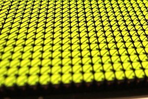
The display tube has 100 anodes (in the default mounting orientation going horizontally from left to right) and a 100 cathodes (going vertically from top to bottom). Whenever the voltage between an anode-cathode pair goes above 235V the pixel on their intersection begins to glow and is extinguished when the voltage goes below 100V (according to the lamp's datasheet).
See https://en.wikipedia.org/wiki/Neon_lamp for how the lamp works in more detail.
The anodes are pulled up constantly to 240V via 390kΩ resistors, and selectively pulled down via 330kΩ using the КН1150КН1 nMOS array (very similar to Sony LZ1032A). Each nMOS array has a TTL compatible shift register built in, which is filled with the data of the whole vertical line to be displayed. There are 2 groups on Anodes, so the loading of data is not as simple as clocking all bits in sequence, but I'll get to that later.
When it comes to the cathodes, only 80 out of the 100 are connected to the driving circuit. They're arranged in a groups of 5 driven, 1 not connected and additionally some not connected on the edges. Because the display was originally intended to only show 5x7 pixel characters the vertical lines between the letters weren't needed.
Maybe in the next version of the project I'll add driving circuits to the missing cathodes. It would be great if the wires are soldered to the PCB but if they're not I'm not going to risk breaking the neon tube when separating the epoxy glued PCB.
The cathode selection circuitry is much simpler there's an array of high volatage NPN transistors (packed 4 per IC) where the collector is connected to the cathode, the base and emitter are driven by TTL logic pull-downs and 1kΩ pull-ups to 5V on the Anode Driver PCB. Whenever the Base is pulled up to 5V and the Emitter is pulled down to 0V the cathode connected to the Collector is active.
The arrangement of the TTL decoders and not gates guarantees that there's at most 1 Base pulled up and at most 1 Emitter pulled down at the same time.
The MS-6205 came out in different versions (looking at schematics it was probably dependent on IC availability), but the external electrical interface was kept the same and the neon matrix lamps used were very similar.
The model that I have consists of (going in order from the neon matrix):
For people who don't have connector labels: if you orient the display so that the side with the connector is facing you and the neon matrix is facing down (see zoomed in connector corner photo). Then row A is the bottom one, row B (Б) is the top one. The pins are numbered starting with 1 on the right and ending with 32 on the left. If your connector has a group of 3 pins, then a gap, you should count the gaps too so that it all adds up to 32. Be aware that in your version of the display the connector can be rotated 180°, row A is always the one with the widening notches.
To complete my project It should be enough to replace the Logic PCB (maybe except for the high voltage generator) and start controlling the pixels while skipping the character page/character ROM logic completely.
Create an account to leave a comment. Already have an account? Log In.
Become a member to follow this project and never miss any updates

 Arduino Enigma
 Jacob Still
 Stephen G
 Frederic L