Close
0%
0%

Sinclair Scientific Calculator Emulator

A register level TMS0805 CPU emulator on an Arduino Nano runs the original 320 instruction calculator program. A custom PCB houses it all.

Similar projects worth following
Understanding the architecture of past, simpler CPUs is important to learn how to create future devices.

This project implements an accurate emulation of the Sinclair Scientific Calculator. Most of the display glitches are accurately duplicated. The components in this project are easily sourceable, thus it should be able to be replicated.

The original chip inside the Sinclair Scientific Calculator was reverse engineered by Ken Shirriff, its 320 instruction program extracted and an online emulator written. This project ports that emulator, written in Javascript, to the Arduino Nano and interfaces it to a custom PCB. The result is an object that behaves like the original calculator, with its idiosyncrasies and problems. Calculating PI as arctan(1)*4 yields a value of 3.1440.

Special care was taken in the design of the emulator to match the execution speed of the
original calculator, which varies from acceptable to atrocious for trigonometric functions involving small angles.

This project documents how to turn a web page into a functioning physical object. It has a hardware and a software side. 

The software side of this project is a port to the Arduino platform of the original Sinclair Scientific Calculator simulator (http://righto.com/sinclair). 

The hardware part has evolved over time. It started as a quick modification to the Kim UNO by @Oscarv  (http://obsolescence.wixsite.com/obsolescence/kim-uno-summary-c1uuh) with the keys arranged in the Sinclair pattern and a 9 digit display.

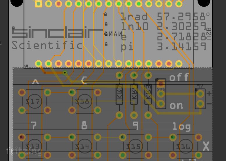
Over time, the PCB has evolved, over two iterations the width has been reduced to match that of the original calculator. The keyboard on the latest version is dimensionally accurate. Its keys line up with the buttons on the real calculator. 

By experimenting with a real Sinclair Scientific calculator, the connections between the keyboard and the display digits were deduced. An accurate schematic has been created, its correctness verified by pressing simultaneously multiple keys on the calculator and observing that the display glitches in the same way in the original and the emulator. 

This has turned the V5 and V6 PCBs into the most accurate emulators out there.

The V5 PCB is limited in height to 100mm so it can be manufactured inexpensively. 

The V6 PCB has the same accurate keyboard and display circuit as V5 and is also dimensionally accurate at 110 x 51mm.

A version using bubble LED displays is in the works depending on the continued availability of those modules.


Open Source Licenses:

The original TI / Sinclair simulator is licensed under GPL v2 so the Arduino port is also licensed under GPL v2

The PCB files are:

Creative Commons License
Sinclair Scientific Calculator Emulator by @ArduinoEnigma is licensed under a Creative Commons Attribution-ShareAlike 4.0 International License.
Based on a work at http://righto.com/sinclair.


Project Logs in chronological order:

11/17/2017 - The keyboard is designed.
https://hackaday.io/project/91895-sinclair-scientific-calculator-emulator/log/121215-11172017-the-keyboard-is-designed

12/21/2017 - A suitable display is found, design of the PCB continues.
https://hackaday.io/project/91895-sinclair-scientific-calculator-emulator/log/121370-12212017-a-suitable-display-is-found-design-of-the-pcb-continues

12/23/2017 - Putting the Display and Keyboard together.
https://hackaday.io/project/91895-sinclair-scientific-calculator-emulator/log/122095-12232017-putting-the-display-and-keyboard-together

12/25/2017 - Finished Routing the Board and Submited for Production (how to do tented vias in Fritzing)
https://hackaday.io/project/91895-sinclair-scientific-calculator-emulator/log/123664-12252017-finished-routing-the-board-and-submited-for-production

12/30/2017 - The desire to design a slimmer version begins
https://hackaday.io/project/91895-sinclair-scientific-calculator-emulator/log/125443-12302017-the-desire-to-design-a-slimmer-version-begins

01/03/2018 - The manufactured V1 boards arrive
https://hackaday.io/project/91895-sinclair-scientific-calculator-emulator/log/125513-01032018-the-manufactured-v1-boards-arrive

01/05/2018 - V1 is assembled, a problem appears
https://hackaday.io/project/91895-sinclair-scientific-calculator-emulator/log/125515-01052018-v1-is-assembled-a-problem-appears

01/06/2018 - Work on the Arduino port of the TMS0805 Simulator continues
https://hackaday.io/project/91895-sinclair-scientific-calculator-emulator/log/126356-01062018-work-on-the-arduino-port-of-the-tms0805-simulator-continues

01/07/2018 - Using a fast pin library to improve performance
https://hackaday.io/project/91895-sinclair-scientific-calculator-emulator/log/126425-01072018-using-a-fast-pin-library-to-improve-performance...

Read more »

V5 Schematic.png

V5 Schematic. Download gerbers at https://oshpark.com/shared_projects/OSfM0RLN

Portable Network Graphics (PNG) - 89.68 kB - 03/30/2018 at 01:59

Preview

roundedrect50x100.svg

This is a custom PCB shape. A 50x100mm rectangle with 3mm radius corners.

svg+xml - 2.40 kB - 04/18/2018 at 21:10

Preview

SinclairScientificCalculatorV1-RC2-Hackaday.zip

Fritzing File for the Sinclair Scientific Calculator Emulator PCB

x-zip-compressed - 56.48 kB - 03/25/2018 at 01:54

Download

View all 10 components

  • Happy Pi Day 2019 Sinclair Scientific Style

    Arduino Enigma03/15/2019 at 06:02 0 comments

  • New version using Bubble LED Displays

    Arduino Enigma07/04/2018 at 18:03 1 comment

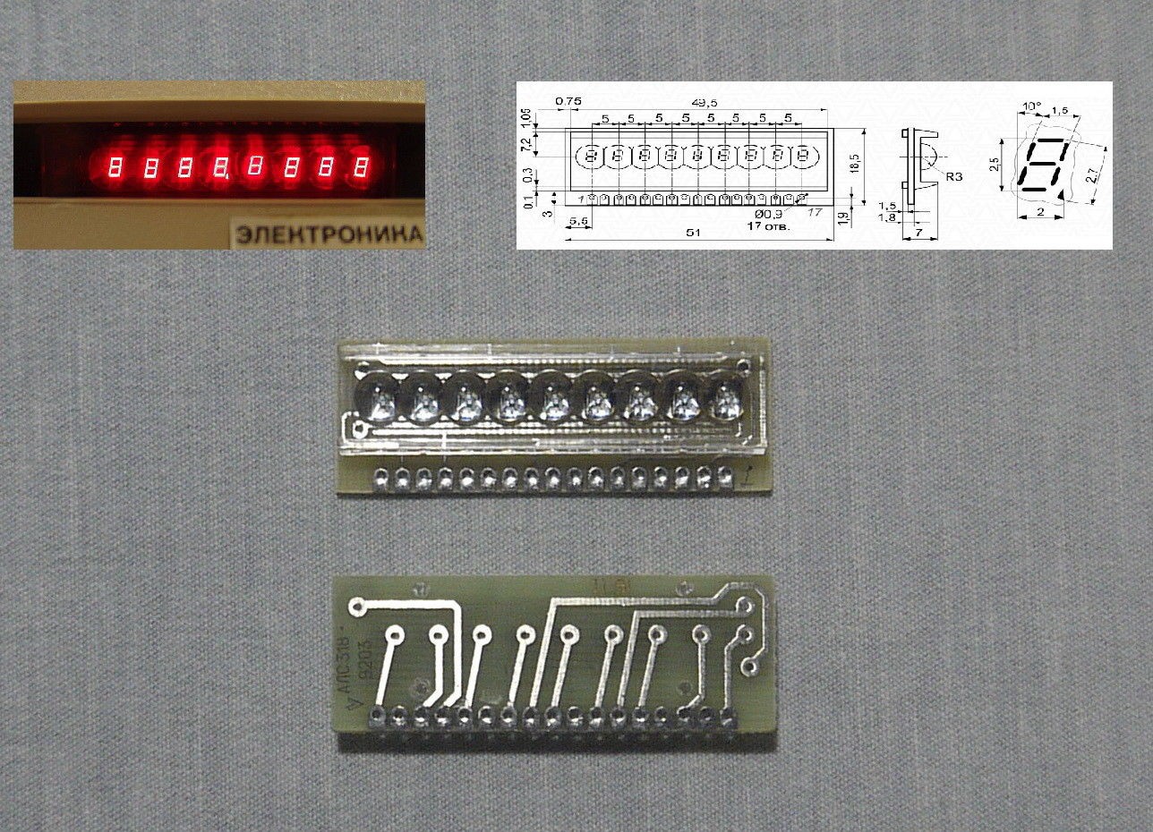
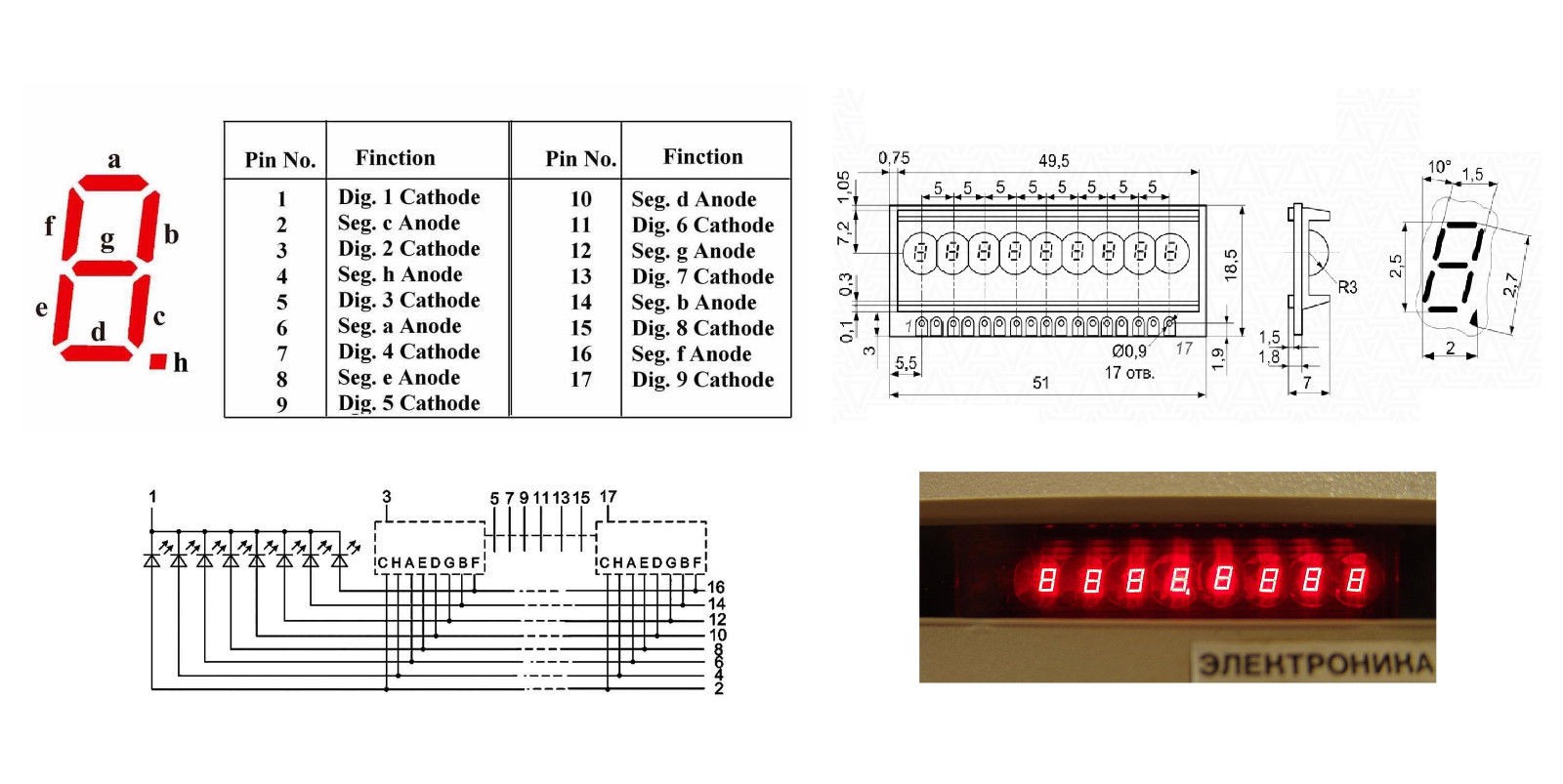
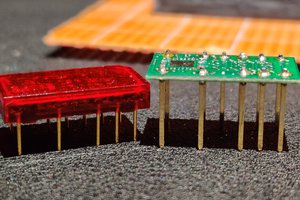
    Browsing through ebay, looking for a bubble led display to give the calculator a more authentic look, the following product appears. It is supposed to be a Russian made clone of the HP 5082-7441 9 digit bubble display. With a horizontal dimension of 51mm, it will fit inside the Sinclair Calculator PCB.

    The following datasheet is provided. The display is common cathode. The pin spacing is metric. The connector has 17 pins and it alternates between a digit selection cathode and a segment anode. It does not look too hard to connect to the existing calculator circuit.

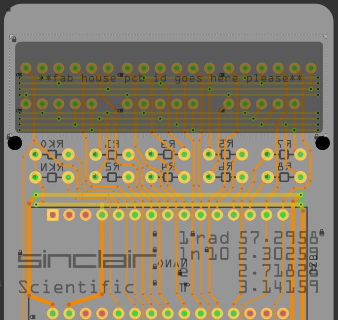
    To replace the modern LED modules in the calculator with a bubble display, first the LED modules will be deleted, and the current limiting resistors will have to be moved down to accommodate the increased height of the bubble module. The change from a common anode to a common cathode display will be handled exclusively in software. The only wiring change is that RK0 and RKN will be changed from pulldown to pullup resistors.

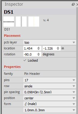
    Sometimes, just sometimes, Fritzing comes through by having the exact component one is looking for. In this case, a parametric connector. The amount of pins (17) and the pin spacing (2.5mm) can be specified. Looks like this will be an exact fit.

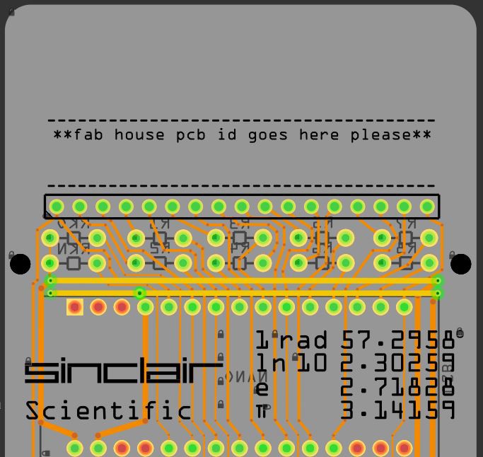
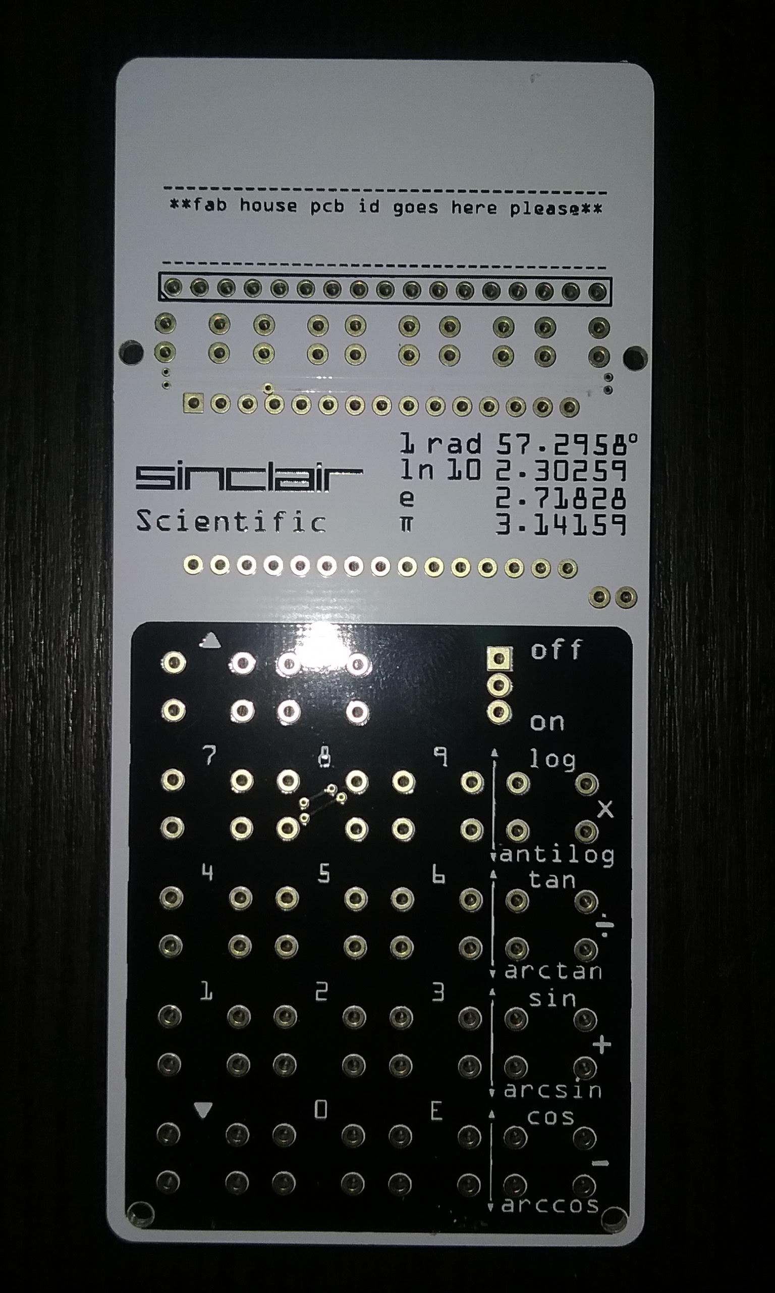
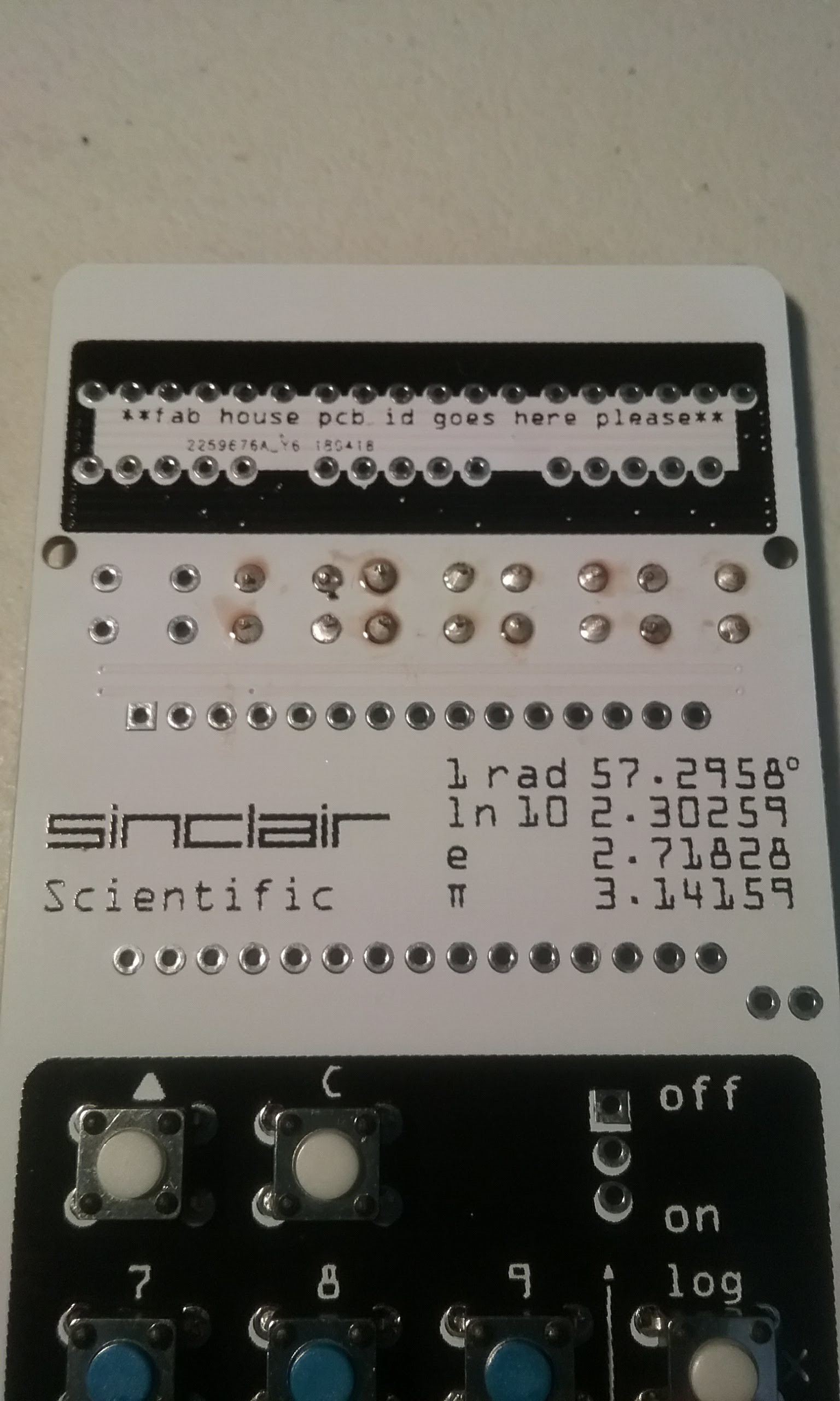
    The new PCB is laid out with the new connector and a space is dedicated for the fab house to put their job number. We do not want those extra markings in an inconvenient place, like next to the Sinclair logo. It has happened before. As an interesting note, there is no copper above the 17 pin connector. Note that RKO and RKN are now pull up resistors.

    We will be ordering this board from PCBWay.com The ordering process is the usual, describe the size, layers, thickness, board color and decide if the boards will be Lead-free or ENIG finish and submit the Gerbers.

    When placing an order, try selecting a few more boards than you want and see what it does to the price quoted. In this case, I was able to get 20 boards instead of 10 for a few bucks more.

    While ordering, you can also take advantage of the Free Universal Boards option and get some free perfboard for some future projects.

    While the boards are being fabricated, the progress can be tracked.

    48 hours later, the package is handed to DHL and 3 days later it shows up. One gets spoiled after trying DHL express, order boards and receive them in 5 days including weekends. 

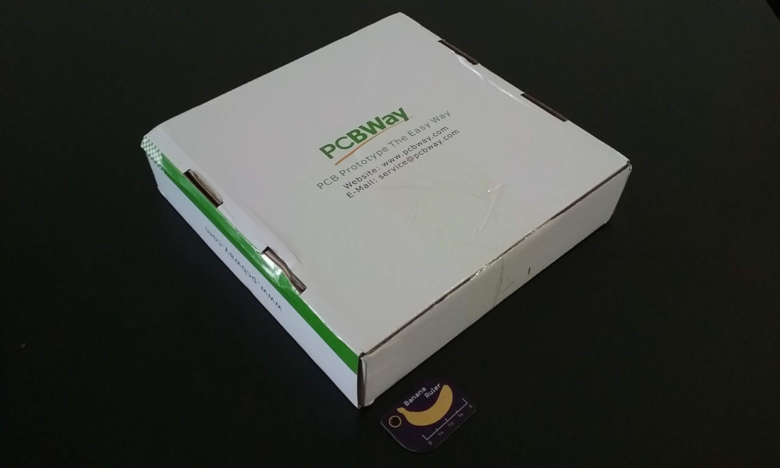
    Inside is this good looking box. Banana for Scale.

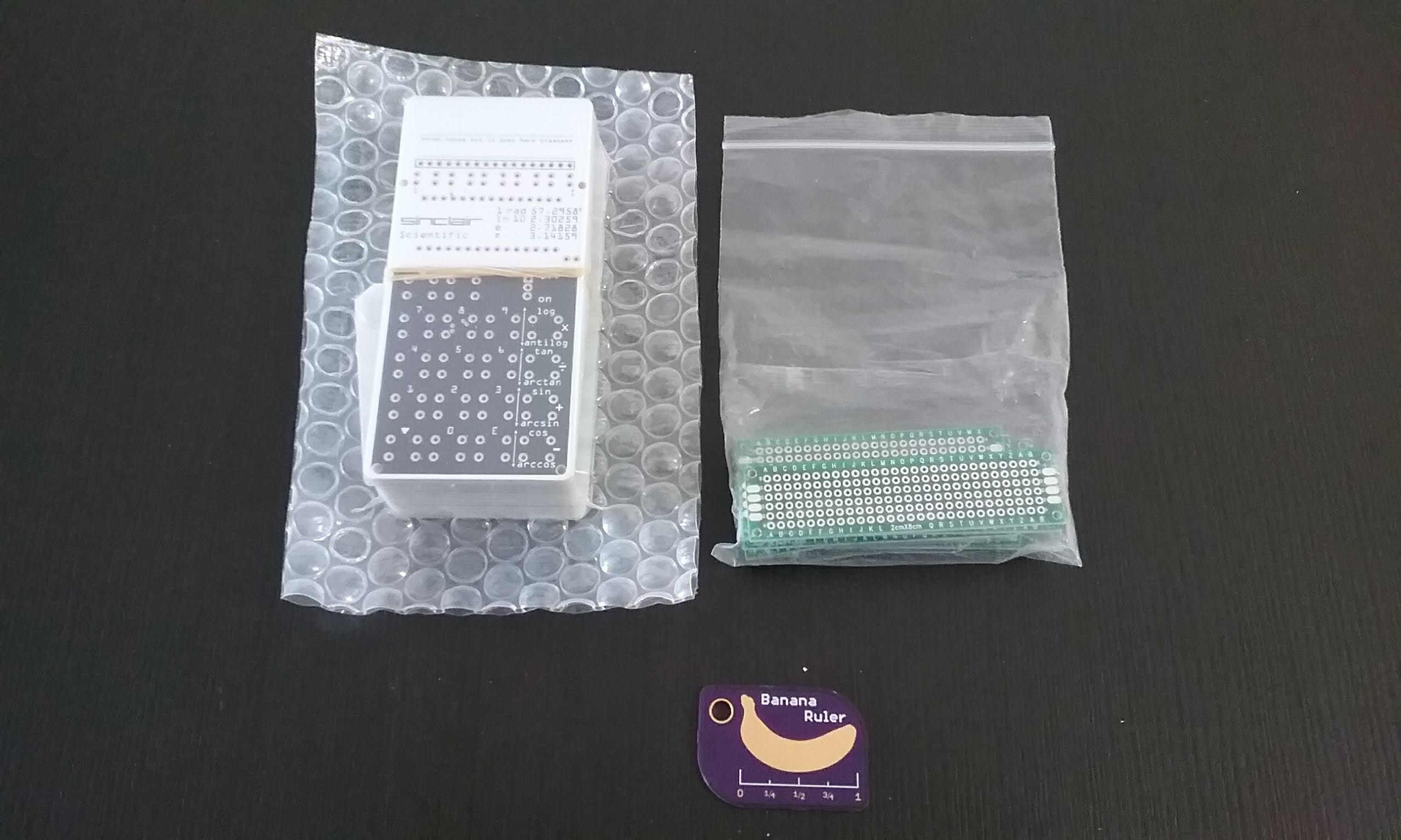
    The boards are packaged in the usual combination shrink/bubble wrap. The free perfboards are nice...

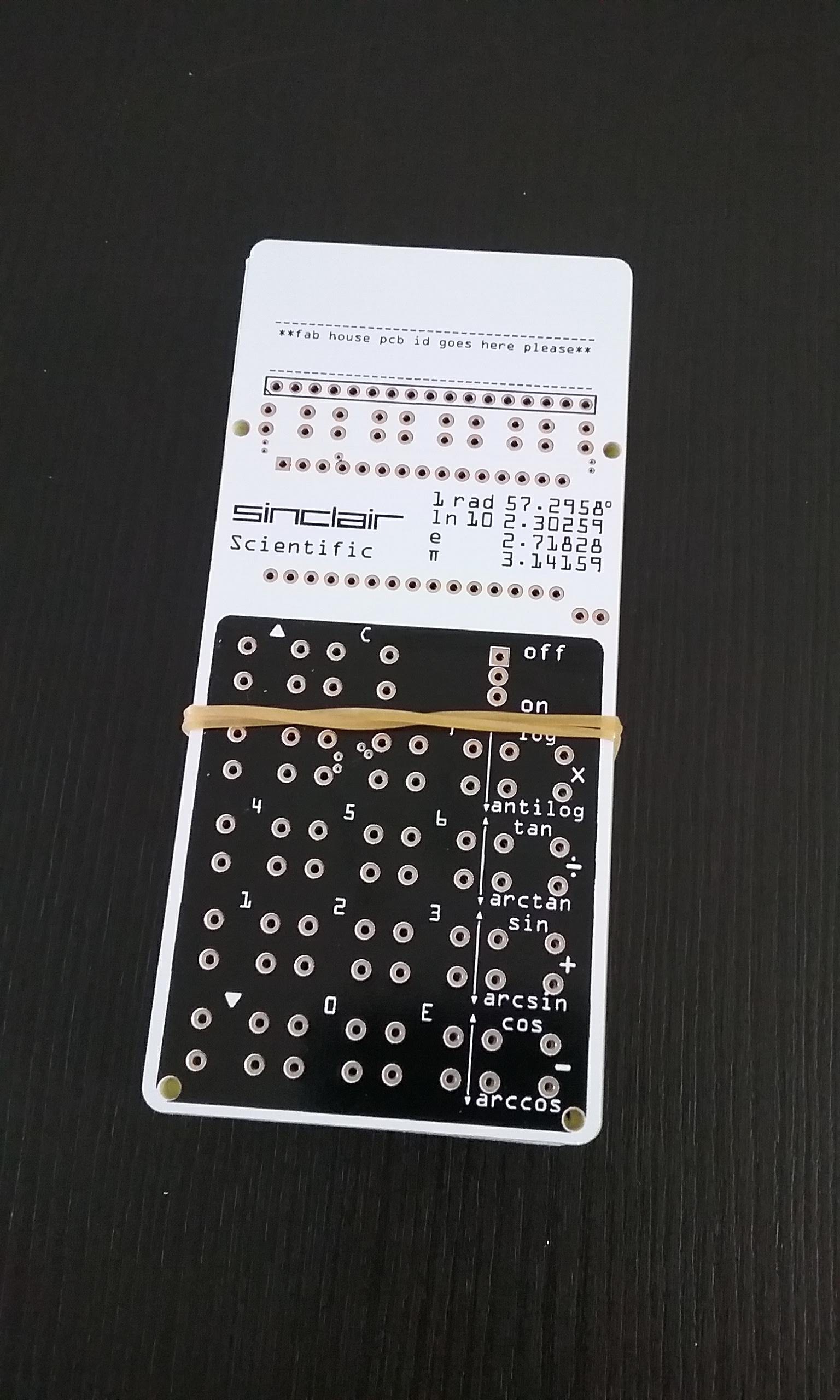
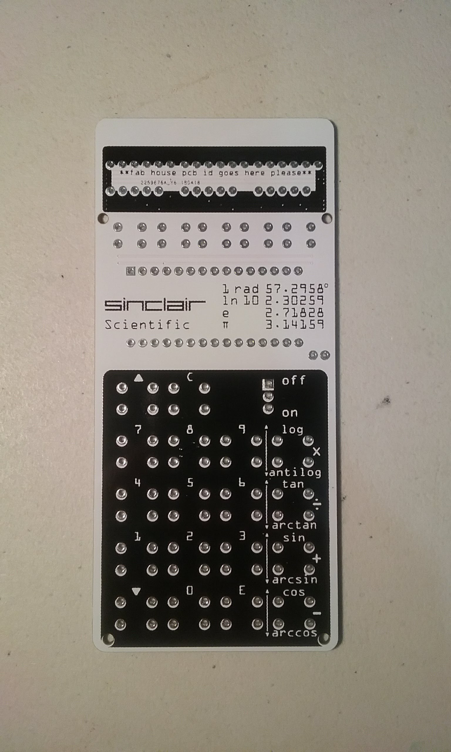
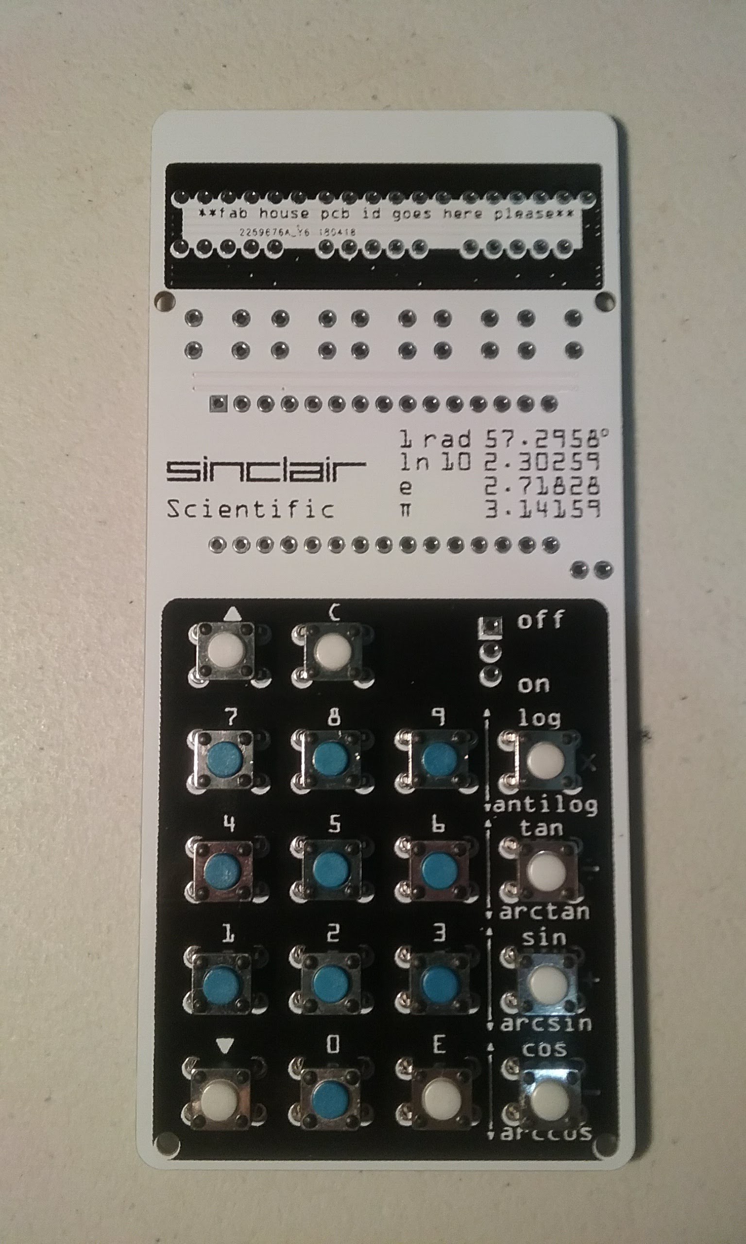
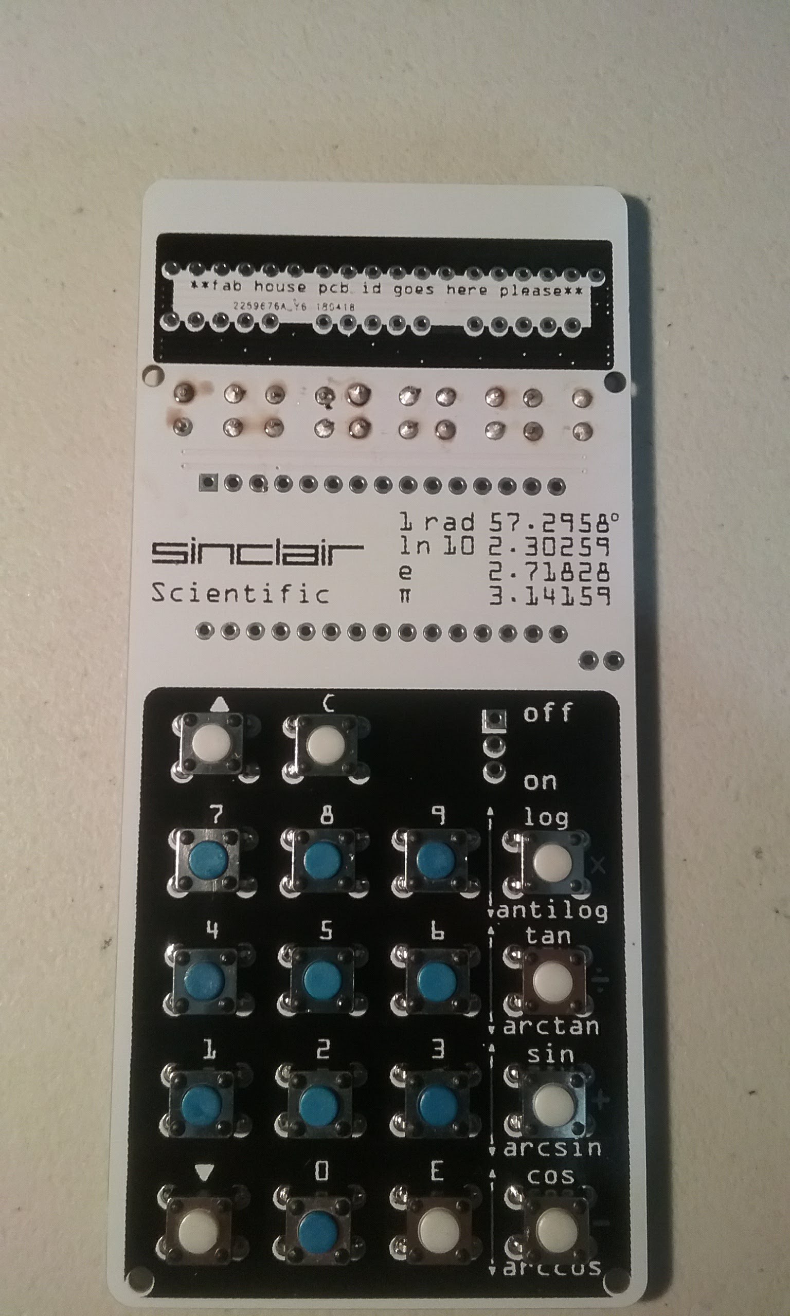
    I have opened PCB orders and been thoroughly disappointed before. Everybody can get the Sinclair logo and the text right but the large negative silkscreen in the keyboard is difficult to do correctly. Not this job. The board is perfect. The white soldermask covers the tracks nicely and the black silkscreen is sharp.

    The board was plated with Electroless Nickel Immersion Gold (ENIG) .

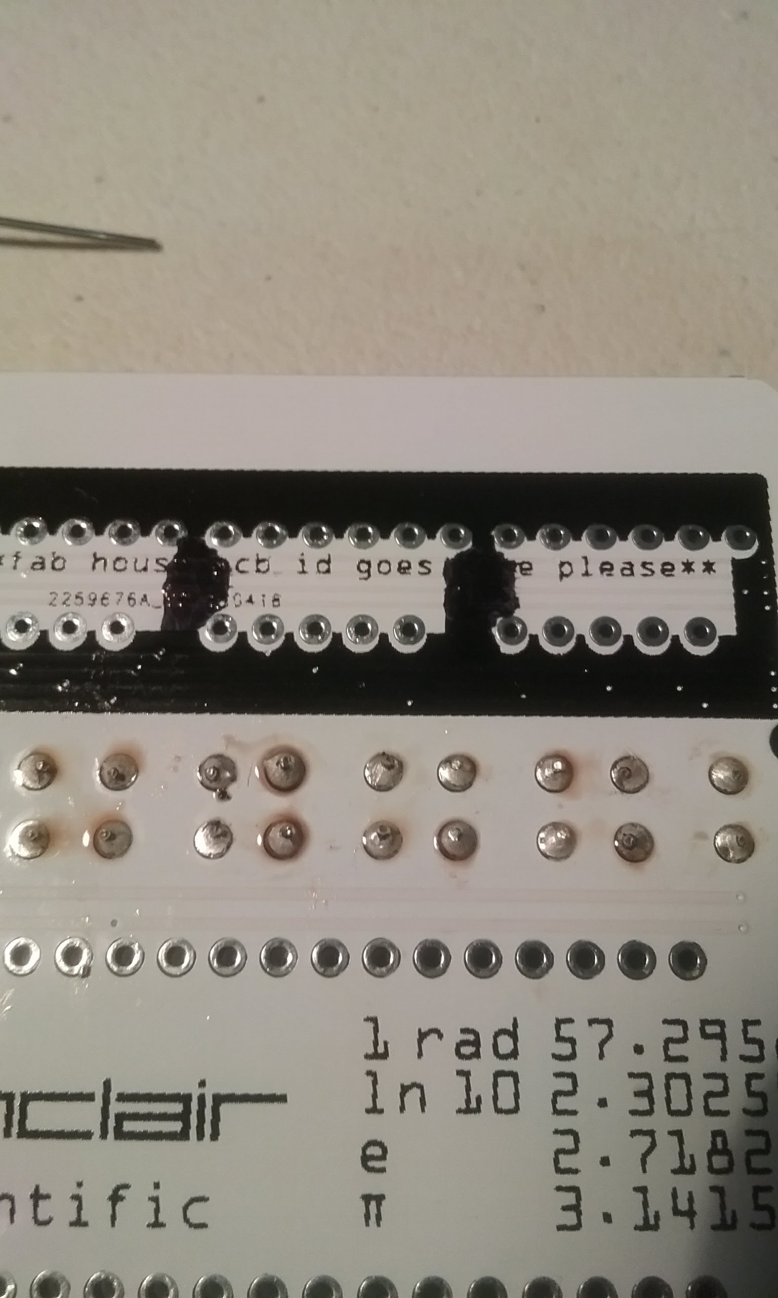
    There is no job number in the area that was dedicated to this marking. It's nowhere to be found. Maybe they do not need to mark the boards, I think to myself. 

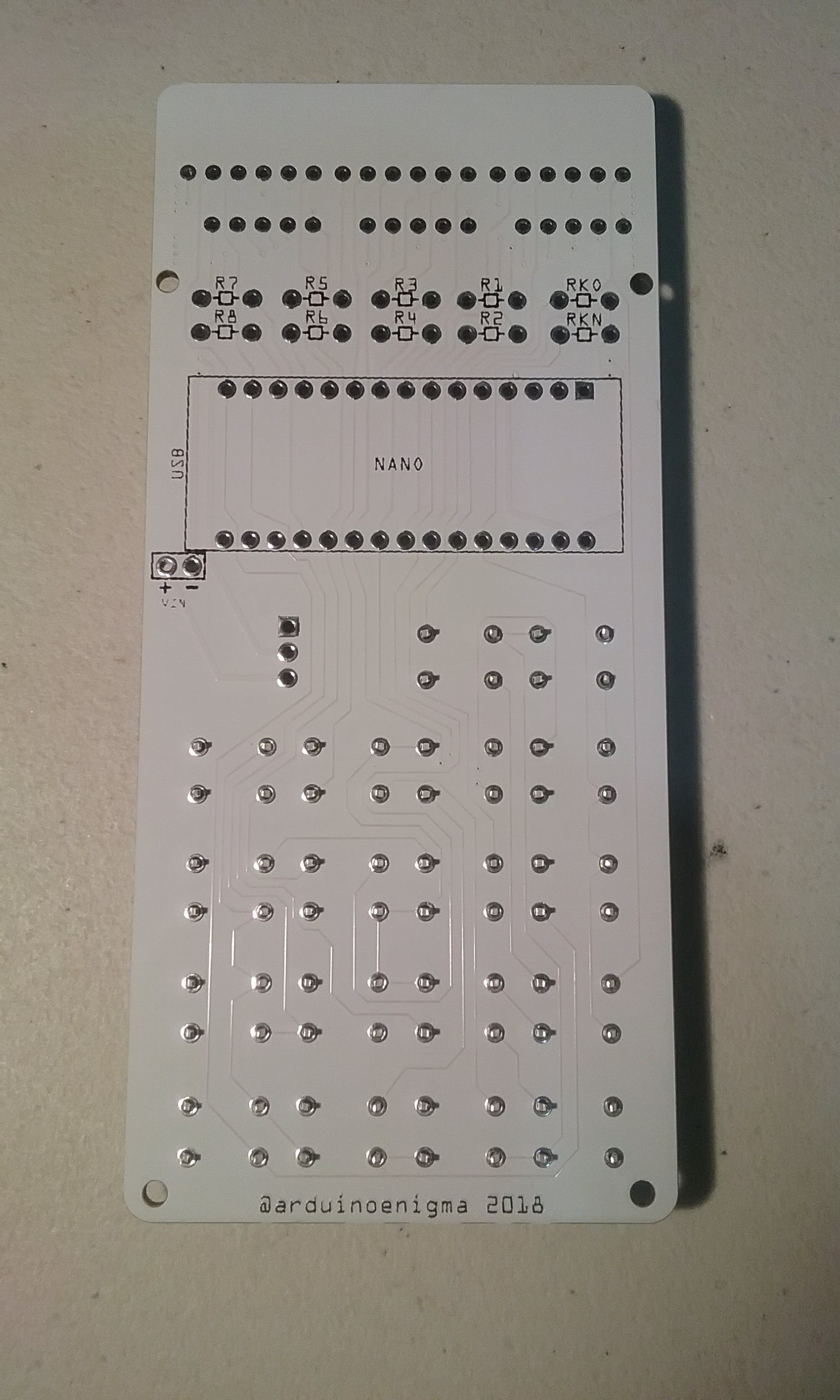
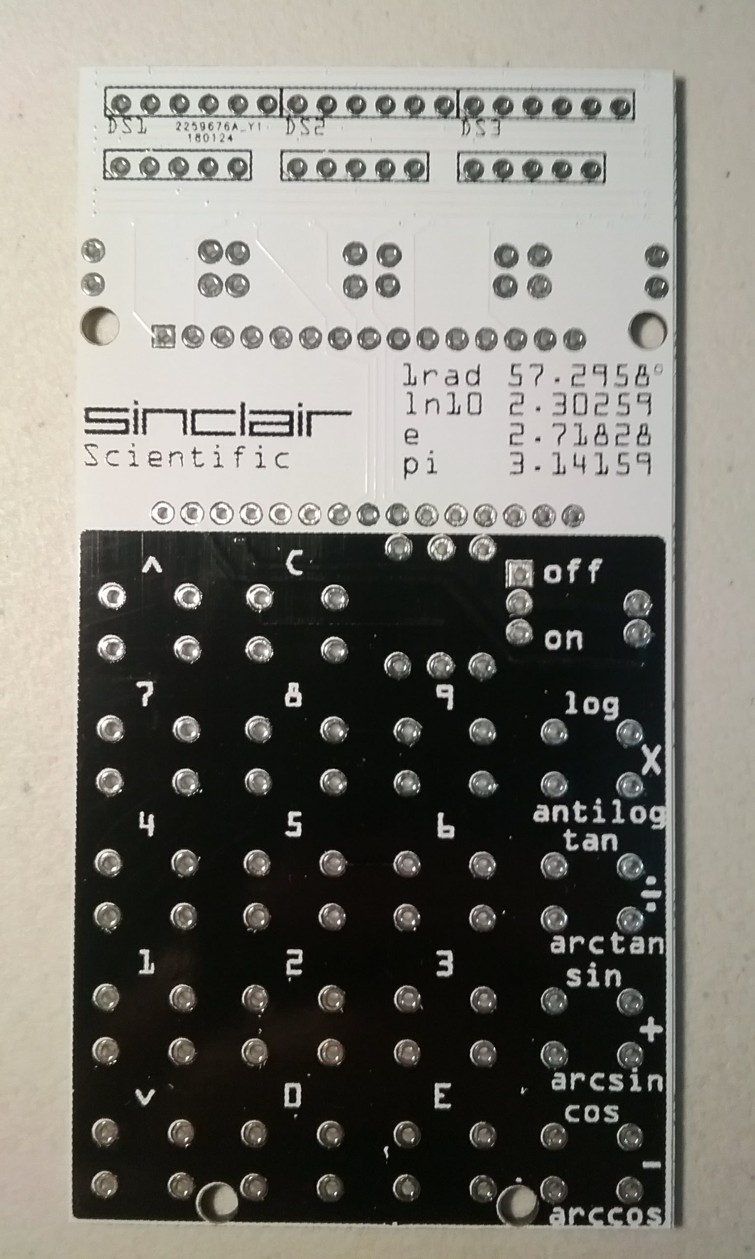
    The back of the board also looks good. Then I see it. The job number was placed inside the footprint for the Arduino Nano. Not a bad choice as it will be hidden once the Nano is soldered.

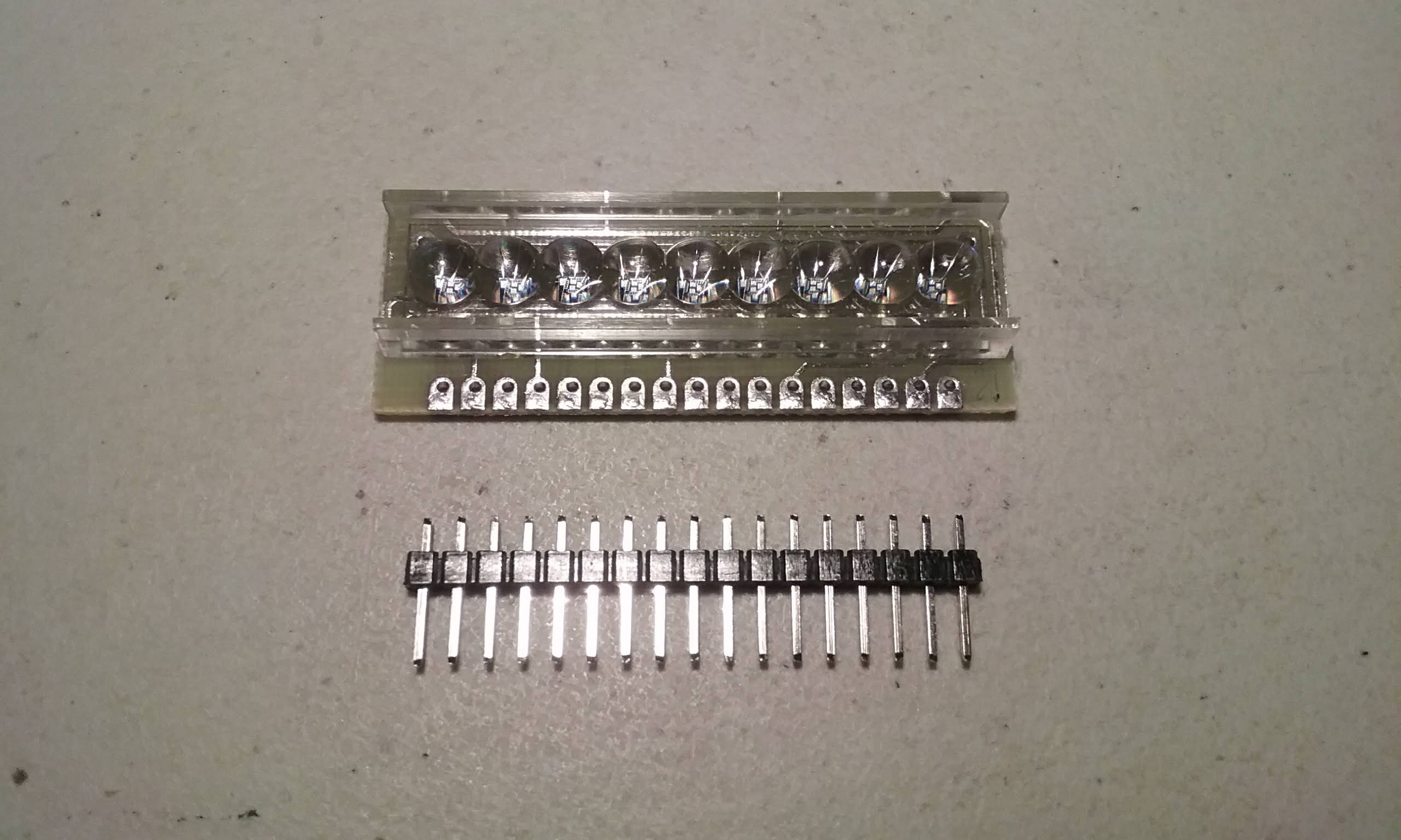
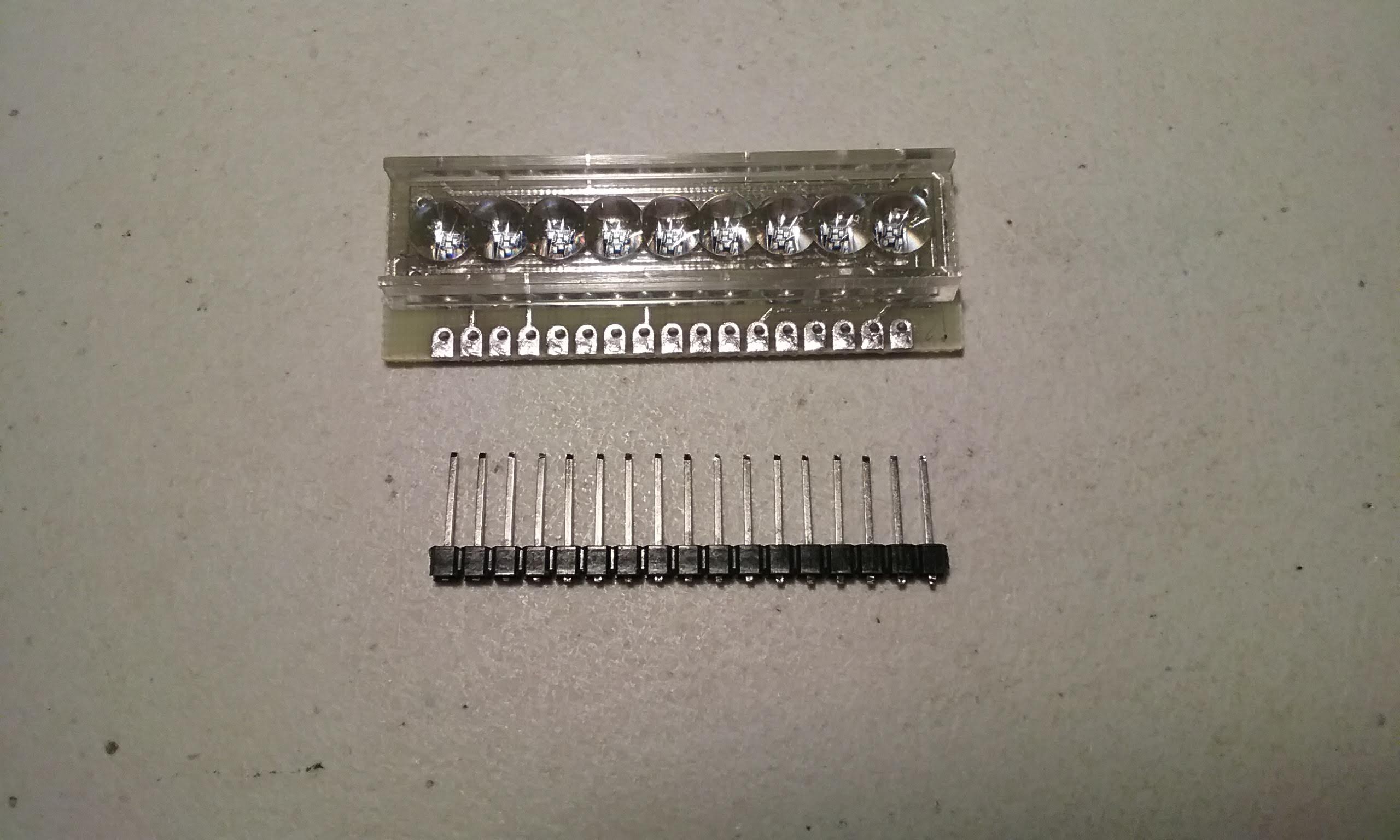
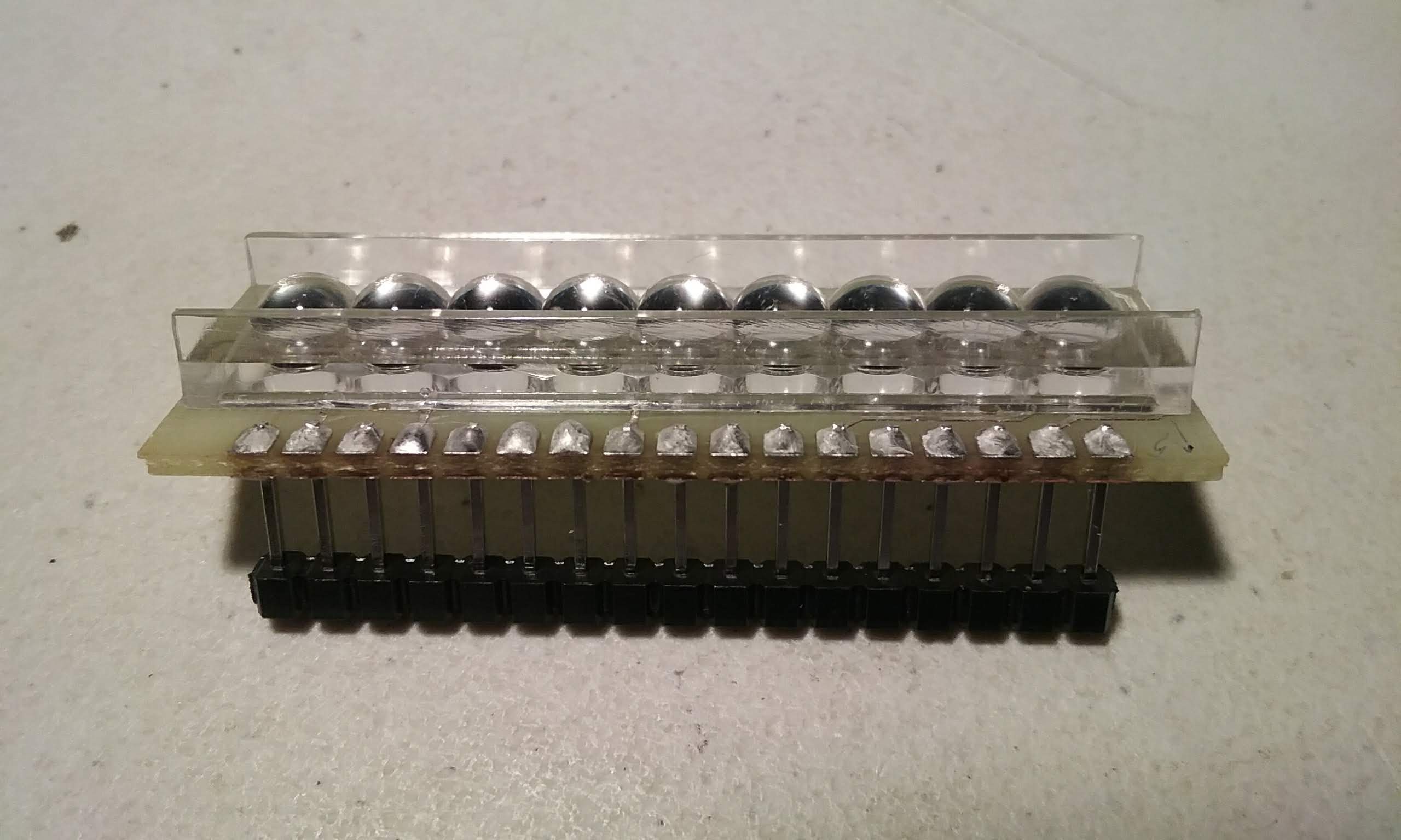
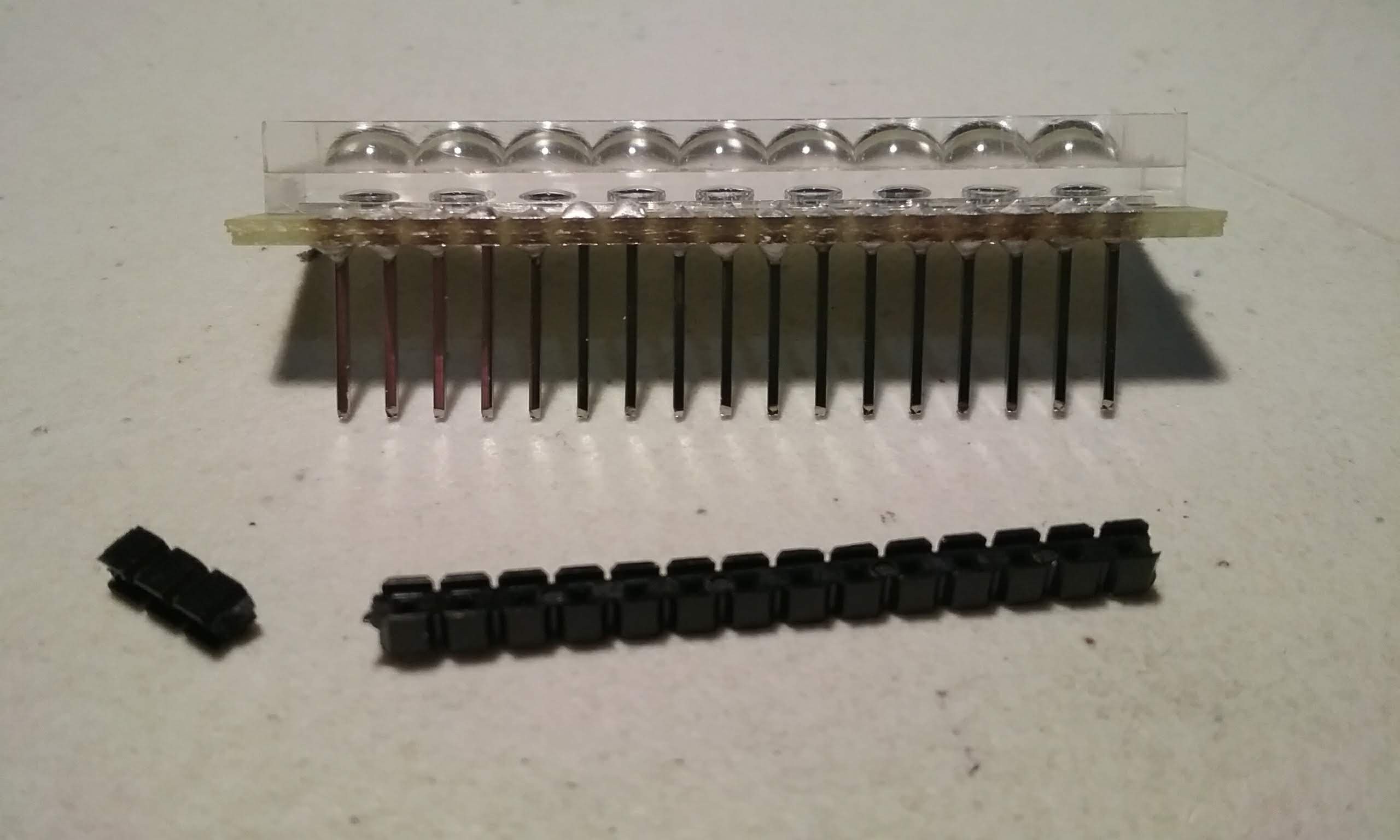
    The display comes without headers. I only have  0.1 inch (2.54mm) pitch pins. The display is 2.5mm pitch. 

    To make it fit, first the spacer is slid down towards the end of the pins.

    That allows the other end of the pins to fit into the display. Arrange the pins so they barely protrude from the pads.

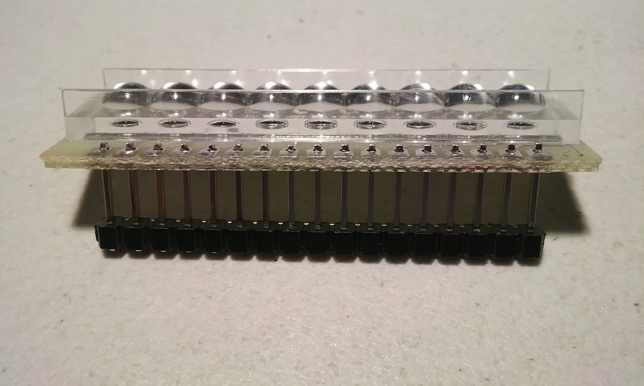
    Finally, solder all the pins.

    Once that is done, the spacer can be removed. 

    And the display can be test-fitted. Looks...

    Read more »

  • Assembly Instructions for PCB v6

    Arduino Enigma04/26/2018 at 22:24 0 comments

    This log will show how to assemble your own Sinclair Scientific Calculator emulator. 

    First we start with the blank PCB.

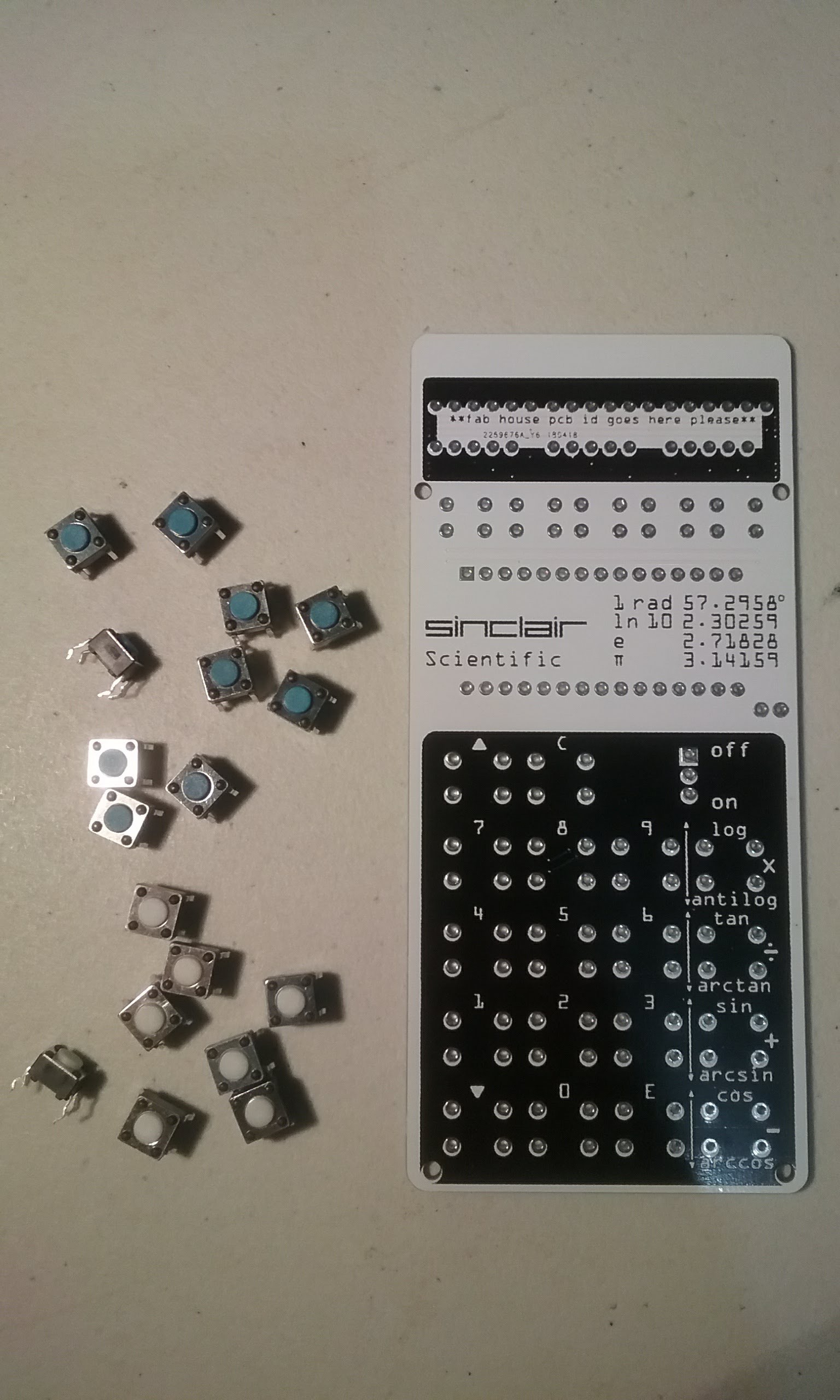
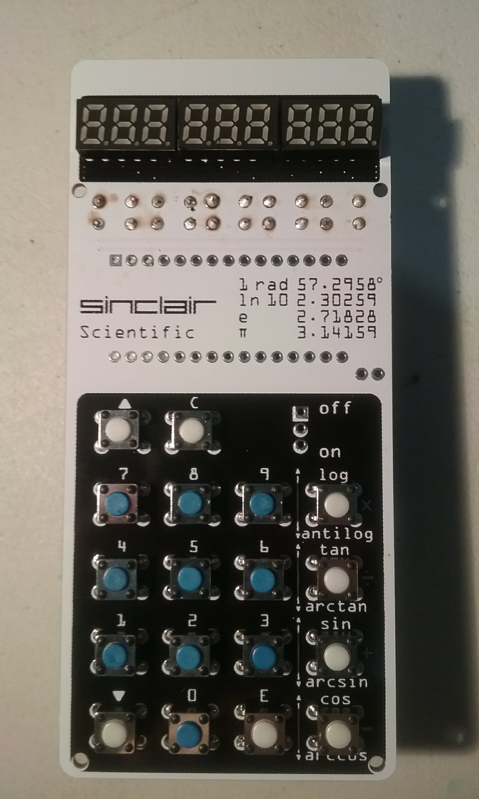
    Separate the buttons. You should have 10 blue buttons and 8 white buttons.


                      ---- WARNING!!! ---

    If you have purchased a kit, the calculator comes with the buttons and displays installed just to prevent damage during shipping. The blue buttons need to be removed and installed in their correct positions, the number keys.

    The blue buttons go in the number keys, the white ones go in the function keys. See WARNING above. 

    The buttons pins are wider apart on the horizontal dimension, so they only go in one way. Make sure no pins are bent on the way in. 

    The buttons act as jumpers to the bottom copper layer so all the legs must go in and be soldered. Normally, the top two pins are internally jumped, and the bottom two pins are also jumped. When the button is pressed, continuity is established between the top and bottom pins. 

    Flip the PCB over and make sure all the pins are in.

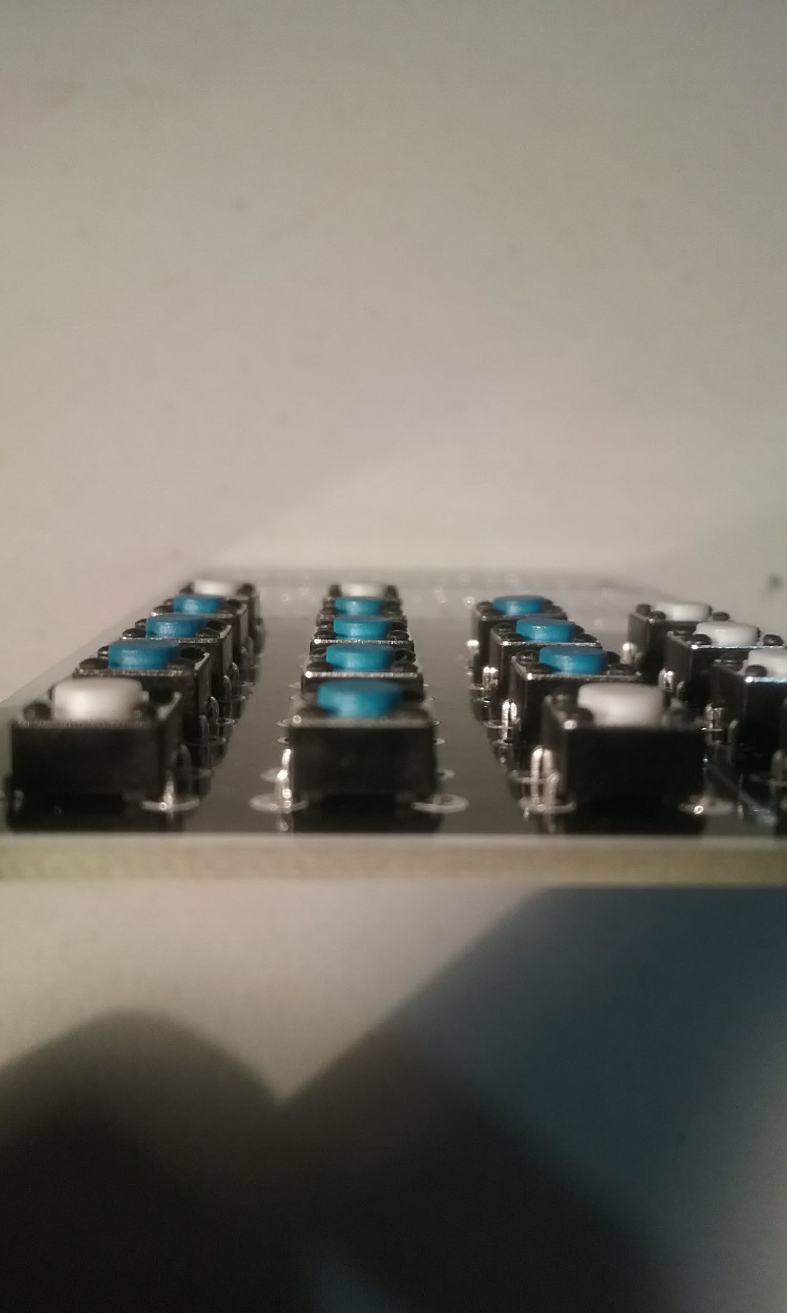
    Flip the PCB again and make sure all the buttons are aligned. Once they are soldered they are kind of hard to straighten out. I check them often during soldering to make sure none has popped out..

    Solder all the buttons. I like to go top to bottom starting on the far right column. Examine the solder joints and rework if necessary.

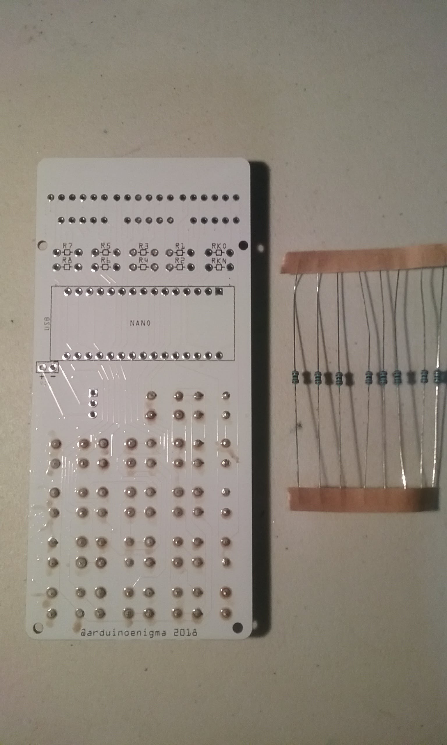
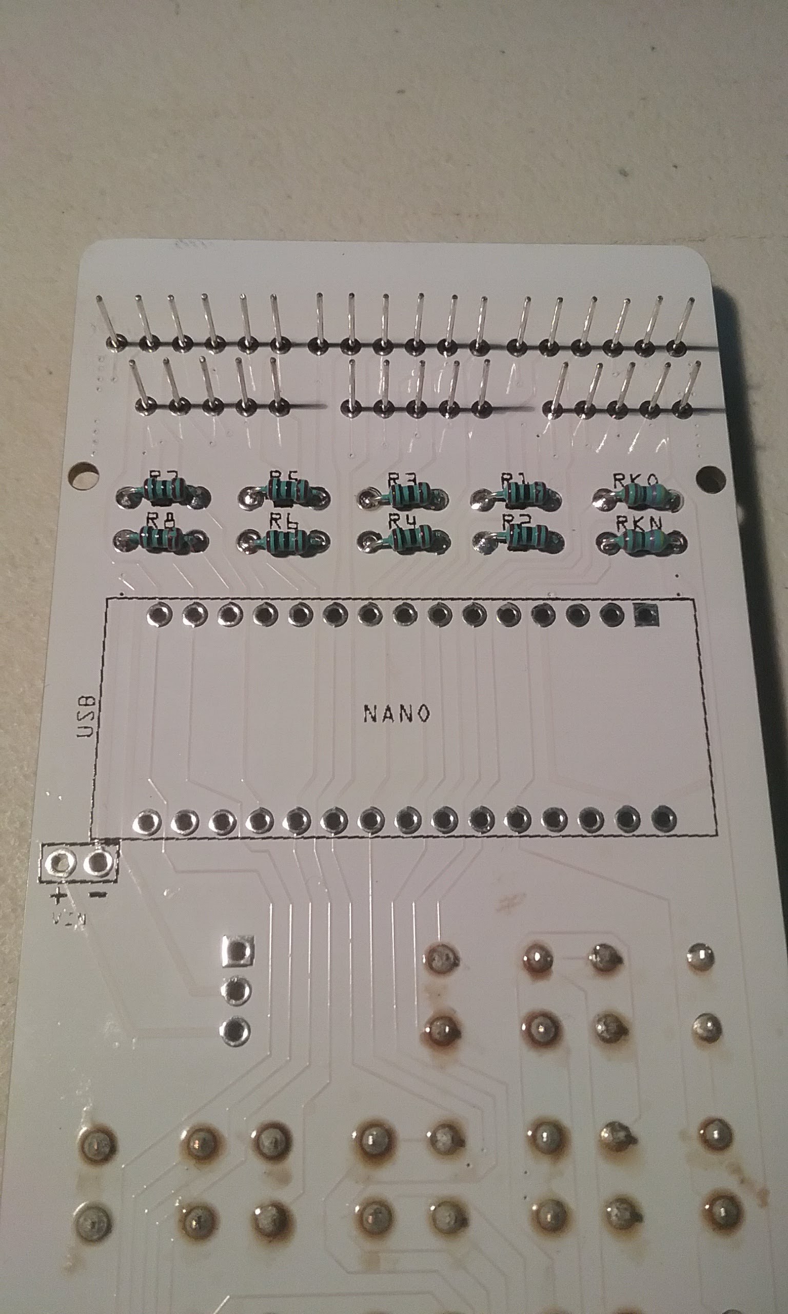
    After the buttons are soldered, next is the current limiting resistors turn. These set the intensity of the LEDs. Smaller values will make the LEDs brighter, but shorten the battery life.

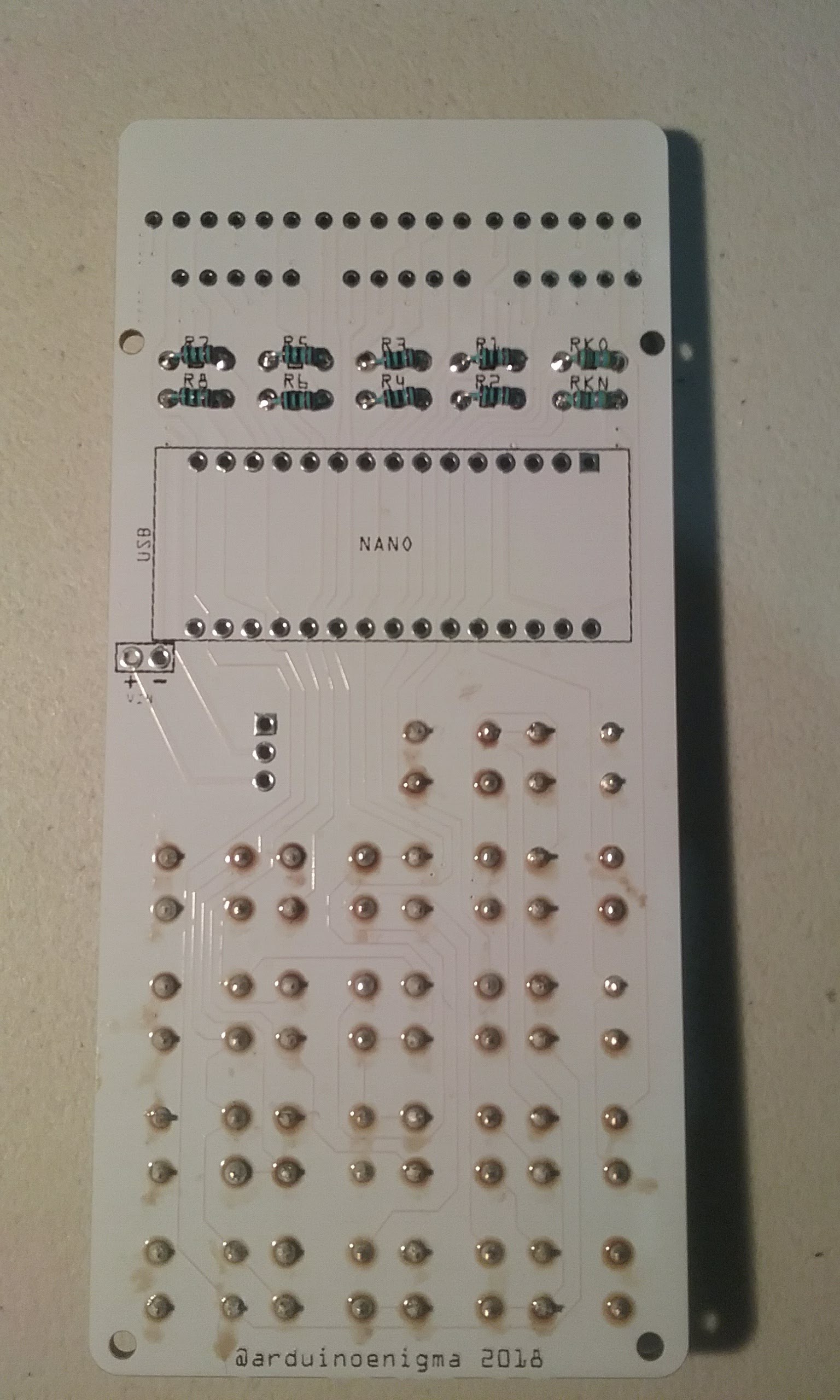
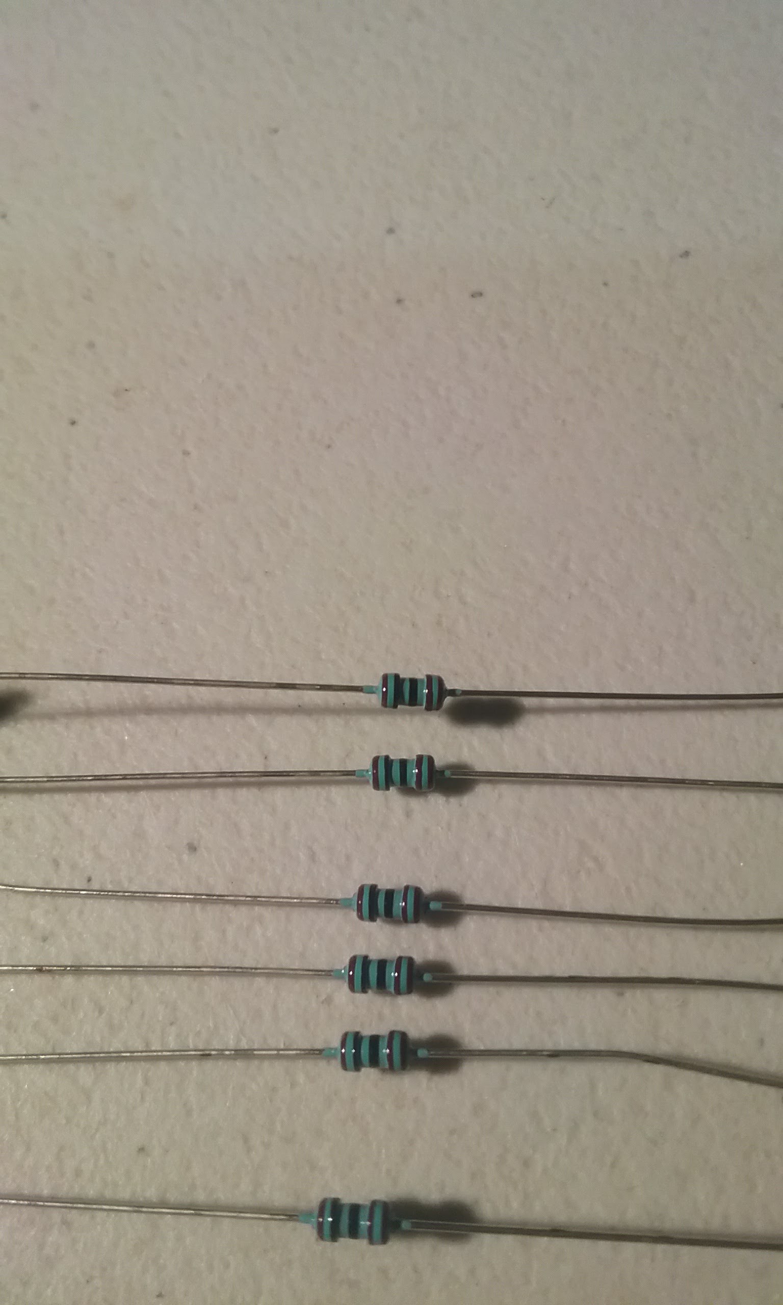
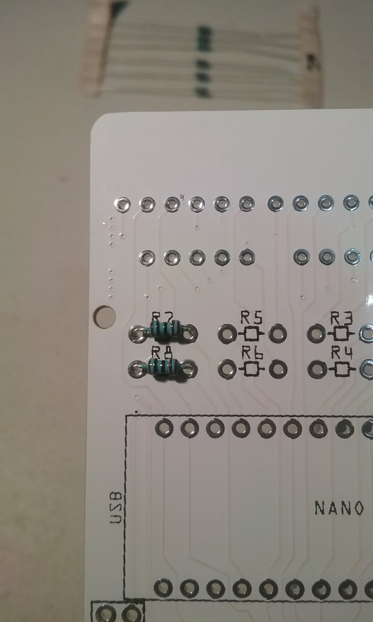
     Find the strip with 8x 1K resistors. Those will go on R1 through R8. Do not populate RKO and RKN at this time. Do not confuse the resistors or the brightness of individual segments will be different.

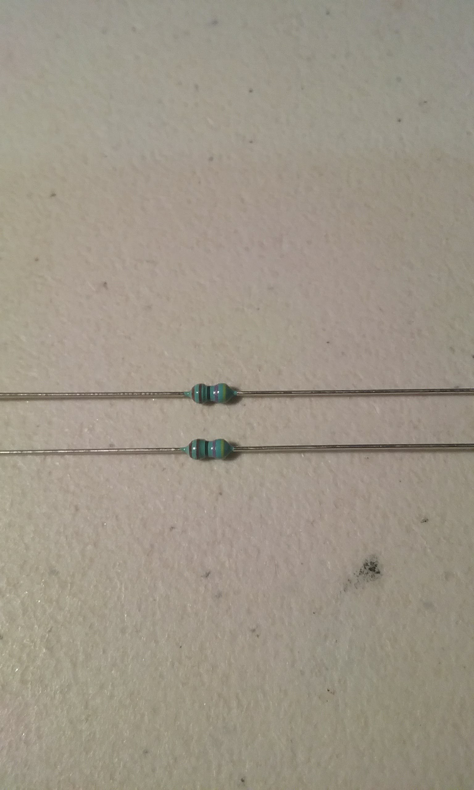
    A close up of what a 1K is supposed to look like, brown and black lines. The 4.7K have a yellow band on one end.

    Bend the legs close to the body and insert from the bottom of the board. 

    Flip the board and while pushing down, solder the legs. 

    Once soldered, trim the legs.

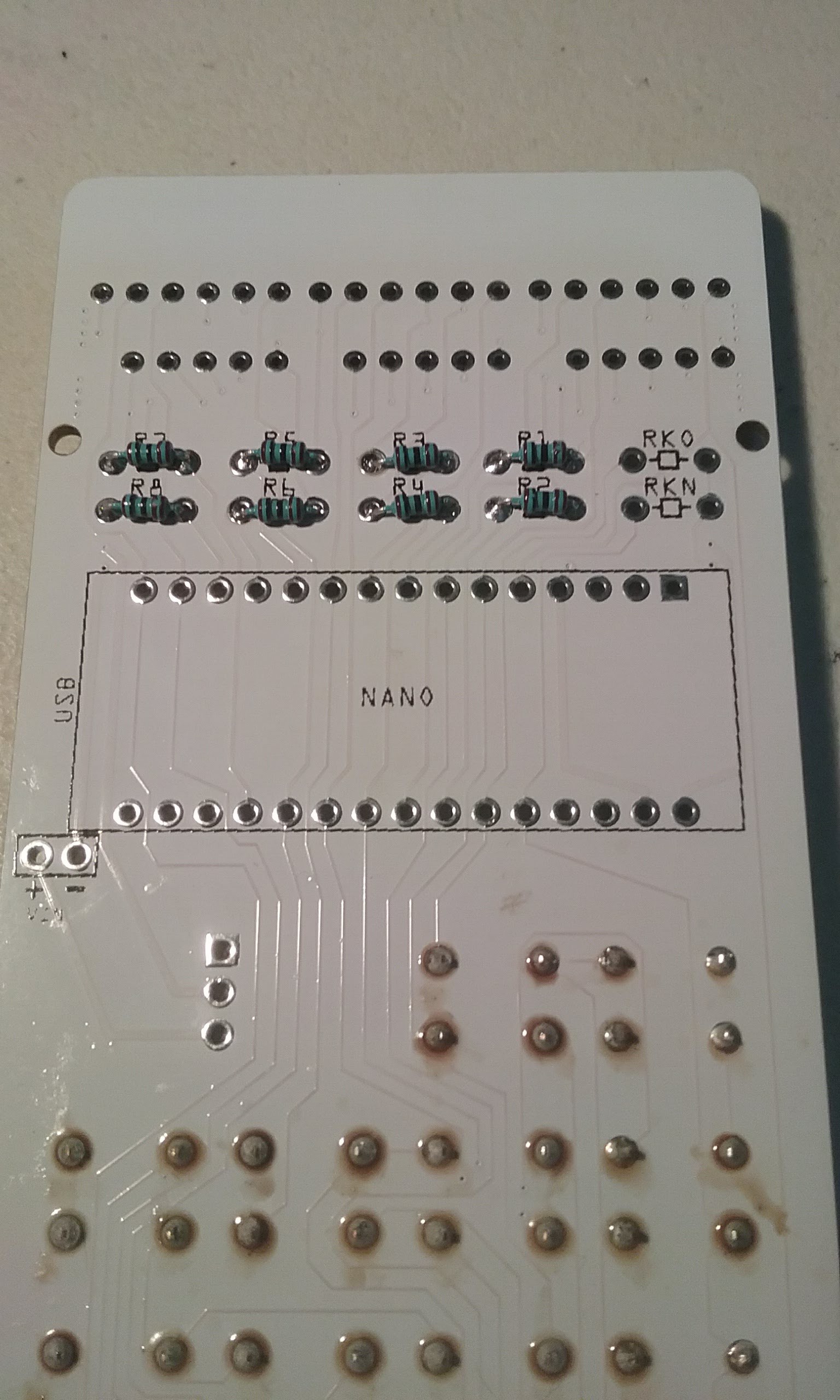
    Continue doing two at a time until R1 through R8 are populated.

    This is how the board is supposed to look like at this point.

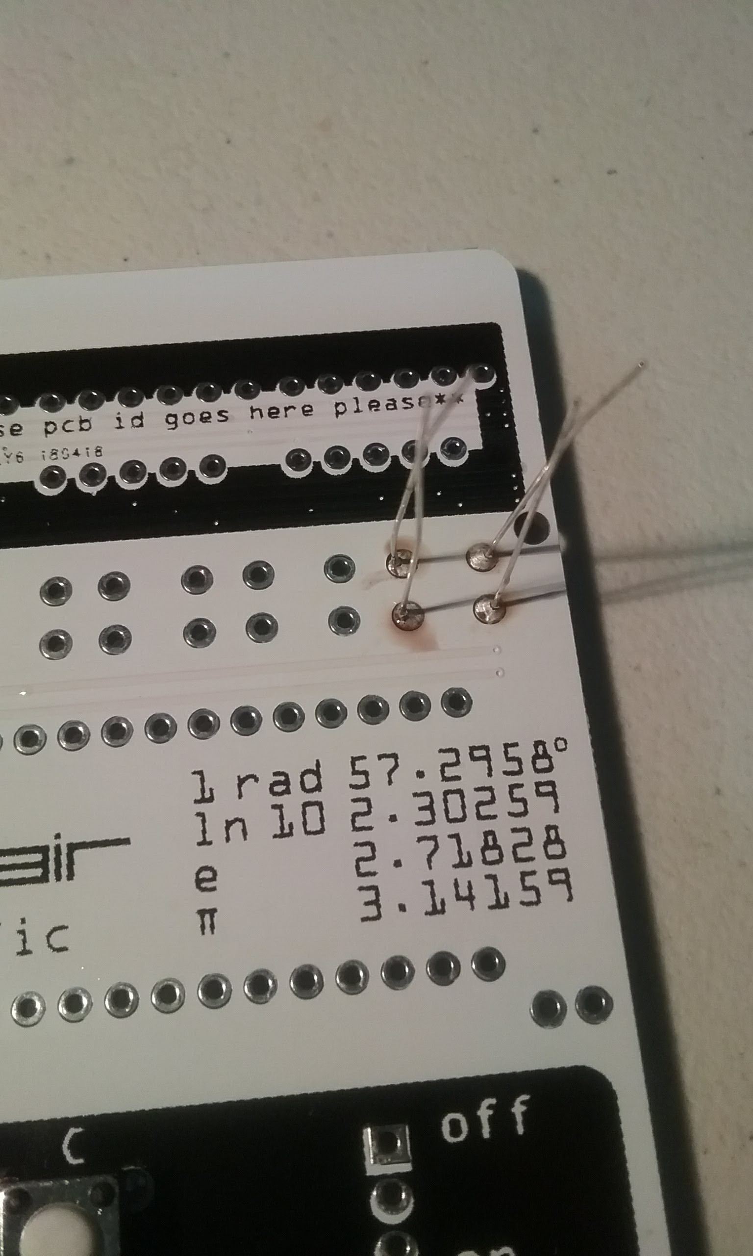
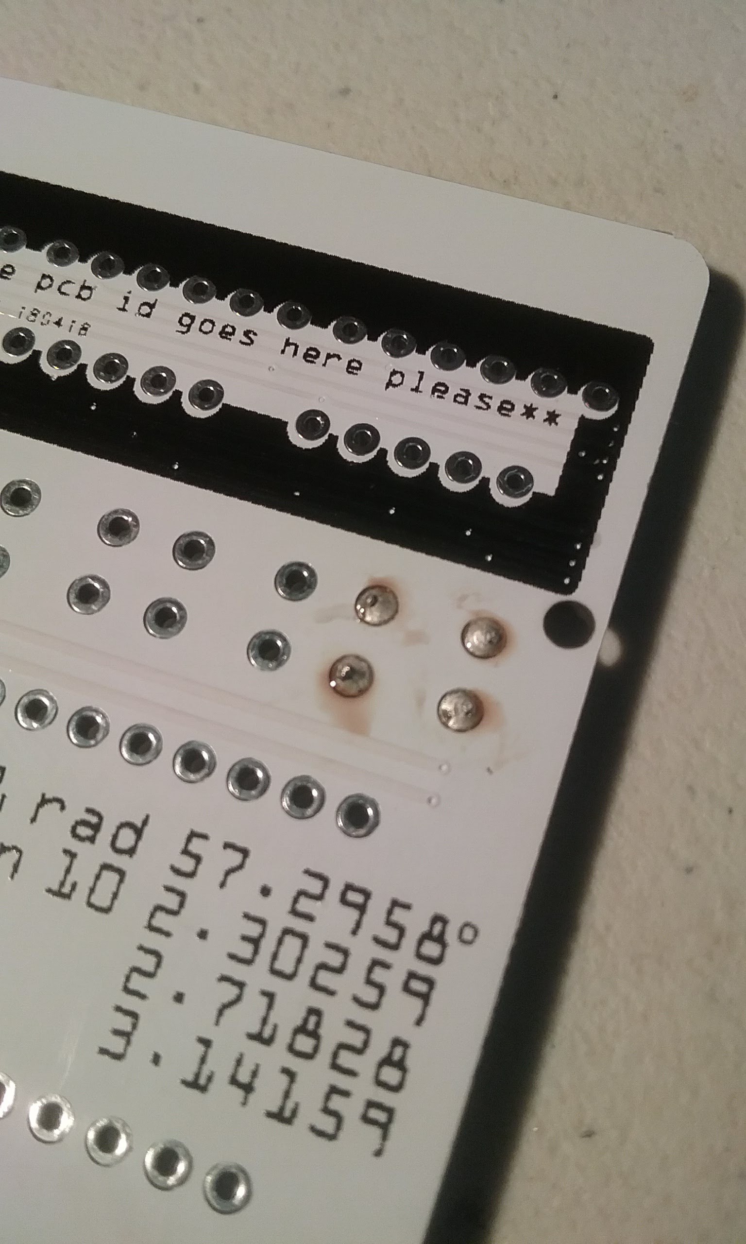
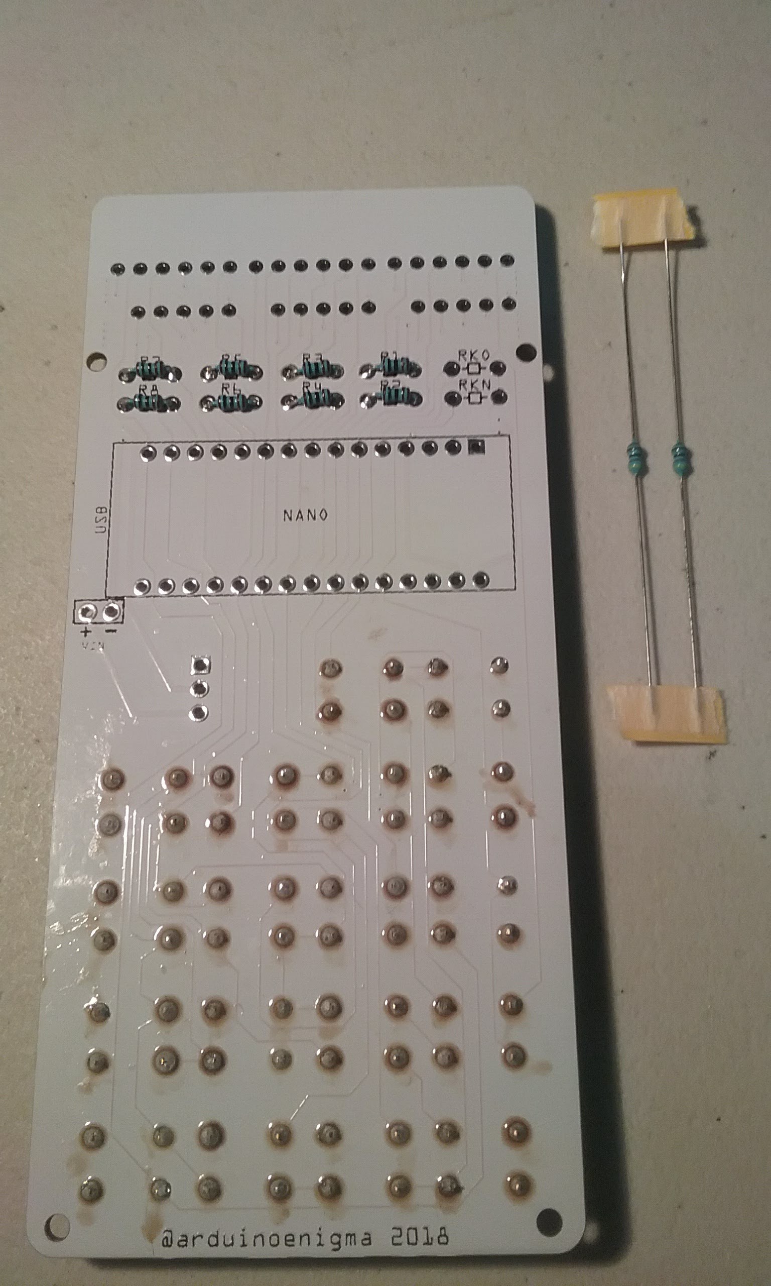
    Next, lets put the 4.7K resistors on RKO and RKN. These are weak pull down resistors and could be substituted with another high value resistor.

    The 4.7K resistors have a yellow line on one end.

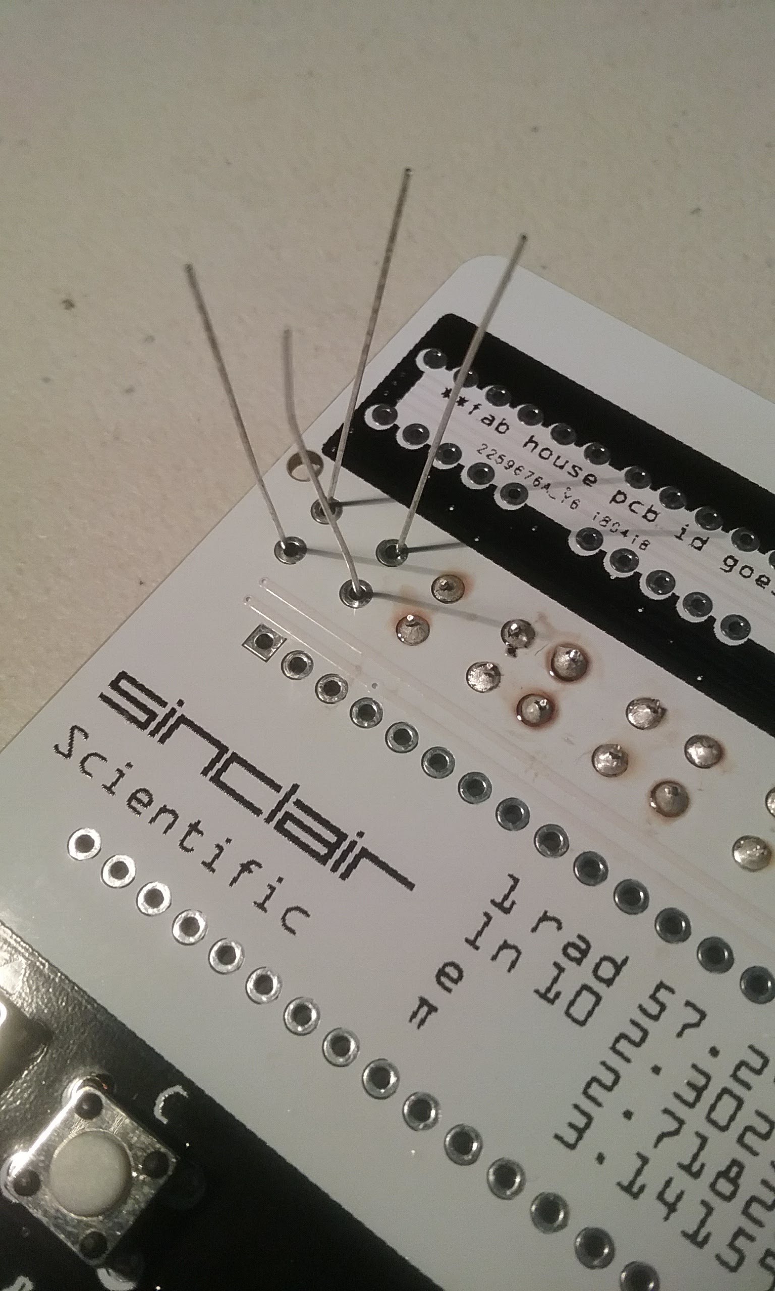
    Bend the legs and insert them through the bottom of the PCB.

    Solder and trim. By now all the keys and all the current limiting resistors should be soldered. The top of the board should look like this:

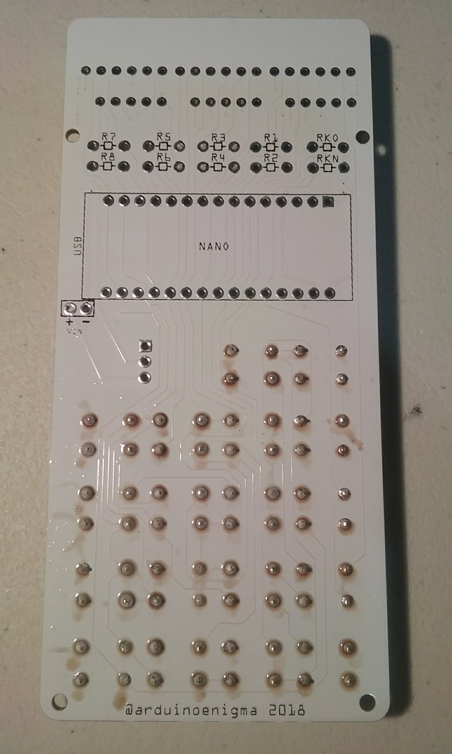
    And here is the bottom of the board at this stage:

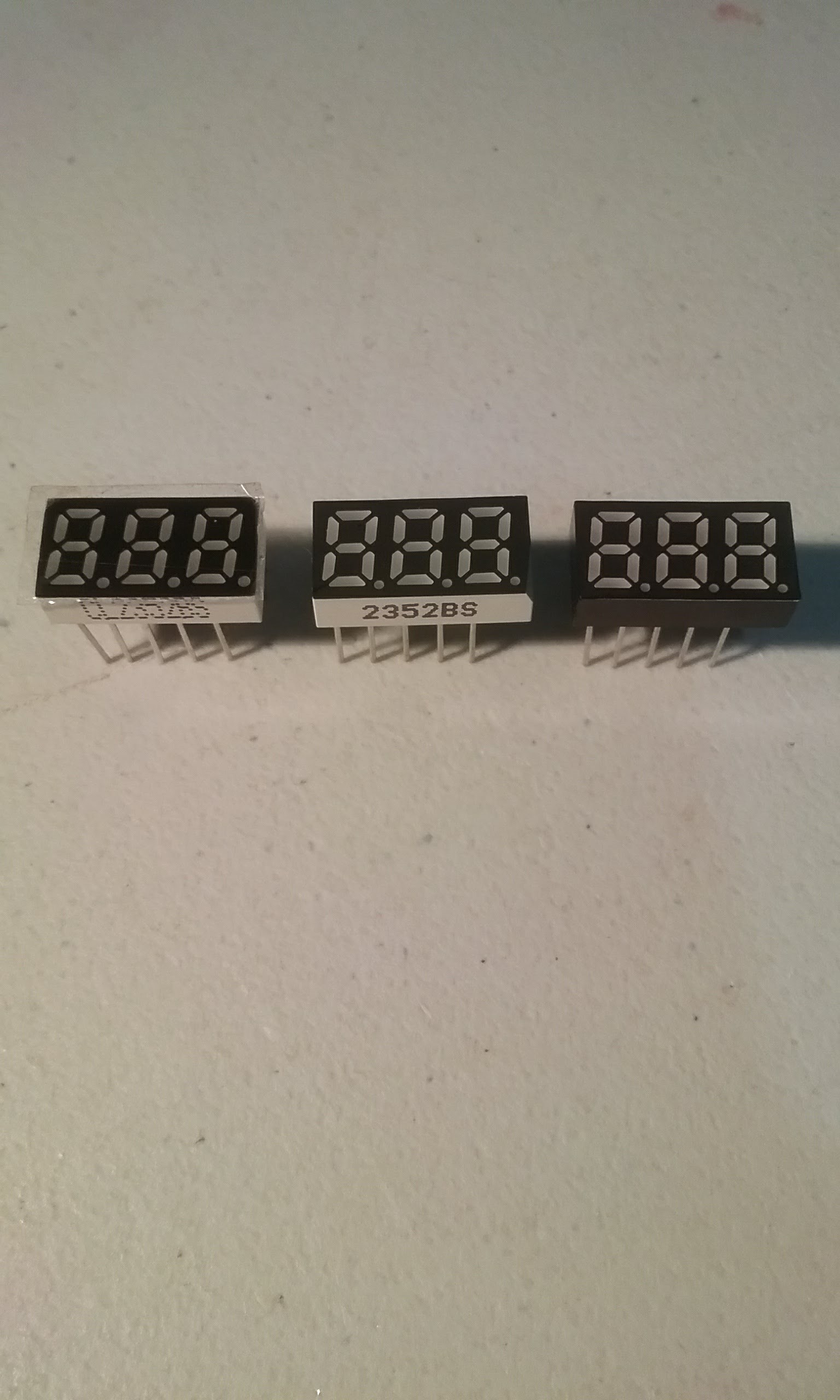
    Next we will prepare the displays. They come with a plastic film over the top. It can be pulled, as it is bigger than the display. Next, using a Permanent Marker, make the sides of the display black.

    Using the Permanent Marker, color the following space in the PCB. This will prevent the white soldermask to show in between the displays.

    Next, insert the displays on the PCB. They are keyed and only go in one way.

    This is how it how the bottom of the board should look like at this point.

    ... Read more »

  • A brief demonstration of this project's hackability

    Arduino Enigma04/24/2018 at 03:06 0 comments

    This was done on a dare by @davedarko , to add KITT as an easter egg to this emulator. Can you find the key sequence to activate it? It can only be displayed before the calculator software starts running.

    https://github.com/arduinoenigma/ArduinoNanoSinclairScientificCalculator

  • Reverse Engineering the keyboard and display circuit on a real Sinclair Scientific

    Arduino Enigma04/18/2018 at 02:31 0 comments

    By now the Black and White V2 PCBs have arrived. They are certainly slimmer than the V1 Green PCBs,

    One is quickly assembled. It starts to resemble the original calculator.

    A side effect of the pin assignment is that all 4 LEDs in the back of the Arduino Nano are lit up (D0,D1,D13,Power). This makes a fantastic backlight or ground effect. But I digress,

    The main problem with this board is that at its heart, it is still a KIM-1 circuit. Press two keys together and the same segment in all of the digits is affected. 

    Pressing two keys in the original calculator, instead corrupts the value displayed in two number positions, but the segments do not go dim like on the KIM.

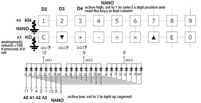
    On the online simulator, the red line moves to each digit and if the key is pressed, the top horizontal line (KN) lights up, if a function key is pressed, the bottom horizontal line (KO) lights up. If pressing two keys affects two digits, it means that the column selection lines are connected to the common anode of the displays.

    In the example below, if 5 and 7 are pressed simultaneously, if the 5 column is being scanned, the display connected to the 5th and 7th columns will be activated. Once the active selection line reaches the 7th column, the 5th column will be activated as well.

    We go back to http://righto.com/sinclair and ponder things for a while. Its funny how one can see things a few times and not realize what is going on. This calculator has a screen with 9 digits, counting the two positions where a minus sign is displayed. The keys are arranged in 9 columns. There is a counter in the CPU.ino file that rotates an active bit in an array. This means that the dActive / d is used as a strobe to select the digit to light up and activate a keyboard column to read. 

    void updateD()
    {
      for (signed char i = 10; i >= 0; i--)
      {
        SinclairData.d[i] = 1;
      }
    
      SinclairData.dActive += 1;
      if (SinclairData.dActive > 10)
      {
        SinclairData.dActive = 1;
      }
      SinclairData.d[SinclairData.dActive - 1] = 0;
    }

     While typing this, I realized that the Active value in SinclairData.d[ ] array is a 0 That means that the display in the Sinclair Scientific is a Common Cathode model. Our display is Common Anode. This only affects the polarity of the signals to make a segment light up and the value read at KN and KO, but that is a topic for another day.

    The key realization here is that the vertical lines are connected to the common anode pins of the displays. That way, every time the CPU step function is called, a column is selected. The value that's on the pins connected to the LED segments lights up on the selected position. If a key is pressed, it can be read on the KN or KO pins.

    The main difference with this circuit is that the KN and KO pins are always input, instead of the KIM Uno circuit where the LED segment pins are switched from output to input for a moment to read the keyboard. This immediately presents an opportunity to use the input only A6 and A7 pins that went unused in the V1 PCB. Since A6 and A7 are analog input pins, they must be connected either to 5V or ground to get a default value when a key is not pressed. Since the vertical selection lines are active high, and will put 5V on the horizontal lines when a key is pressed, the KN and KO pins must be connected to ground via a resistor. The schematic starts looking like this: 

    One thing that the schematic does not tell us is the order of the vertical selection lines. In the online emulator, they are arranged in numeric order, but that does not mean it is right.

    ... Read more »

  • How to design a custom PCB shape for Fritzing. No more sharp corners.

    Arduino Enigma04/18/2018 at 02:30 1 comment

    This guide will show the steps to create a custom PCB shape that can be used in Fritzing. In this case, the shape will be a rectangle with 3mm radius corners. This is enough to not have sharp corners, but not so big that it takes away from the usable PCB area.

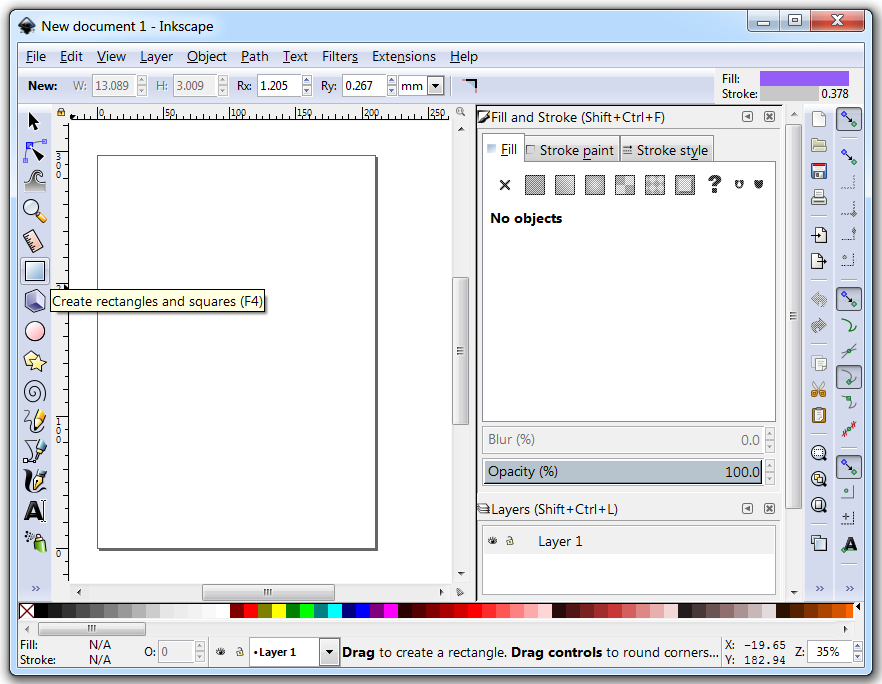
    First, launch Inkscape:

    if you don't have it, download it at: https://inkscape.org/en/release/ 

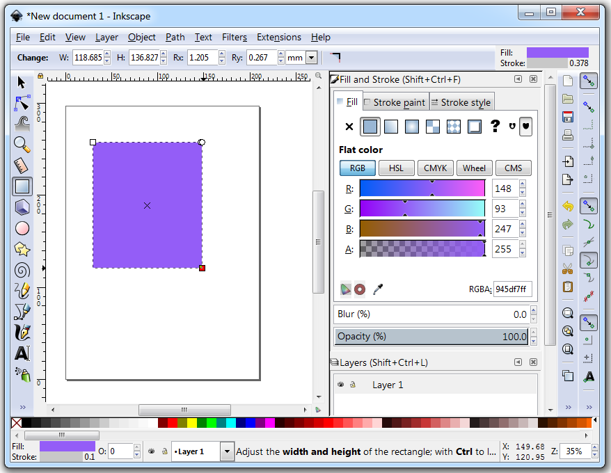
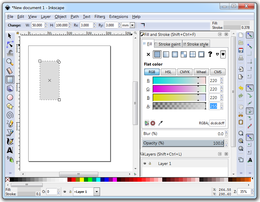
    Then click on the Rectangle Tool on the left and draw a rectangle by dragging the mouse. At this point the size is not important. The precise dimensions will be entered in the next step.

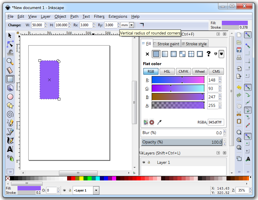
    While the rectangle is still selected, enter its dimensions in the boxes above the drawing area. We will make it a 50x100mm rectangle with 3mm radius corners.

    You will be staring at this rectangle for hours. So you can keep the rectangle this nice purple or select a color that's easy on the eyes. To do that, go to the Fill and Stroke window and use the sliders to select the desired color. I made them the same value to get a light grey. Leave the Alpha value (opacity) as 255.

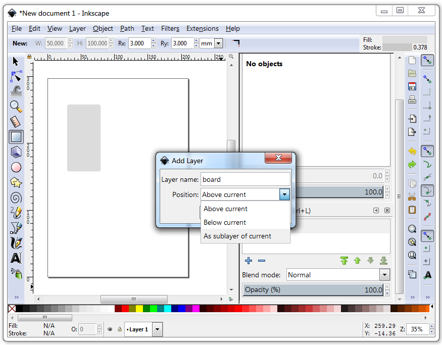
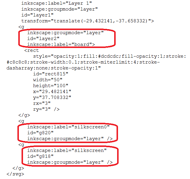
    Now its time to add three layers under the current layer.  Start by adding one as a sublayer of the current one, name it "board". These are only the visible names. Fritzing needs the layer ID to be named board, silkscreen and silkscreen0. I have not found a way to edit that in Inkscape, so this will be fixed later using Wordpad (or Notepad++ if you prefer).

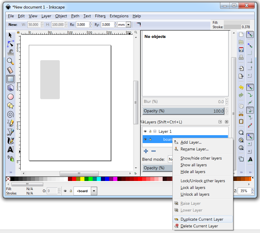
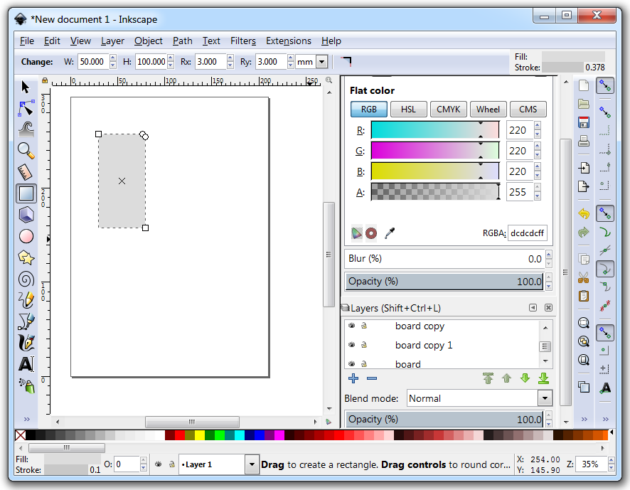
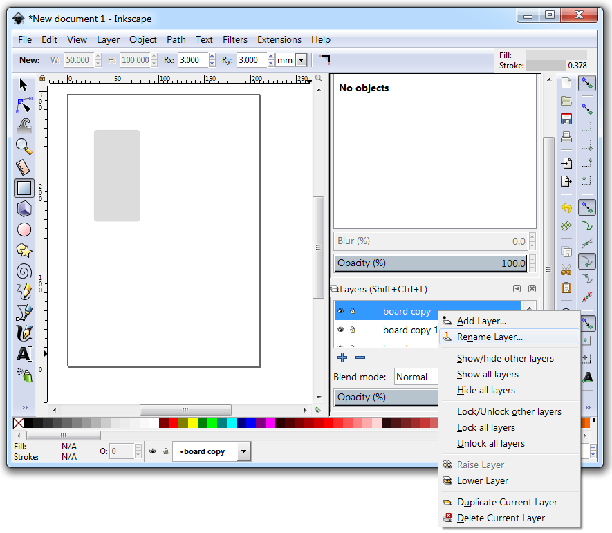
    Then, to create the other two, right click the layer named "board" and select Duplicate Current Layer. Do this two times.

    And this is how the layers will look like when done duplicating them.

    Now right click the copies and rename them silkscreen and silkscreen0

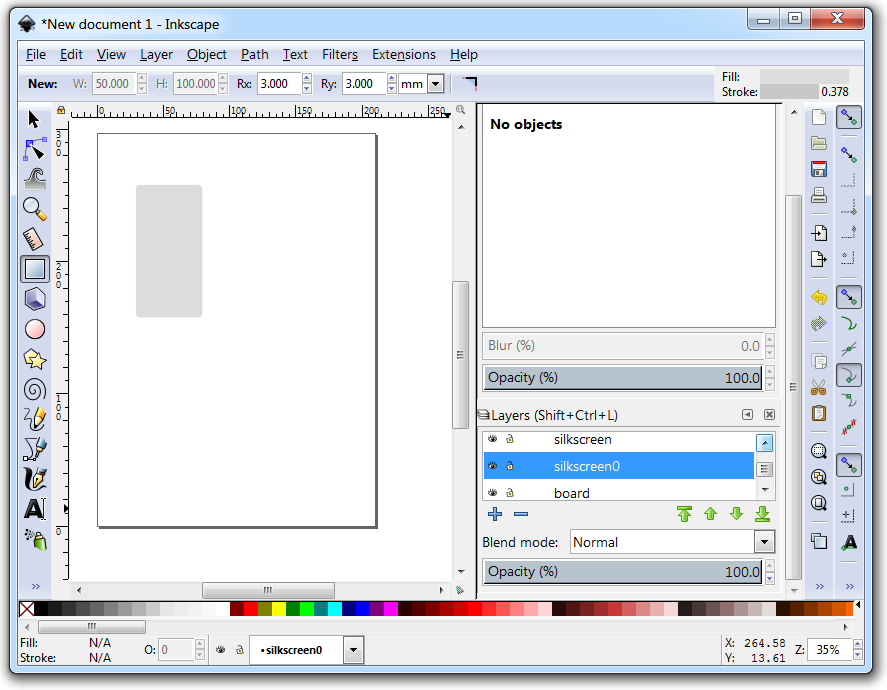
    And this is the final state of the layers:

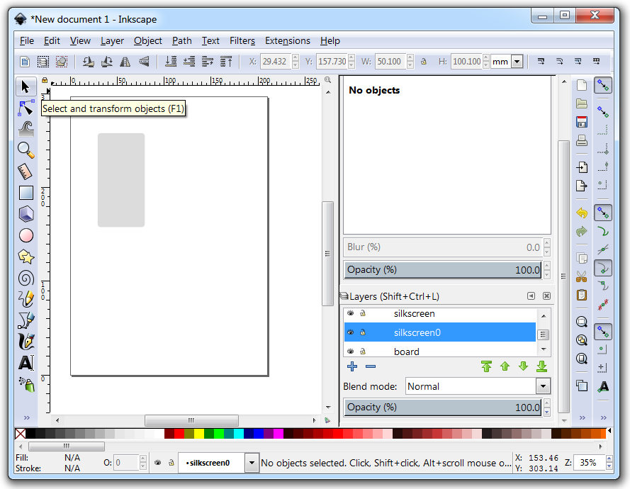
    Now, let's move the rectangle to the "board" layer. To do that, click on the Select and Transform Objects tool.

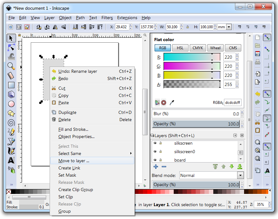
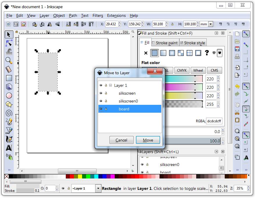
    Then click on the rectangle to select it and then right click it. Select Move to Layer...

    Select the "board" layer to move the rectangle there...

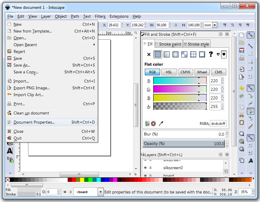
    Just one more step before we are done with Inkscape, let's trim the page to the size of the board. To do that, go to File -> Document Properties.

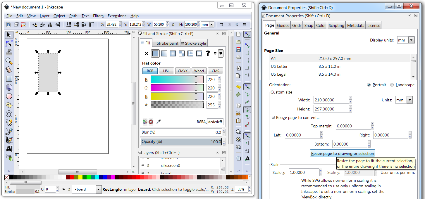
    And click on Resize Page to Drawing or section

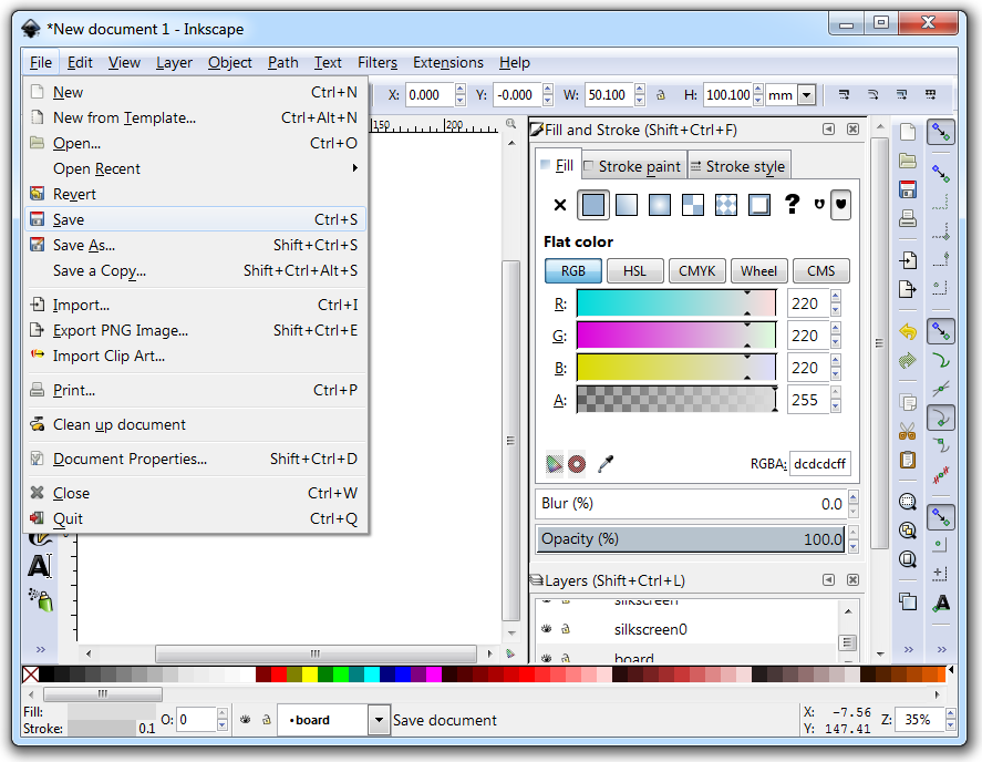
    Once the page is shrunk to the size of the rectangle, save the file. 

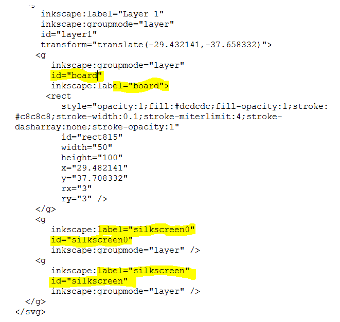
    The file, as created by Inkscape, will not work in Fritzing. This is because the layer id property is not set to the names Fritzing expects. The names that we set in Inkscape end up in the label property.  I have not found a way to fix this except for editing the file in Wordpad (do not use Notepad as the file does not use the CR LF it expects).

    To fix this, once the file is opened in Wordpad, copy the contents of the label property to the id property, as highlighted below.

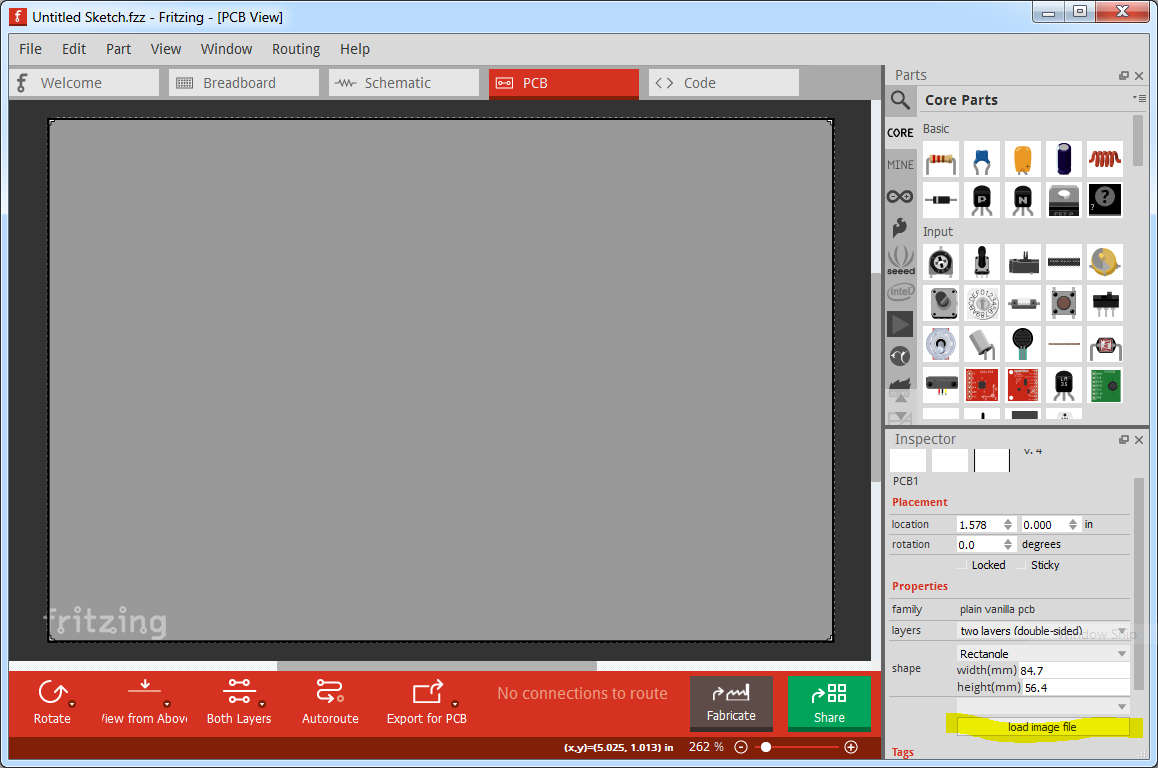
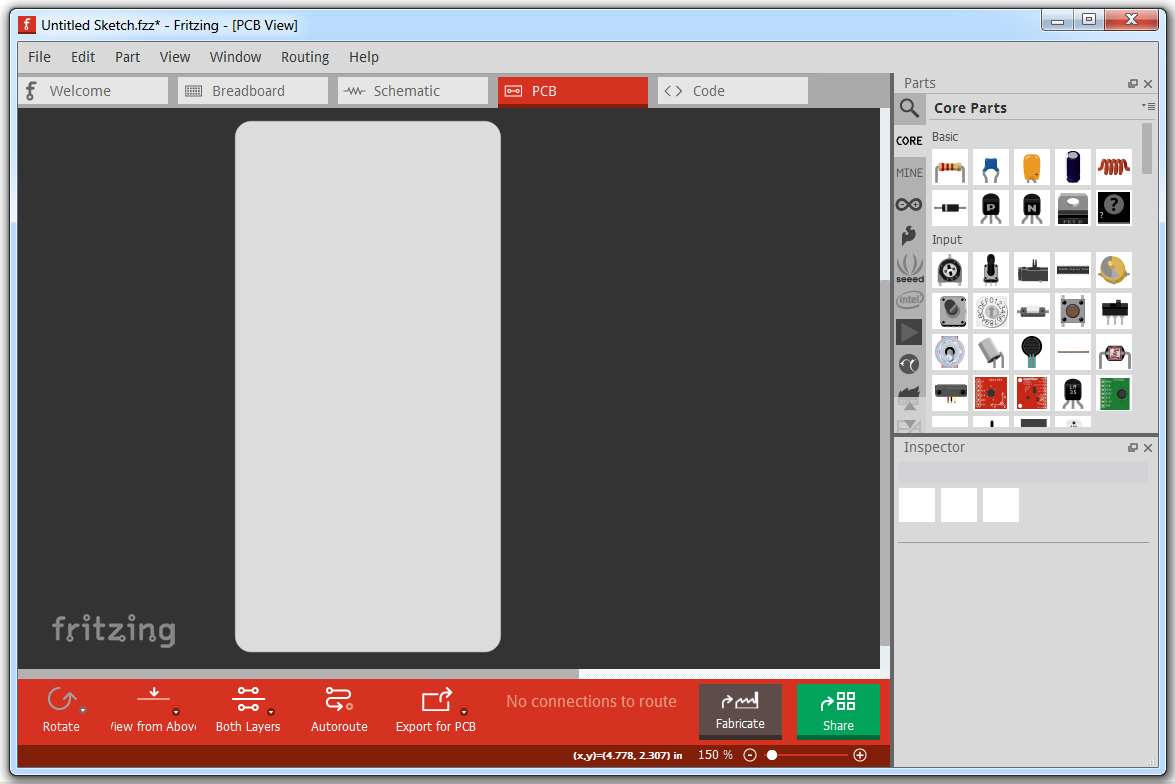
    Save the file and launch Fritzing. Click on the PCB and on the inspector window, click on the Load Image File button. Select the SVG file we have been working on.

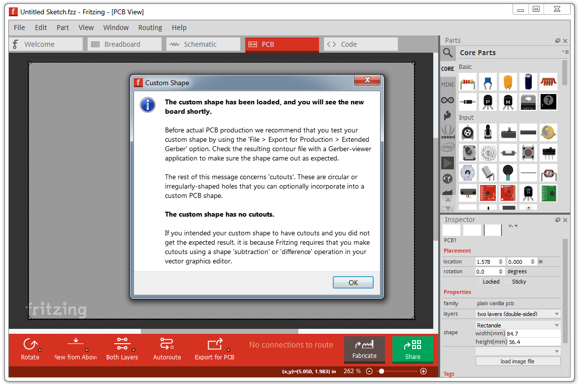
    Once Fritzing loads the custom shape it will show the window below. If another window complaining about the lack of a board or a silkscreen appears, go back and double check your work.

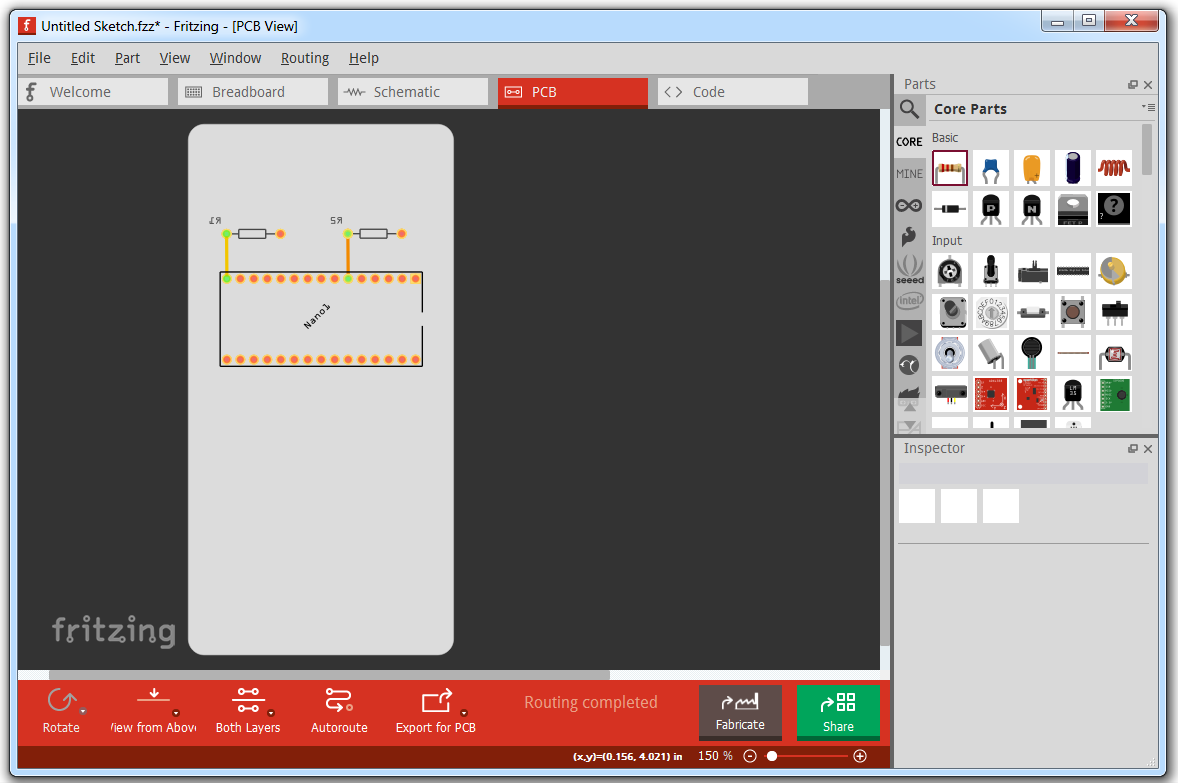
    And finally, here is the custom shape loaded in Fritzing, time to place components. 

    An Arduino Nano was placed as a sanity check to verify our dimensions (50mm width x 100mm height) are correct.

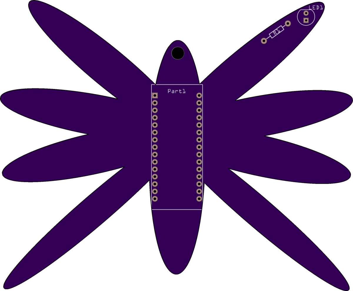
    And this is it, If you can draw it, it can be a PCB shape. The shape below was drawn as a series of ovals that were copied, pasted and mirrored, then joined using Union. This unfortunately will not manufacture correctly because the routing bit that will shape it cannot make that sharp bend. 

    Check out this cool...

    Read more »

  • 02/17/2018 - (some) Display Glitches emulated

    Arduino Enigma04/13/2018 at 23:07 0 comments

    I have been able to play with the real Sinclair for a few days now and have been able to time some instructions and notice some glitches.

    The following glitches have been coded in the emulator:

    1) When the calculator is busy, the display is off and the decimal point stays lit. The decimal point gets brighter than normal when the rest of the digits are off. This results in an interesting effect when a simple operation, like addition is performed. The display blinks briefly, and the dot flashes briefly. 

    2) When numeric keys are being pressed, the first digit in the display seems to count quickly through all the digits before returning through its previous value. When a 1 is shown, it looks like an 8 or a 0 is briefly flashed. 

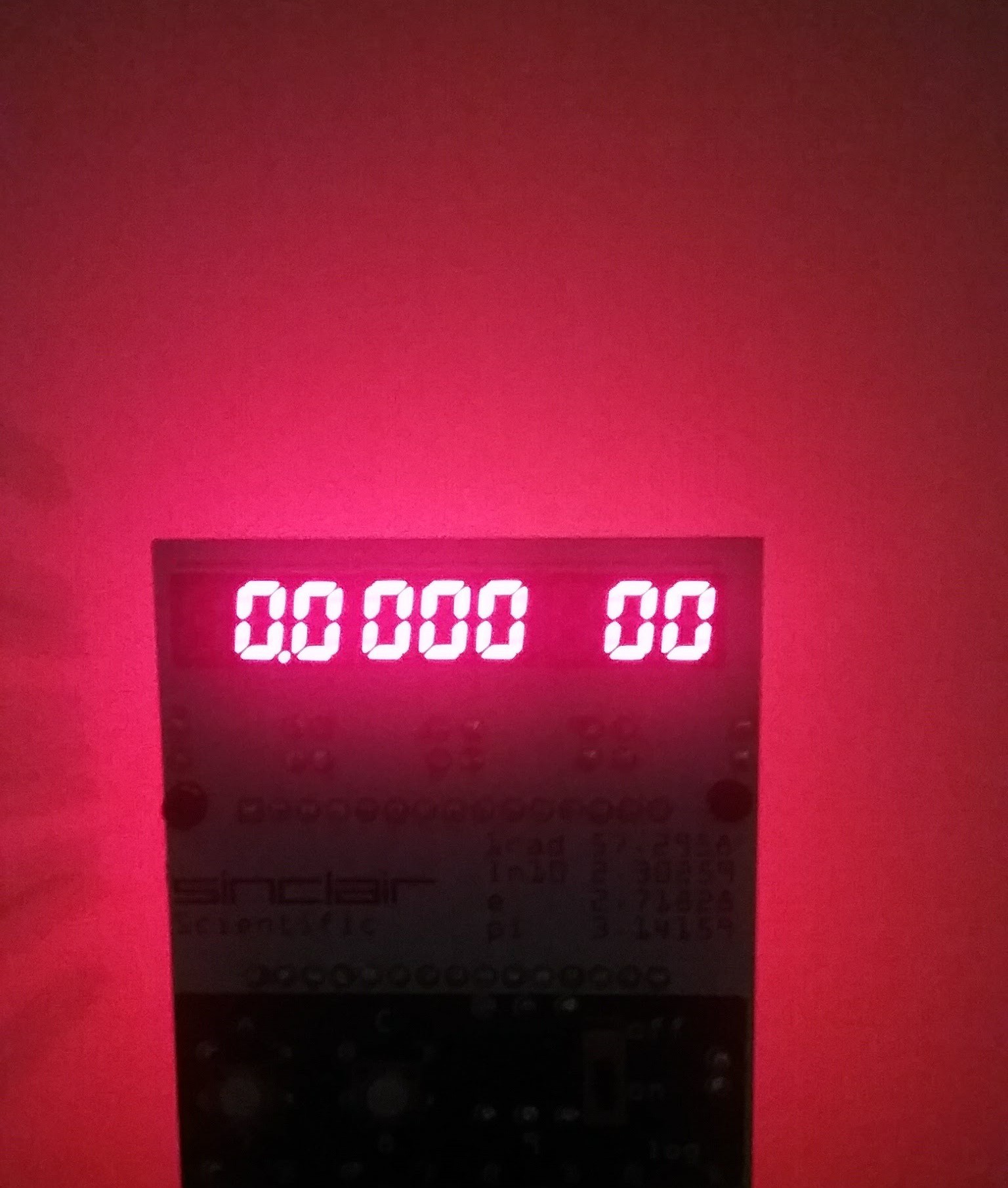
    3) Pressing the C key makes the display get a little dimmer than normal. The C key is an interesting one. It is wired to the CPU, but the code does not do anything with it. Somehow it performs a hardware reset. We simulate that in software by setting the program counter to 0 and then letting the first 8 instructions execute. This clears the A register, resulting in 00000 00 being shown on the screen.

    The instruction timing issue has been resolved by having the step() function take a fixed amount of time to execute regardless of which instruction runs.  The snippet below shows that the current time in microseconds is measured at the start and the end of the function. The execution time is measured and if it is less than a certain value, the difference is computed and we delay for the desired amount. Looking at the code below, the line where the subtraction is performed would probably be better prior to the IF statement so it always executes. Another way to solve this problem is to make steptime larger than needed, so this subtraction is always performed. 

    The execution time was determined by comparing exectime with maxexectime  and outputing exectime if it was greater than the previous maxexectime. This code was deleted once it was determined that the slowest instruction took 145uS to execute. The initialization code sets steptime to 148 when the program starts. When the C key is pressed, steptime is reduced so the step() function executes faster and a smaller digit refresh delay makes the display dimmer. 

    void step()
    {
     ...
    
     unsigned long entrytime = micros();
    
     ...
     switch (opcode)
        {
          case 0: // AABA: A+B -> A
            displayInstruction(1);
            add(SinclairData.a, SinclairData.b, SinclairData.a);
            break;
          case 1: // AAKA: A+K -> A
    
     ...
     byte exectime = micros() - entrytime;
    
     if (exectime < SinclairData.steptime)
     {
       delayMicroseconds(SinclairData.steptime - exectime);
     }
    }

     All the V1 PCBs are assembled and the green wire fixes done in wirewrap under the Arduino Nano. They are listed in our Tindie Store in an attempt to recoup some of the costs of purchasing the original calculators, the PCB and the supplies needed to assemble this.

    Time for a quick instagram post:

    https://www.instagram.com/p/BfUR9a8Hs0i/

    This project will be on hold for a few weeks while working on this big insanity, 367 switches 

    https://hackaday.io/project/78869-smaller-simone-giertzs-good-habit-tracker

  • 02/08/2018 - Original Sinclair calculators arrive!

    Arduino Enigma04/13/2018 at 18:05 0 comments

    And a couple of orders from eBay arrive.

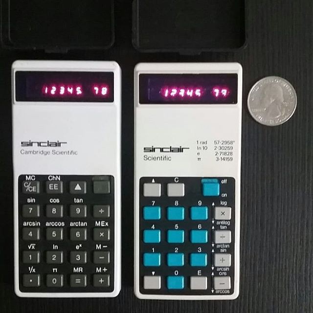
    The one on the left was an impulse purchase.... It is a much better calculator, more accurate, faster, uses only 2 AAA batteries. No online simulators or other information on the chip though...

    These things are tiny! Its hard to explain the feeling of holding one in your hands. A picture with a quarter, like Sparkfun used to do, is taken for scale.

    In retrospect, this purchase was a good decision. To make a good simulator, it helps to have access to the original item. 

    Playing with the calculator, I start to notice all sort of normal little display glitches. The biggest find yet is that when the calculator is computing a result, the display goes blank AND the decimal point stays on. The emulator is immediately modified to account for this.

    Now I can see how long different operations take and adjust the refresh display delay to try to match the emulator speed. Problem is if I adjust the delay to match the arccos, the arctan speed is off. I begin to suspect this has something to do with the speed at which the emulated CPU instructions execute. Simpler instructions take less time to run. I start thinking of a way to make all CPU instructions take the same time to execute...

    Time for a couple of quick tweets:

    https://twitter.com/arduinoenigma/status/961762438365569025

    https://twitter.com/arduinoenigma/status/961765858304581632

    https://twitter.com/arduinoenigma/status/961857709925482498

  • 01/23/2018 - Slimmer Black and White V2 Board sent to production

    Arduino Enigma04/13/2018 at 18:01 0 comments

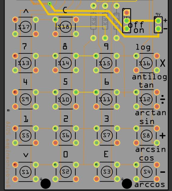
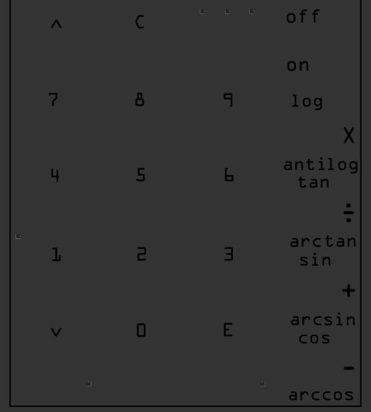
    It is becoming evident that V1 is a little too wide. The PCB is cut to the width of the resistors, the power plug is moved inwards and the scientific function labels are moved above and below the keys. For this board, a keyboard mask is created. The board will be ordered with white soldermask and black silkscreen to resemble the calculator. 

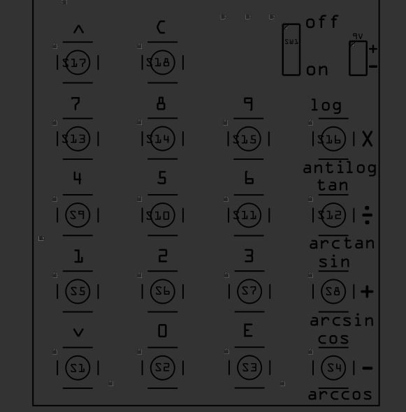
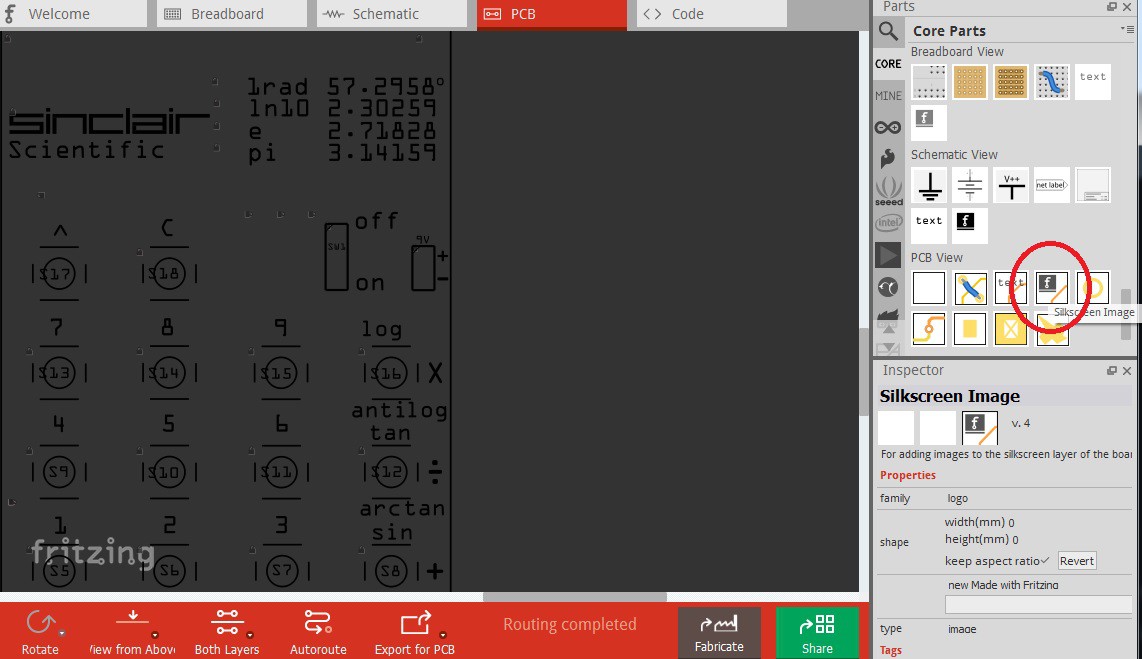
    Here is a picture of the layout. What follows below are the instructions on how to create a negative mask using Fritzing, the Sniping Tool and Paint.

    First, design the layout of the labels to appear. Don't worry too much about final location, labels can be moved and deleted later. Just make sure all the labels you want are drawn at this point. 

    Then, turn all the layers off View->Hide All Layers and then turn on only the top silkscreen View->Silkscreen Top Layer

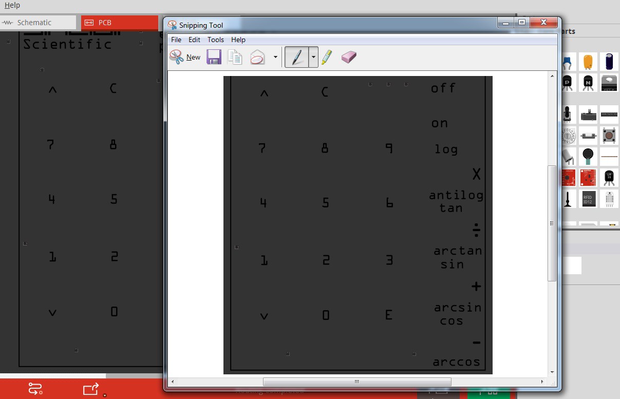
    To help the cleaning process later, the buttons can be deleted at this stage. Just make sure to save the file first and then revert to the saved file. The goal of this step is to minimize the amount of editing in Paint. A few stray marks are ok, they can be deleted later.

    Then, using the Sniping Tool, capture the keyboard area.

    Without saving anything, go to Paint and select Paste (Ctrl+V)

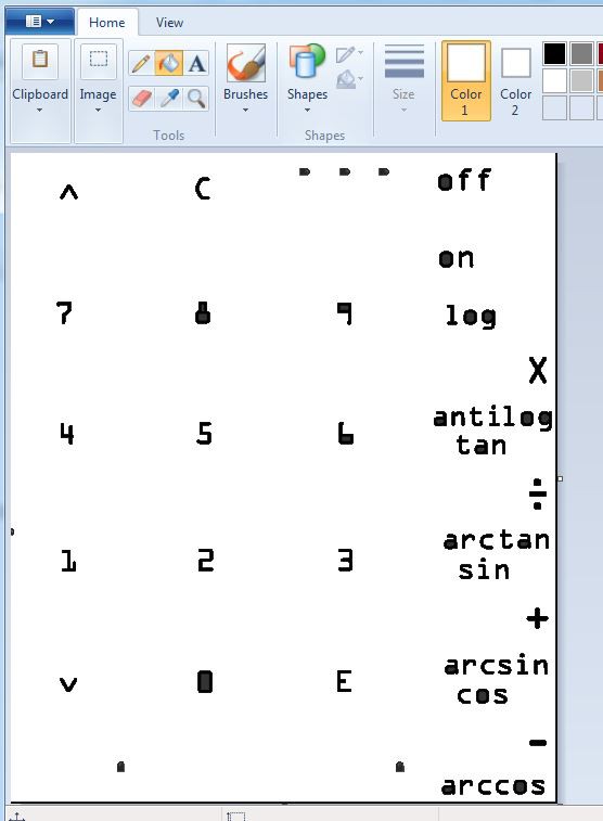
    Click on Color 1 and click on White. Then click the Bucket Tool and click on an empty area of the picture to paint it white.

    Zoom in  and paint inside any closed letters. Any undesired marks can be deleted at this step as well with the Eraser tool.

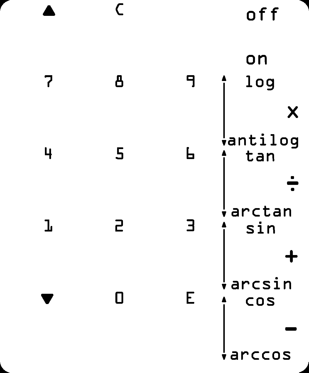
    Rounded corners and any desired artwork can be added at this step. The location of the text labels can be fine tuned also. If you want to add a logo like the OSHW gear, do it now.

    When ready, save as PNG, if the file is saved by mistake as a JPG, compression artifacts will be visible when imported into Fritzing. If this happens, go back, press (Ctrl+Z) to undo a couple of steps, save as PNG and redo the last couple of fixes that were undone.

    If the file is saved as PNG, a lossless format, it will look nice and clean when imported into Fritzing.

    To import the keyboard mask into Fritzing, go th the Core Parts bin and drag a Silkscreen Image into the PCB view.

    Then load the file we have been working on. To do that, go to the Inspector window and click the button above "image"

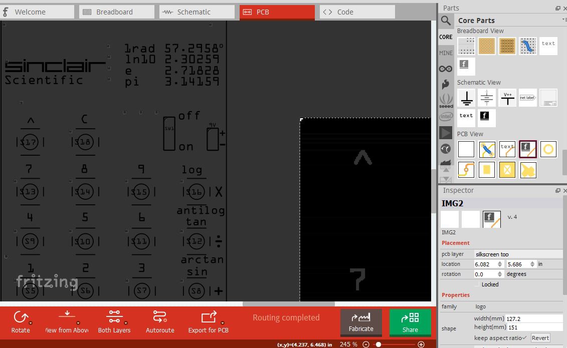
    The image has been imported at its native DPI, to make it wit, set approximate width and x-y location. A good initial width is one a little less than the PCB, 49mm.

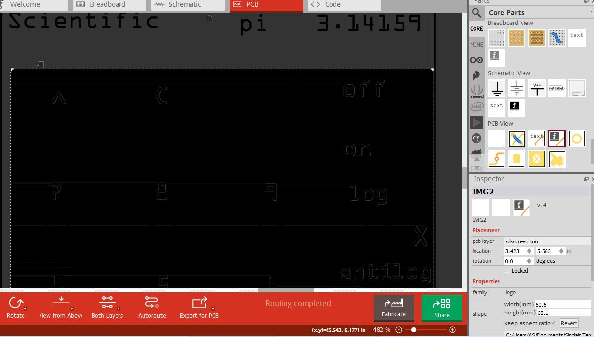
    Then align the character on the top left corner so the hole in the image and the silkscreen image overlap. Notice that towards the right, the labels do not align. Its time to fix that by finding the exact image width to use.

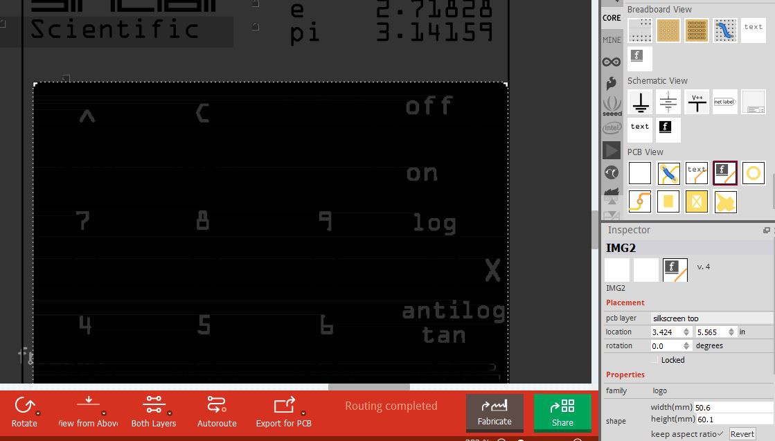
    Trial and error yields 50.6 as the value that makes all the labels align. The image can be repositioned to make sure the top left label still fits well. 

    Note the x and y location values and move the image out of the way. Now its time to delete the silkscreen labels that were above the components. 

    Finally, move the image back to the previous location. There are no visual clues as to what is the desired location, that's why we noted them on the previous step.

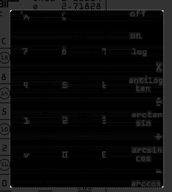
    Finally, to verify that the alignment is correct, turn all the layers back on. Select the Bottom Layer as clickable and select View from Above. Any issues with the size of the image can be resolved by editing the file in Paint. 

    To make the image appear narrower without affecting its true width or calculated location, go to Paint and add a black line on the right and save it (as...

    Read more »

  • 01/19/2018 - Figured out some details about the real calculator.

    Arduino Enigma04/13/2018 at 06:39 0 comments

    So far, I had been using Ken Shirriff's simulator (http://righto.com/sinclair) and things were matching. Trawling through instagram, I find a person that owns a Sinclair Scientific. I ask him to post a video of a calculation being performed and he graciously does it.

    https://www.instagram.com/p/BeFLrVTH424/

    I realize three things: 

    1) The display goes blank when computing a result. (at the time I did not notice in the video that the decimal point stays on and did not implement that)

    2) The emulator was running faster than the real calculator.

    3) If I am serious about this project, I must get my hands into an original Sinclair Scientific. Asking people on the internet to post videos is not going to cut it. The search on ebay has been started already. 

    Items 1 and 2 are partially corrected and a video is taken:

    Time for a quick instagram post:

    https://www.instagram.com/p/BeHoAe9HI-3/

View all 23 project logs

  • 1
    Build the keyboard

    On the front side of the board, install the blue pushbuttons on the number keys and the white pushbuttons on the rest of the keys. Flip the board over and while putting pressure to ensure all the buttons stay fully inserted, solder the whole keyboard.

  • 2
    Solder the resistors

    On the back side of the board, install the 8 LED display current limiting 1K resistors on the spaces labeled R1 through R8, just below the display.

    On the back side of the board, Install the keyboard 4.7K resistors on the spaces labeled KR1 through KR3.

    Flip the board over to the front and solder the resistors.

  • 3
    Install the LED displays

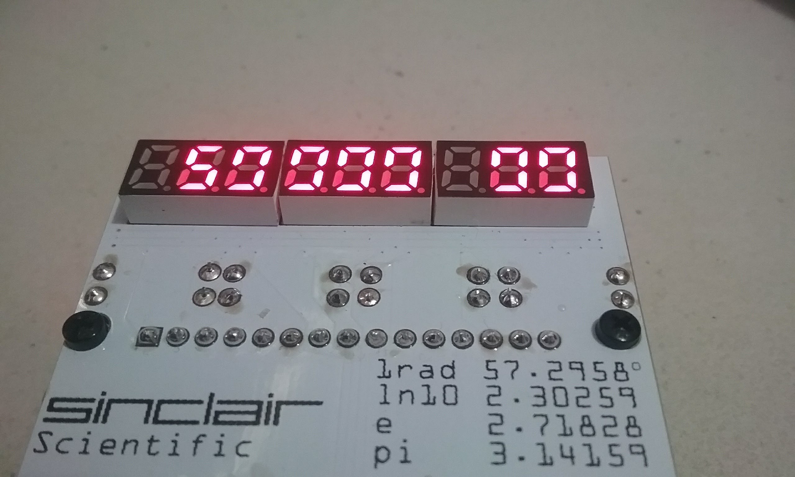
    Depending on the version of the board, the displays are placed too close together. To make them fit, sand down the b,c,d, and e sides of the displays. Consult the diagram below:

    [a DS1 b] [c DS2 d] [e DS3 f]

    Install them in the front, flip the board over and solder them.

View all 8 instructions

Enjoy this project?

Share

Discussions

Telly Spyropoulos wrote 06/03/2023 at 22:08 point

I have an issue with this one. I built the first one and it worked like a charm. Then I built a second one with the same exact parts for a friend. Everything works except the "1" key. The "1" does not register. Actually, it registers and blanks the screen to zeros, as if I had pressed CLEAR. I replaced the key with another one, traced some of the connections, but could not find anything wrong.

Any suggestions anyone?

Thanks,

Telly

  Are you sure? yes | no

Charles Syms wrote 03/10/2023 at 00:27 point

HELP, I cannot program the Arduino Nano, I get errors and it won't compile. I have tried many of the available sketches and they all won't compile. One error is "allSegmentsOff not defined"

Can someone please help me on the programming of the Nano?

Maybe can I but a pre-programmed Nano.

Charles

  Are you sure? yes | no

Telly Spyropoulos wrote 06/03/2023 at 22:06 point

Charles,

Did you get it to work? Are you using a real Nano? I had a hard time with a Nano clone. Did you install the AVR board library and selected "Arduino Nano" and processor ATMega328P?

Telly

  Are you sure? yes | no

zpekic wrote 11/13/2019 at 19:14 point

Super cool project! I was fascinated by the same device, check out my take on it :-)

  Are you sure? yes | no

Arduino Enigma wrote 11/14/2019 at 05:59 point
Awesome project! FPGAs are crazy!

  Are you sure? yes | no

shuford wrote 08/20/2018 at 02:13 point

The highest quality project that I have ever seen!  Just Brilliant workmanship & attention to detail.  Mind blowing documentation with a complete photographic record of all stages of the the project.  Arduino has probably put more work into developing the prototype than Clive Sinclair put into designing the whole original calculator!  A Tour De Force!  Job Well Done!

  Are you sure? yes | no

Vincent wrote 08/22/2018 at 22:53 point

Agree!

  Are you sure? yes | no

Ed S wrote 03/20/2018 at 07:47 point

An excellent project! And thanks for making the kit available.

  Are you sure? yes | no

Arduino Enigma wrote 03/21/2018 at 03:29 point
Thanks for the kind words, means a lot!
  Are you sure? yes | no

Similar Projects

Does this project spark your interest?

Become a member to follow this project and never miss any updates