Aleksa
-
PGA: Programmable Gain Amplifier
06/13/2021 at 01:09 • 0 commentsIf the FFE is the front of the front end, then what's in the rest of the front end? To complete the front end, this board needed finely adjustable gain, dc offset control, nyquist filtering, and an ADC driver. That sounded like a lot of work! Luckily enough, [bunnie & xobs'] probe schematics introduced me to just the right part for the job, the LMH6518 PGA. With adjustable gain from −1.16 dB to 38.8 dB, a whopping 900 MHz bandwidth, selectable bandwidth limit and 100Ω differential output, this chip had it all!
To use the input signal from the FFE with this chip, it had to be level shifted from +/-2.5V to 0-5V to fit within the PGA's positive voltage range. This was done by a pair of resistors (at the cost of a 2x attenuation!). DC offset control was accomplished by feeding a DAC output into one end of the PGA. This board also forced me to standardize on a connector series to use for the rest of the prototype. I ended up going with the FX18 series from Hirose, as they were compact (with a reasonably solder-able 0.8mm pitch), rated for high speeds, and had right-angle options that allowed me to connect everything in one plane.

The QFN package gave me some trouble and required rework later, but otherwise this board came together pretty well. I didn't want to continue on with the next board down the line without making sure this chip worked as expected, but probing that connector or its pins would be awful. And so we move on to the topic of the next post, making a front end tester board and testing the front end as a whole!
Thanks for giving this post a read, and feel free to write a comment if anything was unclear or explained poorly, so I can edit and improve the post to make things clearer!
-
The Front of the Front End - Part 2
06/07/2021 at 23:11 • 0 commentsNow that FFE Rev 1 was built, I had to test it to see if it met the lofty goals I set for it in my front end specs - 350MHz bandwidth, 1MΩ//15pF input impedance, 4 selectable attenuation ranges (0x,10x,100x,1000x), AC/DC coupling and switchable 50Ω termination.
*Spoiler Alert* It did not.
And that's fine, it was my first revision and that was pretty much to be expected. This log details how I tested it and the things I learned along the way!
Test Setup
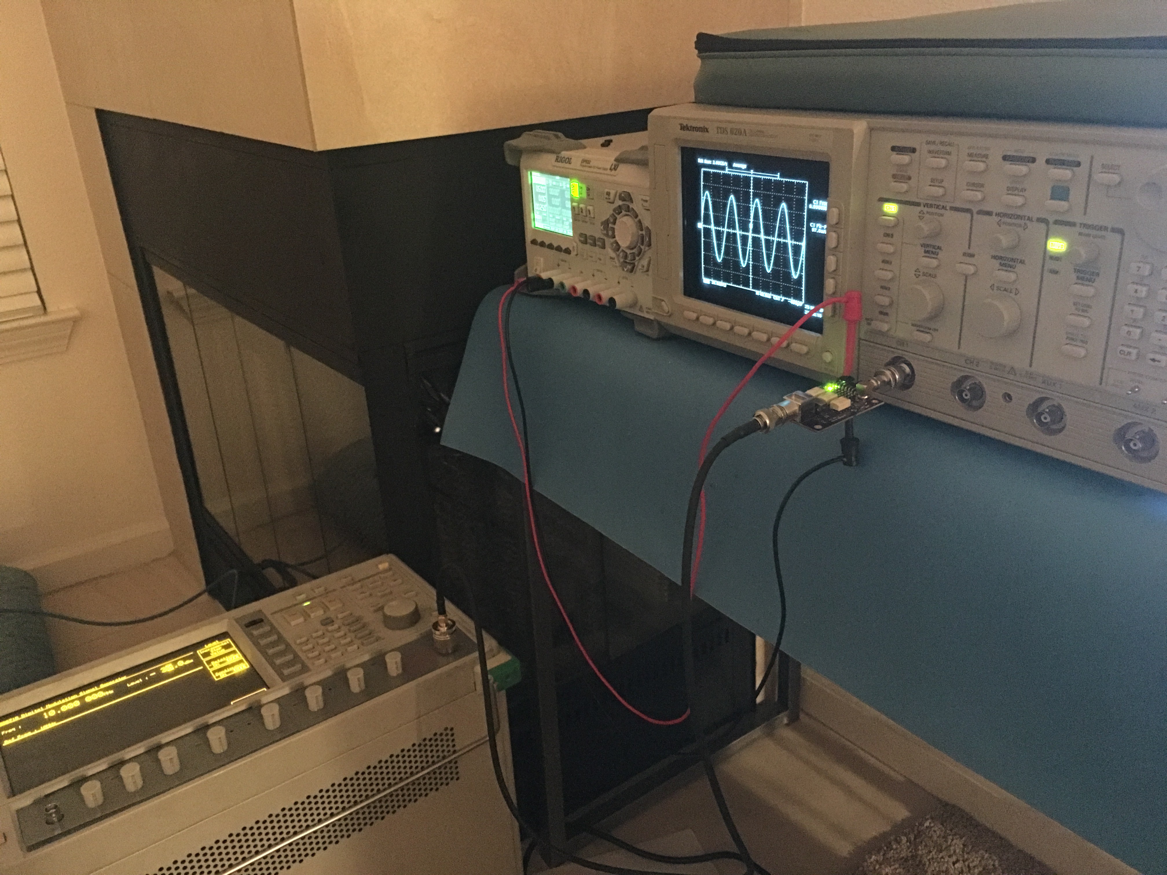
![]()
After annexing a corner of the living room (with apologies to my housemates), I set up a power supply, oscilloscope, and RF signal generator to start frequency response testing on the FFE board. I swept frequencies with the signal generator and recorded the average amplitude off of the oscilloscope. This got tedious very quickly, but I eventually automated it with a USB GPIB controller and PyVISA. GPIB is just about as old as dirt, but if you happen to have equally as old equipment, it's an absolute lifesaver.
![]()
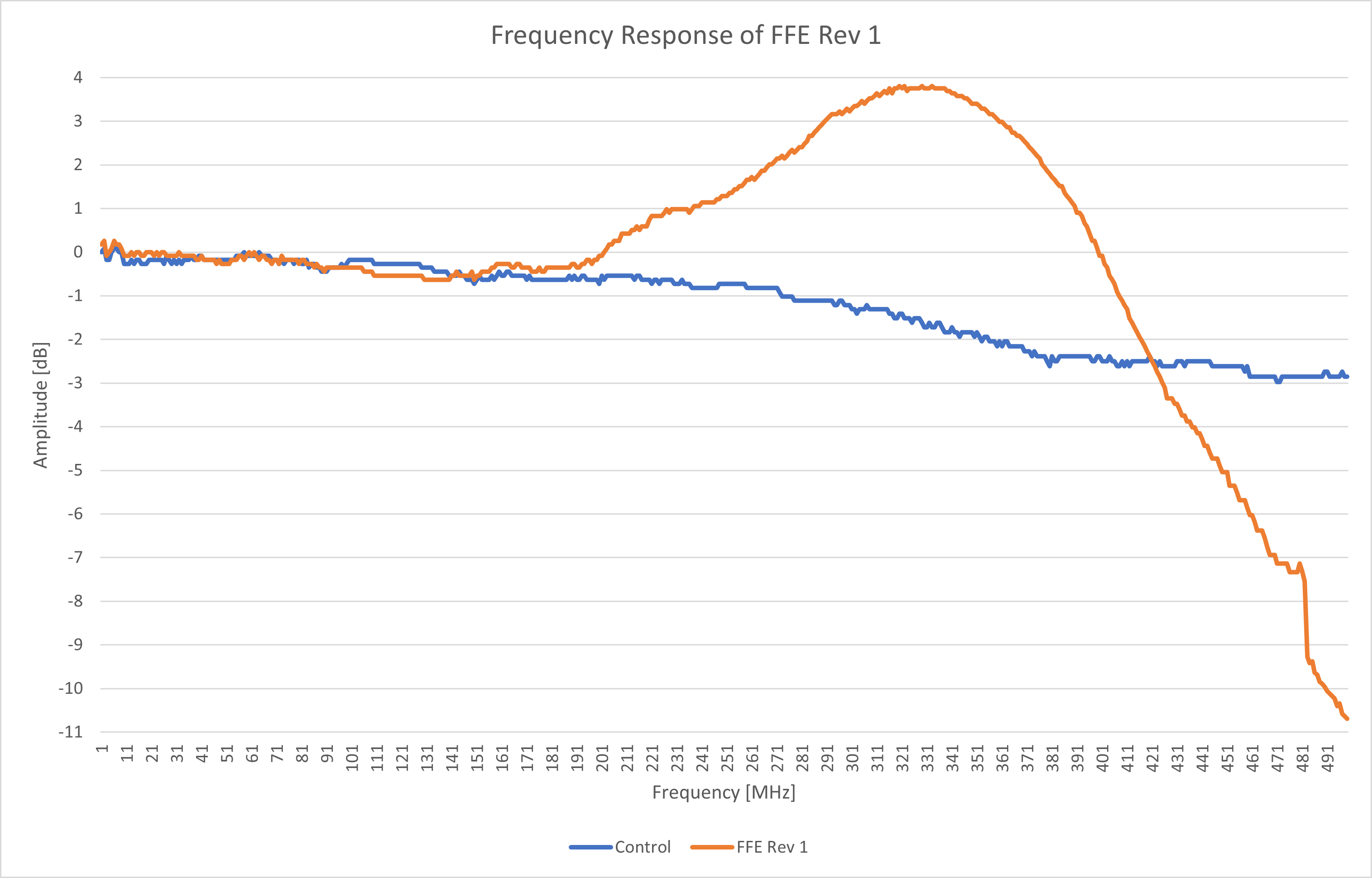
Here's the frequency response of FFE Rev 1 with the attenuators off, AC coupling on, and 50Ω termination enabled. The blue line is the frequency response of the oscilloscope doing the measurements to provide some sort of baseline for relative comparison (my equipment wasn't calibrated, so technically relative measurements are all they're capable of). Although the -3dB bandwidth was over 400MHz, there was massive (3db!) peaking past 200MHz. This wouldn't work for a front end. On top of that, the output oscillated from rail to rail when any of the the attenuators were enabled. The only good news was that it worked with regular scope probes.
![]()
The reason for the peaking eluded me at the time, though now I believe it was due to either the opamp's marginal stability at a gain of ten or the parasitic inductance and capacitance in the layout, perhaps even both. When filtered by the PGA's adjustable bandwidth limit (I would set it to 200MHz), I thought that the peaking would be acceptable enough to test the rest of the system until I made a new revision. As for the attenuators, switching them in massively increased the capacitance at the opamp input, which was probably the cause of the oscillation. I'd have to avoid using them whenever testing the system, which limited me to a select few voltage ranges.
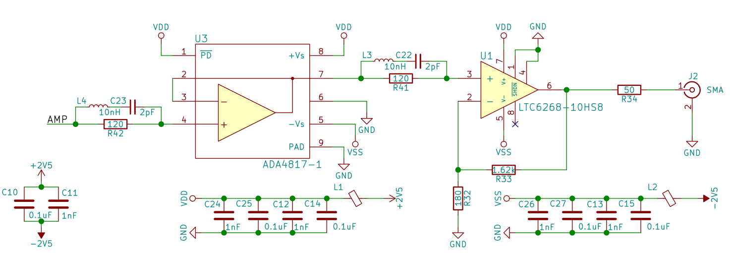
Rev 2It really bugged me to move on to designing the rest of the system while the FFE was still an absolute mess! Instead of scrapping the design and figuring out the fundamentals behind why it didn't work, I came up with a solution in a single afternoon (this had to be good right?). The idea was to take some of the pressure off of the main opamp, and add another one in front of it to better handle the changing capacitance when the attenuators switch.
I used the same ADA4817-1 opamp that [bunnie & xobs'] used in their oscilloscope probe, alongside the damping circuit (which they DID label as damping 1GHz peaks, so I figured tweaking the values would help me tame the mountainous peak at 340MHz). So in the same afternoon that I thought of this fix, I layed it out and sent it off to fab!
![]()
The only thing that's peaking here is the BOM cost with the extra opamp! Kidding aside, it was clear that the FFE was going to be very difficult to do right, and would need a complete overhaul for Rev 3. Until then, I would continue to build the rest of the system so that work on software could start, and then loop back and give the FFE the respect it's due.
Thanks for giving this post a read, and feel free to write a comment if anything was unclear or explained poorly, so I can edit and improve the post to make things clearer!
-
The Front of the Front End - Part 1
05/30/2021 at 21:03 • 0 commentsAn oscilloscope's input buffer has a very odd (and strict) set of requirements. Its input impedance must be 1MΩ in parallel with about 15pF, for compatibility with standard oscilloscope probes. The front end must also take in any signal within the oscilloscope's voltage ranges and attenuate or amplify it to fit the ADC full-scale voltage. It must be able to AC or DC couple the input signal as well as terminate it in 50Ω (on higher end scopes). On top of these requirements, the front end must keep voltage noise low enough to be undetectable by the ADC as well as meeting a maximum bandwidth of 350MHz!
Rev.1
Once again taking inspiration from [bunnie & xobs'] oscilloscope module (specifically the probe schematics) I decided to use an opamp to provide the high impedance, high bandwidth part of the buffer. To spec this opamp out, I had to know what gain I needed for the system. I wanted to find the minimum gain I needed, so I used the lowest full-scale voltage on the ADC, 1.8V. I divided this by the input voltage at the lowest voltage range. I wanted the scope to be capable of 500uV/div, which with 8 divisions gives an input voltage of 4 mV peak to peak. Therefore, the maximum gain of the system was 1800mV/4mV = 450 V/V. That's a lot of gain! And since I used the resistor level shifting from the linked probe schematics, I had to double the gain to offset the resistive losses. So out of 900 V/V of gain, the PGA I wanted to use provided about 87 V/V maximum, leaving about 10x gain left for the poor buffer opamp to squeeze out. With a desired bandwidth of 350MHz, the opamp needed a gain bandwidth product of over 3.5GHz! It also needed a high impedance input, very low noise and a blazing fast slew rate.
A parametric search left me with only one opamp that was up to the challenge, the LTC6268-10. This ticking time bomb of BOM cost had a few drawbacks other than the price tag. First of all, this part is a "de-compensated" opamp that requires a minimum gain of 10 for stability. Since a gain of 10 is needed, this is just barely stable. Second, due to the slew rate, the output voltage must remain under 0.45V peak to peak to avoid distortion due to slewing. Combining these two, the maximum input voltage was 0.45/10 = 0.045V. To work with this limitation, I designed a system of two attenuators to give 10x, 100x, and when combined, 1000x attenuation. Shown below is a spreadsheet of all the voltage ranges and how the attenuators and programmable gain amplifier (PGA) needed to be configured to meet the ADC's lowest full scale voltage of 1.8V.
With the opamp chosen, and all these requirements in mind, I booted up my trusty copy of KiCad 4 (I wasn't a Luddite, that was the latest version then!) and got to work. Below are the schematics of the first revision of the FFE.
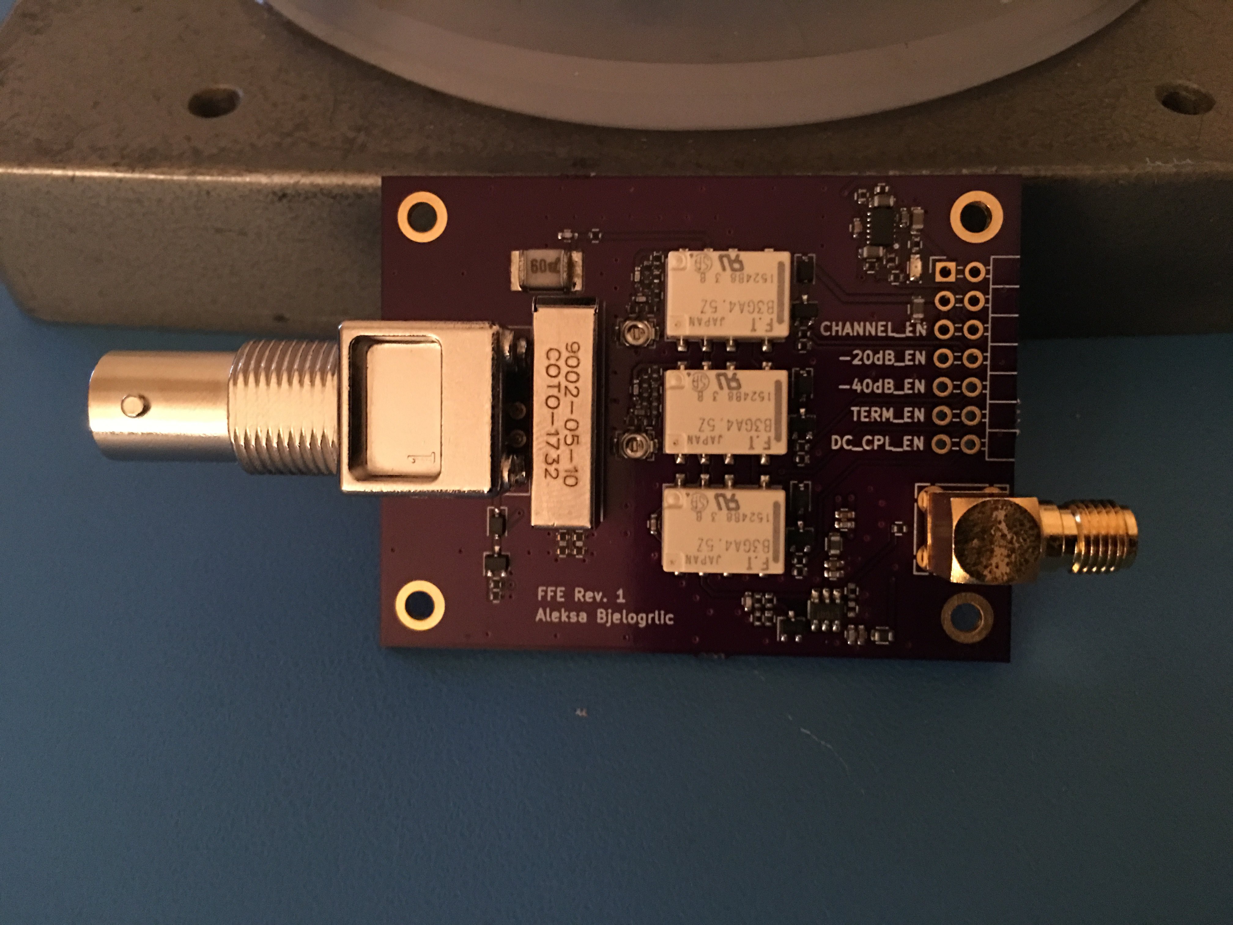
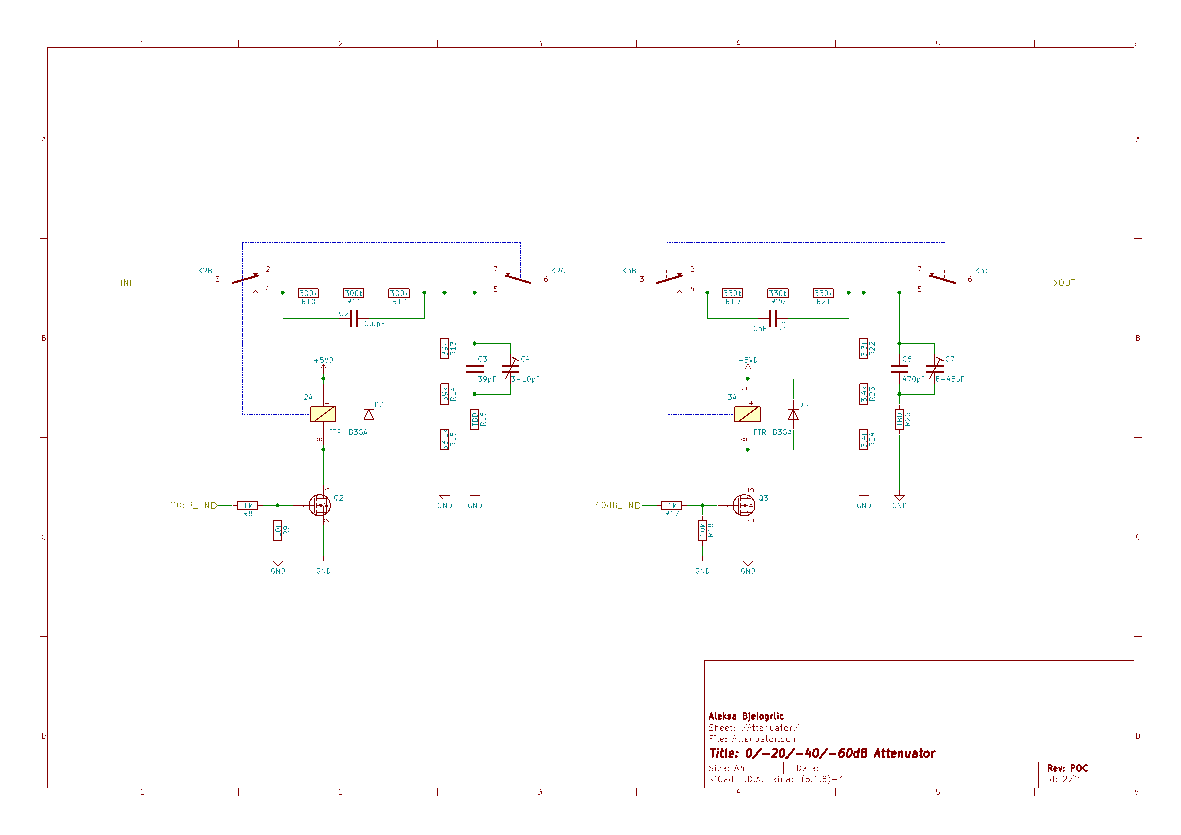
The gas discharge tube (GDT1) provides some degree of input protection, while the reed relay (K1) provides the switchable 50 ohm termination. C1 and C9, alongside R28-30, provide the required 1MΩ//15pF input impedance when the attenuators are off. The attenuators are compensated voltage dividers designed to present the same impedance (1MΩ//5pF) as C9//R28-30 when switched on or off by the relays. R7 should really have been in front of D5 and R31 removed in order to provide protection to the opamp input without adding series resistance that risks lowering the bandwidth of the system. The K4 relay provides selectable AC or DC coupling by switching C8 in or out of the circuit. The opamp circuit is an amplifier in a non-inverting configuration, with a 50Ω output impedance, set by R34, and a SMA output for direct connection to equipment for testing. The LM27762 was used to generate clean positive and negative rails (an integrated LDO cleans up the noisy output from the charge pump used to invert the input). Finally, a right angle 2x7 header connects the various enable signals to the upcoming PGA board, while allowing manual tests to be conducted with jumpers.
![]()
![]()
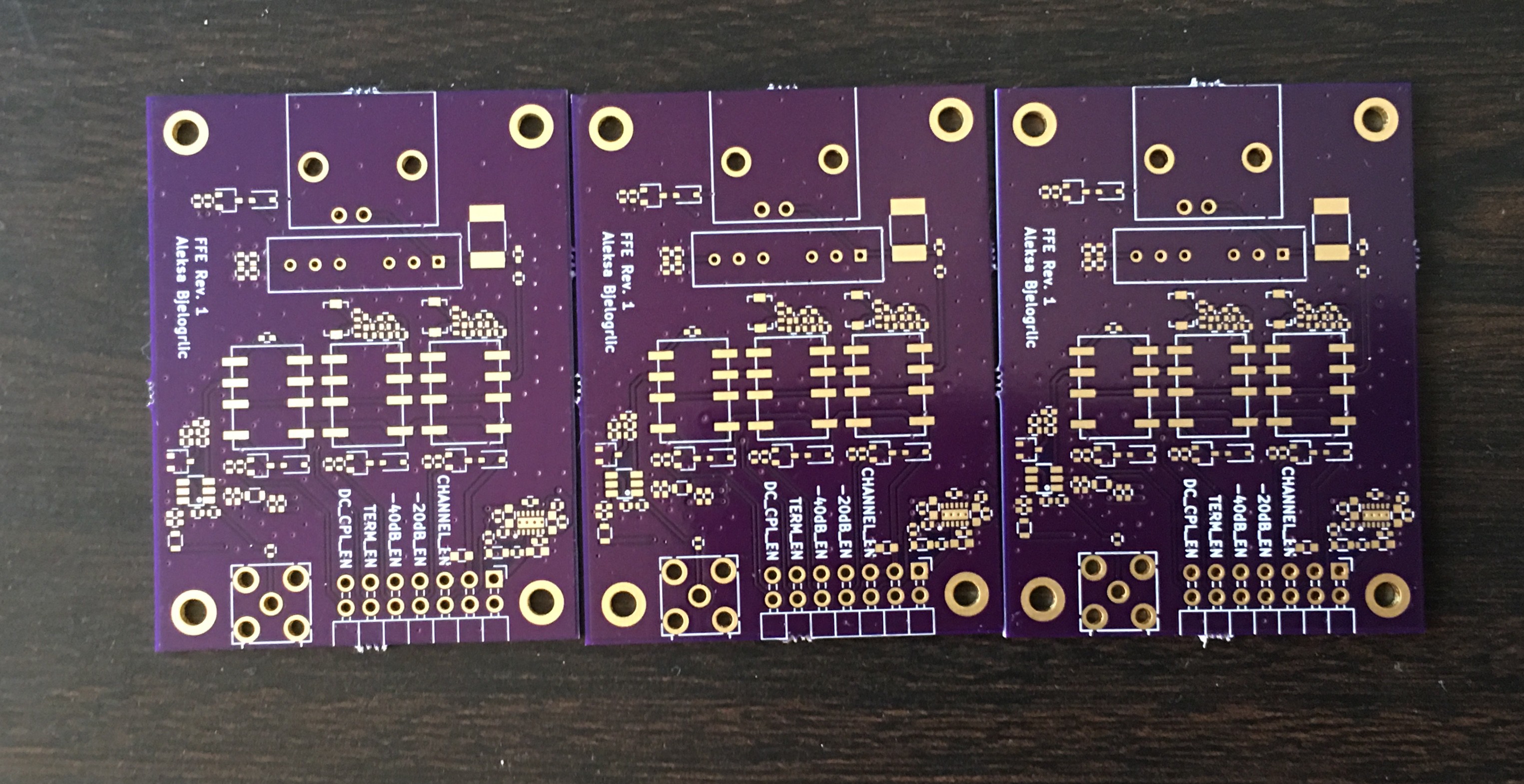
From perfect purple PCBs to potentially performant prototype - thanks to OSHpark's four layer service, aluminium stencil from OSHstencils, and an afternoon under the microscope! At the time this photo was taken, I either ordered the wrong headers or forgot to order them entirely, but who manages to make only one order for a board anyway? In my next post, I'll discuss this revision's test results, problems encountered, and a hasty band-aid solution that proved I should always get a good night's sleep before sending out a new board!
Thanks for giving this post a read, and feel free to write a comment if anything was unclear or explained poorly, so I can edit and improve the post to make things clearer!
-
Intro
05/30/2021 at 17:19 • 0 commentsThe origins of this project lie in [bunnie & xobs'] excellent Novena project, which came about around the time I first became interested in hardware. The Novena had an FPGA co-processor tightly coupled to its CPU, which was used alongside a high speed ADC and a front-end (housed INSIDE a probe!) to make an oscilloscope module. This, alongside much aspirational viewing of [Dave Jones'] oscilloscope reviews and tear-downs, got me thinking about designing an oscilloscope myself.
Software Defined?
After bouncing some ideas off of my friends at university, I became convinced it would be possible to transfer every sample from the ADC to the user's computer in real time, with all the triggering and processing being done by the CPU. This would offer huge advantages compared to regular benchtop scopes! Your sample memory would only be limited by the amount of RAM on your computer, as opposed to the piddly 24 Mpts on scopes such as the ever-popular Rigol ds1054z. Waveform update rate could exceed the 1 million waveforms per second offered by Keysight's InfiniiVision series since processing is done on a modern multi-core CPU, unrestrained by BOM cost limitations on FPGAs or by the fixed nature of ASICs. Speaking of BOM cost, by not having to pay for any real processing, memory, display or power supply, this design can be made competitively to other low cost scopes. This savings also allows for a more capable front end, allowing you to get the most of the 1Gs/s ADC by offering 100 MHZ bandwidth on four channels, 200 MHz on two channels, and 350 MHz on a single channel.
Block Diagram
Here was my initial sketch of the design in March 2018. Sorry for the poor resolution, I knew the photo existed somewhere, but could only find a thumbnail file!
![]()
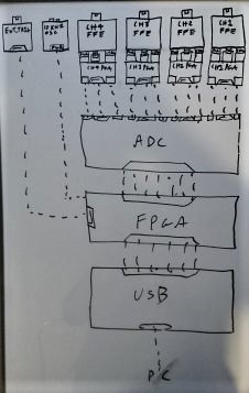
You can see the influence from the Novena oscilloscope module in planning to use all those SATA connectors and in the choice of PGA. The idea was to make the whole system modular, so that each part of the scope could be tested individually. From left to right at the top, we have an external trigger, 10KHz probe compensation, and a module for each channel labeled FFE, for Front of Front End. These modules would hold the input buffer for the next module down the line, the Programmable Gain Amplifier (PGA). This would drive the ADC inputs, and the ADC would connect to the FPGA. The FPGA would handle the external trigger, probe compensation, and convert the ADC's output into something the USB interface could understand. Finally, the USB interface would send all the data to the user's computer.
At the time, there were USB 3 Gen 1 (5 Gbps) interface ICs available and the faster Gen 2 ICs were promised to be in the works. So a Gen 1 chip was chosen with the plan to migrate to Gen 2 when the ICs became available. The parts linked were the ones chosen at the time, so stay tuned for the individual posts for each of the blocks above! Except the external trigger, I dropped that almost right after making this block diagram.
 To use the input signal from the FFE with this chip, it had to be level shifted from +/-2.5V to 0-5V to fit within the PGA's positive voltage range. This was done by a pair of resistors (at the cost of a 2x attenuation!). DC offset control was accomplished by feeding a DAC output into one end of the PGA. This board also forced me to standardize on a connector series to use for the rest of the prototype. I ended up going with the

 I used the same
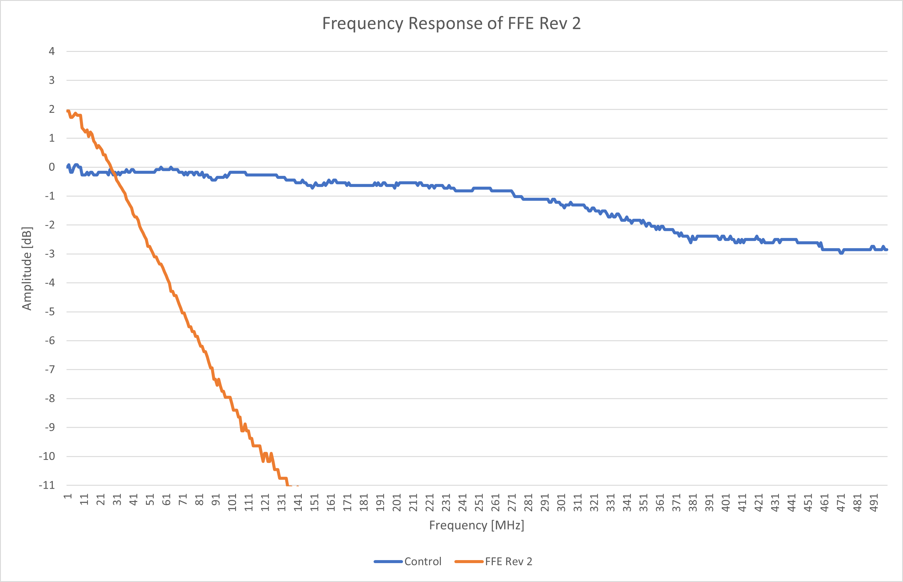
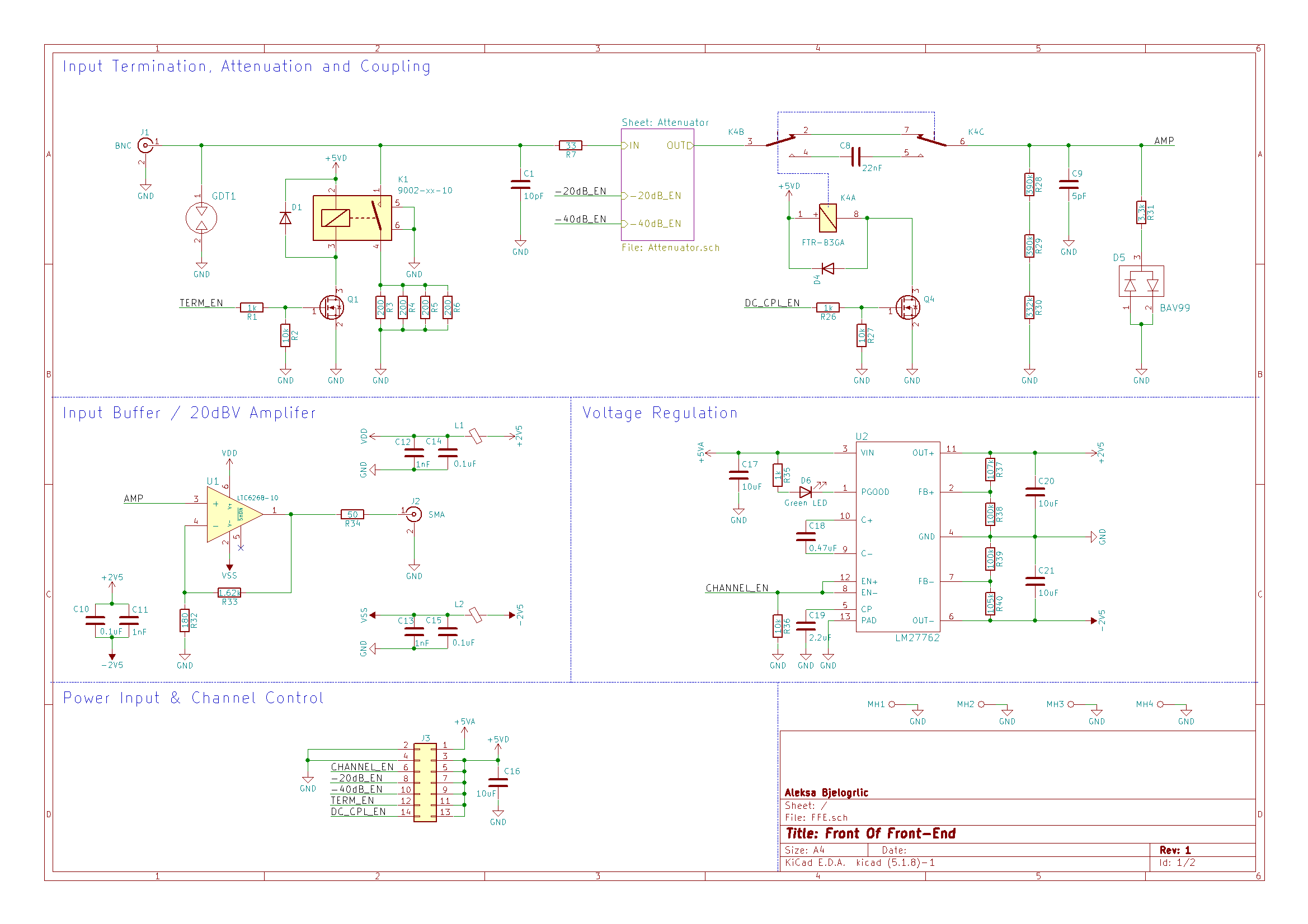 The gas discharge tube (GDT1) provides some degree of input protection, while the reed relay (K1) provides the switchable 50 ohm termination. C1 and C9, alongside R28-30, provide the required 1MΩ//15pF input impedance when the attenuators are off. The attenuators are