Aleksa
-
Crowd Supply Launch
09/20/2024 at 17:10 • 0 commentsSix years ago I had the idea to make an open source oscilloscope, a scope I wish I had when I started playing around with electronics. Three years ago it was a working proof of concept that I documented online, hoping I'd find people who were interested in making it happen. I did, and I can't express how grateful I am for it! Through our shared efforts, I'm so proud to announce that ThunderScope is finally ready for your lab bench: https://www.crowdsupply.com/eevengers/thunderscope
-
Peak[ing] Performance - 50 Ohm Mode Bandwidth
08/04/2024 at 19:03 • 0 commentsHad to split this one into 50 Ohm and 1 MOhm Paths so it wouldn't be too long - and it still ended up being half an hour!
-
When Zero Isn't Zero: DC Offsets in Oscilloscopes
07/26/2024 at 20:14 • 0 commentsTurns out the arrows did work last time? Either that or it was the extra jokes I added in. Anyway, this one doesn't have much intentional humor but the real joke is my slow descent into madness told over hours of videos on scope front ends.
-
Low Frequency Path - A Crossover Double-Cross
07/21/2024 at 18:18 • 0 commentsThinking about the poor intern that wrote an arrow detection algorithm for the auto-select thumbnail option. Wonder if the arrow thing actually works? We'll find out!
-
Real Scopes Have (Derating) Curves
07/17/2024 at 00:49 • 0 commentsA clickbait title for a very dry technical video post. I have included one [1] gag for your viewing pleasure.
-
I can't write good, so I'm making videos now
07/14/2024 at 15:03 • 0 commentsI'm starting a series of technical documentation videos that explain every component in the ThunderScope front end - focusing on a different aspect of the circuit every time, groundhog day style. Hope you enjoy it - or at least find it useful for understanding oscilloscopes.
-
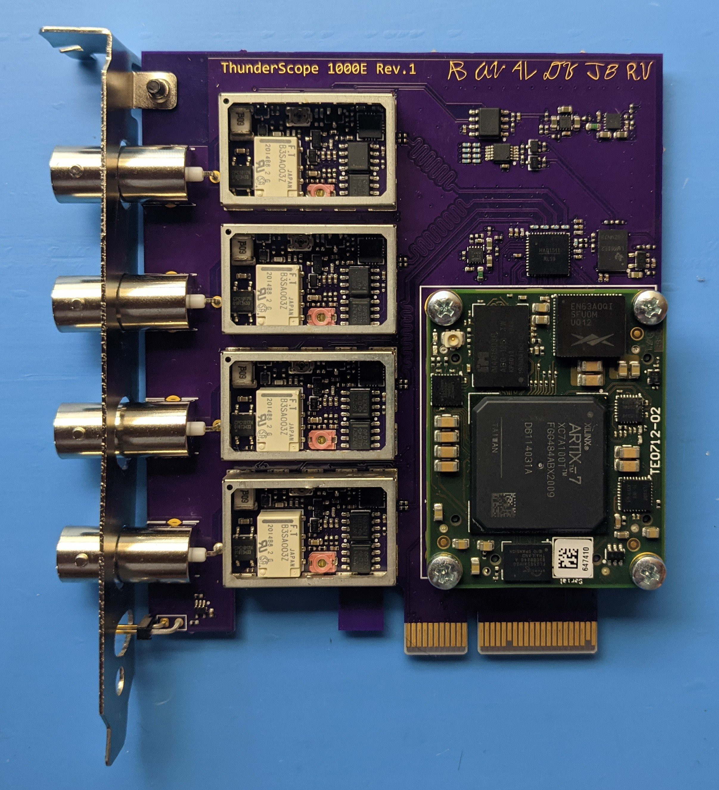
FPGA Module: Extreme Artix Optimization
04/25/2022 at 02:33 • 1 commentIt's been a while since I posted one of these! I've got a few days before another board comes in so I figured I'd post a log before I disappear into my lab once again. Hardware-wise, we left off after the main board was finished. This board required a third-party FPGA module, which had a beefy 100k logic element Artix-7 part as the star of the show, costarring two x16 DDR3 memory chips.
![]()
But wouldn't it look better if it was all purple? The next step was to build my own FPGA module, tailored specifically to this project.
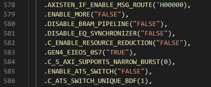
---------- more ----------First, I did a few optimizations to the FPGA design to make it fit into the 35k logic part. Most of these involved digging around in the PCIe core, changing whatever values I could and seeing if it lowered the logic count without affecting performance.
Could it be that easy? Unfortunately not, enabling "resource reduction" only saved a couple hundred LUTs (look-up tables, a finite FPGA resource).
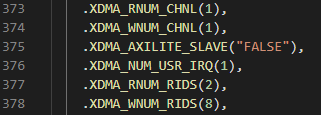
The GUI does not allow you to disable the read DMA channel, so I set it to the minimum number of RIDS I could to try to reduce the logic used by this unused channel. But in the code was an opportunity not just to go to zero RIDs, but to perhaps disable the channel completely! After a very tense compile cycle, it netted a savings of a few thousand LUTs! More importantly, it kept working with the software too (as it never even instantiates the read channel).
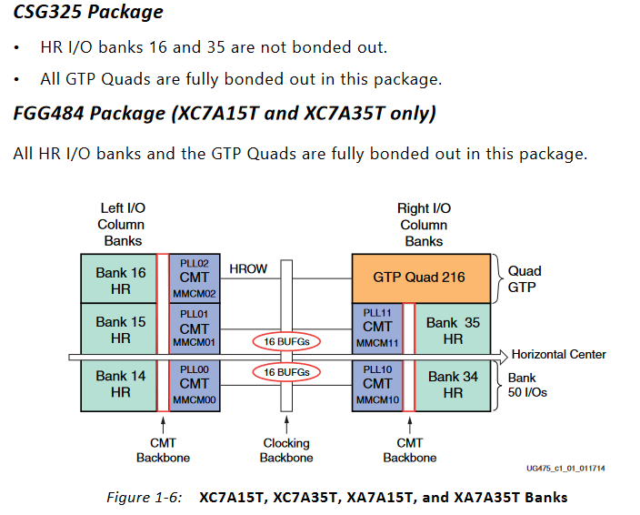
Now that the code fit the smaller (in logic count) part, I decided to use the physically smaller CSG325 package part as well to lower costs even further (the CSG325 is about $10 cheaper through distributors than the FGG484). This came with a few challenges! First, the IO banks for the ADC LVDS lanes (which had to be 2.5V to use internal termination) and the other GPIO (all 3.3V) would have to be merged. I resolved this by using external termination resistors on the LVDS lines to allow the whole bank to be powered by 3.3V.
The next challenge was fitting a x32 wide DDR3L interface on this part. This required two IO banks in the same IO column.
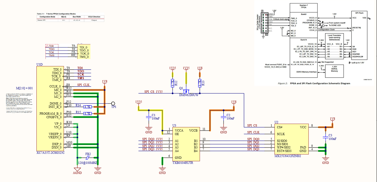
The only two banks that would work were banks 14 and 15, however bank 14 also holds the SPI signals for configuring the part from an external flash memory. There are only five of these signals so it isn't a problem of using too much IO, but again a problem of IO voltage. DDR3L runs at 1.35V and most SPI flash won't run lower than 1.8V, so some sort of level conversion was needed. Luckily enough, someone at Xilinx had thought of this and detailed how to do it in this appnote.
The configuration interface is the one thing you can't reconfigure, got to be careful.
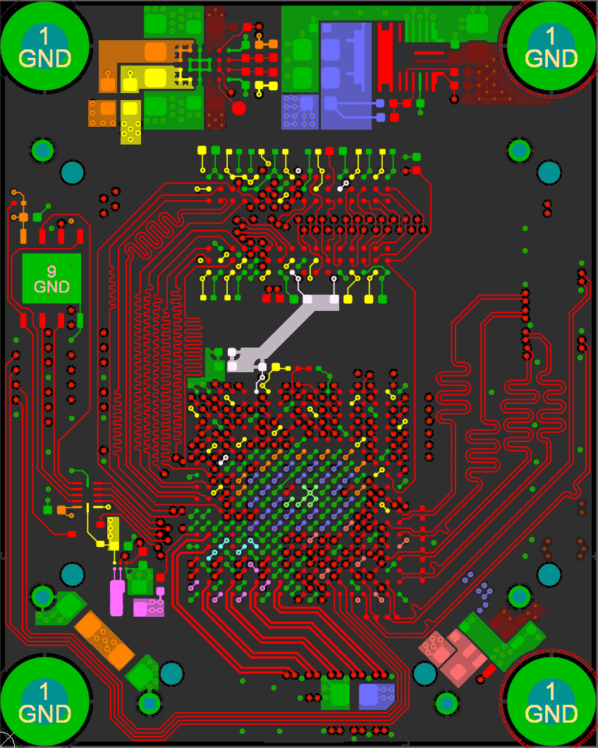
With the schematic sorted out, it was time to layout my first design with a big BGA part and DDR3 memory!
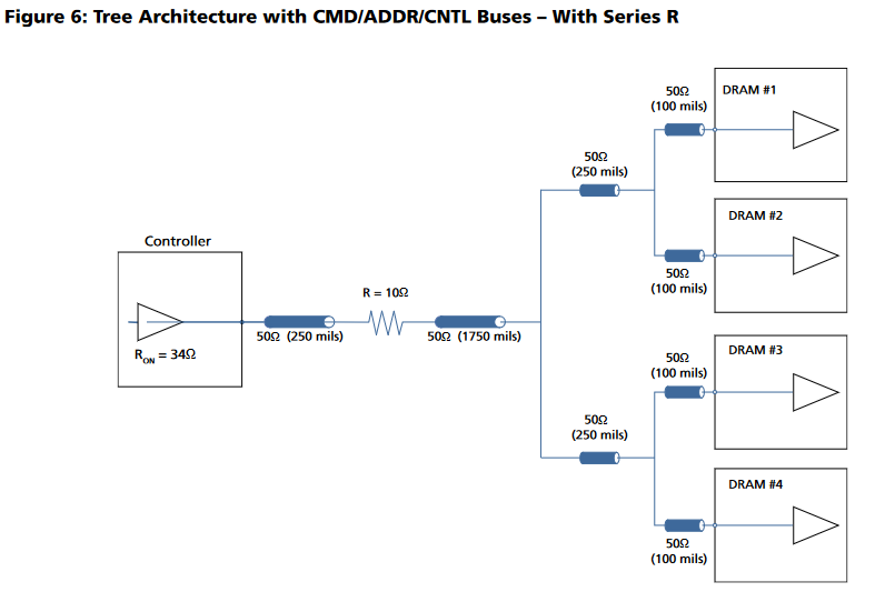
This diagram shows the way I routed the non-data signals (all data signals have on-die termination and don't branch out). Each branch of the tree must have equal lengths as well.
![]()
I accomplished this by placing the two DDR3 chips in the same location, one on the top and one on the bottom. I then length matched each trace on both sides (the branches) to a field of vias and brought all the signals out to the FPGA on another layer.
![]()
Open the above GIF in another window if it's stopped and you'll see the whole layout. The rest of the data signals just needed some length matching, though it was tough to fit all those signals in to each layer!
![https://cdn.discordapp.com/attachments/909600035786878987/941342101545820240/PXL_20220210_043039082.jpg]() After placing *wayyy* too many 0201s, here it is next to the module its replacing!
After placing *wayyy* too many 0201s, here it is next to the module its replacing!![https://cdn.discordapp.com/attachments/909600035786878987/941342102619586590/PXL_20220210_044232292.MP3.jpg]() And finally, the purely purple prototype! Follow this project to catch the next mainboard revision, where we will be integrating Thunderbolt in a supremely janky way!
And finally, the purely purple prototype! Follow this project to catch the next mainboard revision, where we will be integrating Thunderbolt in a supremely janky way!
Thanks for giving this post a read, and feel free to write a comment if anything was unclear or explained poorly, so I can edit and improve the post to make things clearer!
-
Demo Video!
11/07/2021 at 00:01 • 0 commentsGithub Repo:
https://github.com/EEVengers/ThunderS...Discord Server:
https://discord.gg/pds7k3WrpKCrowd Supply:
https://www.crowdsupply.com/eevengers/thunderscope -
Software Part 2: Electron, Redux and React
10/30/2021 at 19:12 • 1 commentDespite the name of this project log, we aren't talking about chemistry! Instead, I welcome back my friend Andrew, who I now owe a couple pounds of chicken wings for recounting the war stories behind the software of this project!
We’re coming off the tail end of a lot of hardware, and some software sprinkled in as of the earlier post. Well my friends, this is it, we’re walking down from the top of Mount Doom, hopefully to the sound of cheering crowds as we wrap up this tale. Let ye who care not for the struggles of the software part of “software defined oscilloscope” exit the room now. No, seriously, this is your easy out. I’m not watching. Go on. Still here? Okay.
Let’s get right to the most unceremonious point, since I’m sure this alone is plenty to cause us to be branded Servants of Sauron. The desktop application, and the GUI, is an Electron app. I know, I know, but hear me out. For context, Electron is the framework and set of tools that runs some of the most commonly used apps on your computer. Things like Spotify and Slack run on Electron. It is very commonly used and often gets a bad rep because of various things like performance, security, and the apps just not feeling like good citizens of their respective platforms.
All of these things can be true. Electron is effectively a Chrome window, running a website, with some native OS integrations for Windows, macOS and Linux in general. It also provides a way for a web app to have deeper integrations with some core OS functions we alluded to earlier, such as the unix sockets/windows named pipes system. Chrome is famously known for not being light on memory, this much is true, but it has gotten significantly better over the last few years and continues to be so. Much the same can be said for security, between Chrome improvements that get upstreamed to Chromium and Electron specific hardening, poor security in an electron app is now often just developer oversight. The most pertinent point is the good citizenry of the app on its platform. Famously, people on Mac expect such an app to behave a certain way. Windows is much the same, though the visual design language is not as clearly policed, many of the behaviours are. Linux is actually the easiest since clear definitions don’t really exist, this has led to, funny enough, the Linux community being some of the largest acceptors of Electron apps. After all, they get apps they may otherwise not get at all.
As much as I would love to write a book containing my thoughts on Electron, I am afraid that’s not what this blog calls for. So, in quick summary, why Electron for us, a high speed, performance sensitive application? I will note this, none on the team were web developers prior to starting. It is very often the case that when web developers or designers switch over to application development, they will use Electron in order to leverage their already existing skills. This is good, mind you, but this was not the case for us. We needed an easy way to create a cross platform application that could meet our requirements. In trying to find the best solution, I discovered two facts. Fact the first, many other high speed applications are beginning to leverage Electron. Fact the second, finding out that integration with native code on the Electron side is not nearly as prohibitive as I initially thought. So, twas on a faithful Noon when I suggested to our usual writer, Aleksa, that we should give Electron a whirl. I got laughed at. Then the comically necessary “Oh wait no you’re serious”. I got to work, making us a template to start from and proving the concept. That’s how we ended up here.
---------- more ----------![]()
Last we left off, we were shooting data into the blackbox that was our GUI. Continuing from there, our data goes into something called a Context Isolation pipeline. Without going too deep into it, Context Isolation is an Electron feature that runs your own Electron scripts and APIs in a separate context than the website running within the app. This is important for security, as a website could potentially inject code using these very powerful APIs.
The data goes through internal processing, where the packets are broken down into their actual data in order to be analyzed and displayed by the app. From the opposite direction, this is also where packets including scope commands would be formed before being sent. From there, we go off into React. While Electron is our app framework, we chose to use React for our UI needs. Put simply, it is very common with lots of available resources. Since the data is now in a format TypeScript can understand, it is passed onto the graphing library.
Due to time constraints, we chose to not roll our own graphing library. We knew that in time, we would have to, but for now an open source React based solution would have to suffice. This is our second reason for picking React, the litany of options. We chose react-vis, made and maintained by the fine folks over at Uber. I should note that this whole pipeline needs to be ridiculously fast. As such, we do the bare minimum of processing in Electron, as most of it would have been done in C++ already, including measurements. By the time the data arrives in the app, we fast track it to the graph. As part of this process, labels in the app get updated, such as the measurements of various channels like mentioned before.
![]()
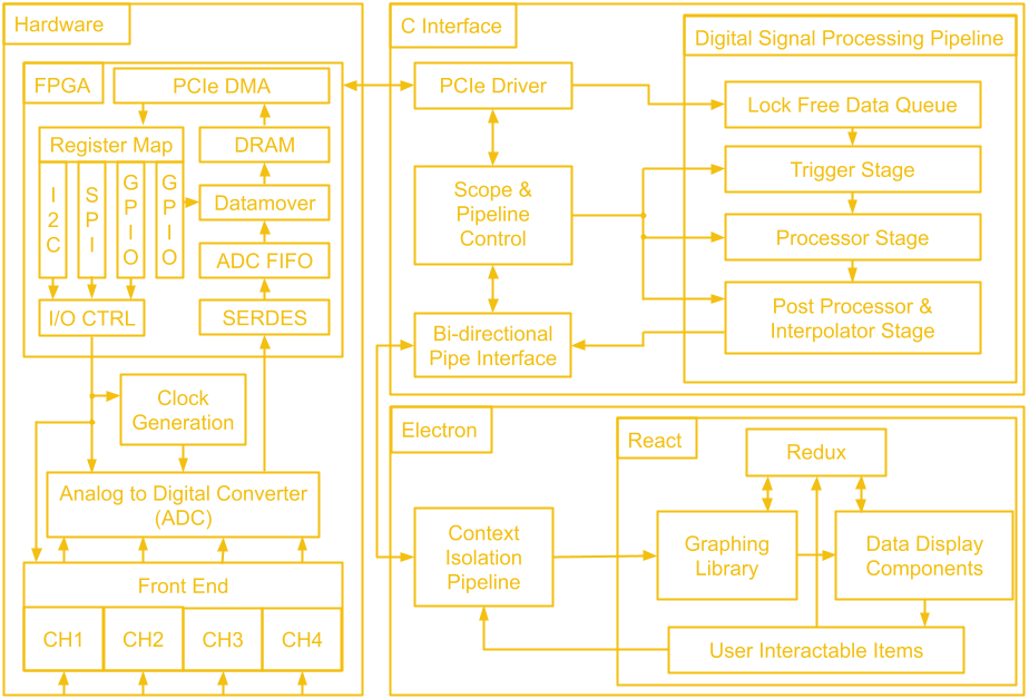
The right hand side column is what we call the “Data Display Components” on the block diagram. This encompasses both read-only labels, as well as the buttons and selectors, which we’ve so aptly called “User Interactable Components”. A user can change the type of math being done between channels, such as addition and subtraction using these. The user can also enable or disable channels here. Certain interactions, such as channel switching, trigger a scope control message to be sent out, following our packet pipeline the other way, as we have often talked about. The instruction is encoded, sent along in a packet, and the C++ uses the driver to trigger the correct function inside the FPGA, and the wonderful loop continues still. This forms the conclusion of the basis of our data loop and how it functions. While the feature set can yet be expanded on, and most of the remaining work is indeed application side, the solid foundation provides a healthy landscape for continued work.
![]()
I want to take just a moment to discuss how technical challenges evolve over time, and in this, address the one block I have ignored on our block diagram. As you can see from our prototype, the design has changed, but not massively. We’re engineers, making a tool for engineers. We recognized early on that we were not designers, and we knew that making the nicest to use piece of software would take a lot more time than we had available to us. As such, we strived to create a solid base, almost a good wireframe, that could be iterated upon. I hope this explains why some of the usual creature comforts one would expect to happen are not yet present. We wanted to ensure in anything we did, we didn’t accrue tech debt or create future work for ourselves. At least not wittingly. This careful approach would allow us to build up in the future without having to tear down massively before (we did consider using some big open source react elements library to make things look nicer on the short term, but we thought that disingenuous).
As for that last block, Redux. Anyone familiar with React is likely to be familiar with Redux as well. We’re all familiar with state machines in the most traditional sense, it helps keep a system working as it should with all components being on the same page effectively. Redux is not a state machine. It does not enforce explicitly a state within a graphically expressible state diagram. Instead, it uses triggers to send out commands using actions based on requirements defined by the designer. This sounds like I’m saying “It’s not a state machine, it’s a state machine”. I basically am saying that, because the logic for switching states in Redux looks an awful lot like any state machine (in web land, XState is a popular tool). The key difference however, is that Redux does not prevent variables and status linked to states, from being changed by anything other than Redux. It is possible for you to code for impossible states and to end up in unrecoverable positions.
We all know that state based management is the best way to control a relatively complex system. We tried to stay away from it in our own app, but eventually we found out we were creating unnecessary complexity to avoid, slightly less complex complexity (something about unwitting tech debt anyone?). Yet, while Redux solved many of our issues, it also caused a decent amount of extra work based on the lack of safe guards provided. This perhaps serves as a cautionary tale and a good reminder that control systems itself continues to be perhaps the most crucial of all disciplines.
Thanks again to Andrew for the excellent write-up of the software! And with this post, you are pretty much caught up on the development of this project. With all the documentation done, check out all the source goodness at the git repo for this project, and stay tuned for the demo video coming up in the next post!
Thanks for giving this post a read, and feel free to write a comment if anything was unclear or explained poorly, so I can edit and improve the post to make things clearer!
-
Software Part 1: HDL, Drivers and Processing
10/21/2021 at 01:07 • 0 commentsWe've gone through a lot of hardware over these last 14 project logs! Before we leave the hardware hobbit hole to venture to software mount doom, let's take a look at the map of middle earth that is the block diagram of the whole system.
![]()
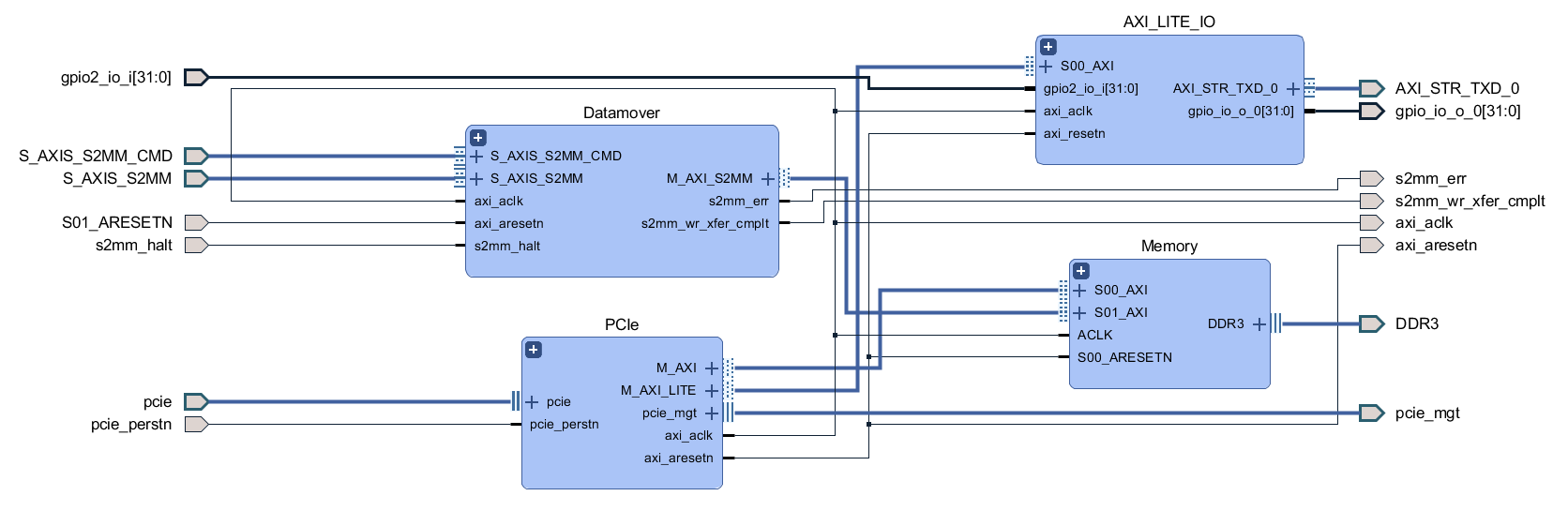
The first block we will tackle is the FPGA. The general structure is quite similar to the last design, there is ADC data coming in which gets de-serialized by the SERDES and placed into a FIFO, as well as scope control commands which are sent from the user's PC to be converted to SPI and I2C traffic. Since we don't have external USB ICs doing the work of connecting to the user's PC, this next part of the FPGA design is a little different.
There is still a low speed and a high speed path, but instead of coming from two separate ICs, both are handled by the PCIe IP. The low speed path uses the AXI Lite interface, which goes to the AXI_LITE_IO block to either fill a FIFO which supplies the serial interface block or to control GPIO which read from the other FPGA blocks or write values to the rest of the board. On the high speed path, the datamover takes sample data out of the ADC FIFO and writes it to the DDR3 memory through an AXI4 interface and the PCIe IP uses another AXI4 interface to read the sample data from the DDR3 memory. The reads and writes to the DDR3 memory from the AXI4 interfaces are manged by the memory interface generator. The memory here serves as a circular buffer, with the datamover always writing to it, and the PCIe IP always reading from it. Collision prevention is done in software on the PC, using GPIO data from the low speed path to determine if it is safe to initiate a read.
---------- more ----------With the deadline of the Hackaday prize fast approaching, I have called my friend Andrew out of retirement to write the rest of the software project logs. He worked on the software far more than I did, so he can give you a better overview of it! Plus he's not a chronically slow writer like I am, two project logs a month isn't too bad right?!
Next, we will question our life decisions as we begin ascending up the slope to Sauron’s domain and talk about the C interface implementation. The data is moved over PCIe by the PCIe IP's driver, also provided by Xilinx. PCIe is notoriously quite difficult to properly implement on the software side (quite the opposite from its hardware requirements) and while we considered writing a custom driver, we found that the off the shelf driver fit our requirements splendidly. This allowed our efforts to be focused elsewhere.
The driver itself passes the data to two separate sections of our C program. The first is the scope control mechanism. This is part of our bi-directional control system that allows the scope to tell the GUI the current state of the hardware (more on that in a later post), while allowing the user to change said state. Certain settings, such as voltage ranges, are not only software display options, but actually result in hardware changes in order to enable more granular reading of data.
The other data that the driver handles is, of course, the readings of the scope itself. This data takes a slightly different path as it requires some processing that would traditionally be done on the on board processor on a scope. The data first enters a queue, a circular buffer that gets processed each time it receives enough data. Specifically, this circular buffer is being analyzed for a possible trigger event, such as a falling/rising edge, as called in traditional scopes. This is such that the software knows when to lock in the data for presentation to the user.
Once a trigger event is discovered however, it then passes to the post processing and the interpolation stage. We process the data internally to make sure it conforms to the voltage and time scales expected according to the scope’s current state, and interpolate missing data based on sinx/x interpolation, the standard in oscilloscope design. You might notice that about half of the processing block is not directly related to hardware itself, but is actually present solely to ensure that the data can be accurately displayed to the user in the GUI. This is one of the challenges of such an implementation, where different components that are not self contained within the scope hardware have to sync up and communicate seamlessly.
Once the data has been processed, it is passed to the bi-directional pipe interface, where we once again meet up with our scope state information, ready to be passed onto our GUI (once again, more on that in a future post). In order to understand the choices we’ve made however, it is important that we explain exactly what our data pipeline is. On Linux we use UNIX Sockets, a quite simple, packet based IPC protocol that will be familiar to anyone that has had to make two programs talk before. We initially used a single bi-directional pipe. This brought about some challenges but with some timing sync logic, it worked out.
Then we looked at implementing the Windows logic. On Windows, the equivalent is something called Named Pipes. These do not really support bi-directional data transfers. The more suggested path, however, is just two parallel one way pipes. Upon testing we didn’t see any performance degradation on the Electron side. Turns out web browsers are quite good at handling packets, who knew? We also changed the Linux implementation to be the same, just to be able to reuse as much code as possible. The other interesting fact we discovered is that, in trying to keep the packets lean, we ended up with quite poor performance on the GUI side. It turns out that on Windows, there’s a upper limit on the top speed of packet delivery, a sort of “next bus” problem.
This does not change regardless of how much data you pack into one packet, up to a maximum limit. As such, the pipe towards the GUI packs enough data such that if we fill every available “bus”, we achieve 60fps on the display. The GUI app reads the header of the packet to figure out the beginning and end of actual data versus state updates and separates it as such for processing. On the receiving side, things are very similar. In order to ensure the system stays synced, the GUI also sends overloaded packets to the C program, to keep the side consistent, even though scope commands don’t technically call for this level of data density. Similar to the GUI side, the C program reads the header to know which commands were sent, compares them to a known look up table converting our internal identifier and value to a known “state”, and sends that state down the driver and to the FPGA to work its magic! And that’s all folks. Tune in next time for a deep dive into the Electron app and the GUI.
Thanks for giving this post a read, and feel free to write a comment if anything was unclear or explained poorly, so I can edit and improve the post to make things clearer!
 After placing *wayyy* too many 0201s, here it is next to the module its replacing!
 And finally, the purely purple prototype! Follow this project to catch the next mainboard revision, where we will be integrating Thunderbolt in a supremely janky way!