-
Switched Front Panel CPU Design
07/14/2021 at 12:00 • 0 commentsSwitched out the IOP16 to use the cpu_001 from the Design a CPU. This CPU is designed from scratch and is functionally identical to the IOP16 CPU. The Design a CPU was designed from scratch and adds some extra instructions. There is a video series on YouTube that has the design details of the cpu_001.
-
New Front Panel Demo
07/07/2021 at 19:51 • 0 commentsThe new Front Panel has arrived. It is identical in function to the previous card but uses entirely through hole parts. Here's a little demo showing loopback to the LEDS when a pushbutton is pressed.
-
Sped up CPU to 12.5 MIPs
07/06/2021 at 01:06 • 0 commentsSped up the CPU from 6.25 MIPS to 12.5 MIPS.
Moved the IOP16 CPU into its own GitHub repo.
-
Designed Thru-Hole Front Panel
06/20/2021 at 01:01 • 0 commentsThe current front panel design has some fine pitch parts which make it harder for some to assemble.
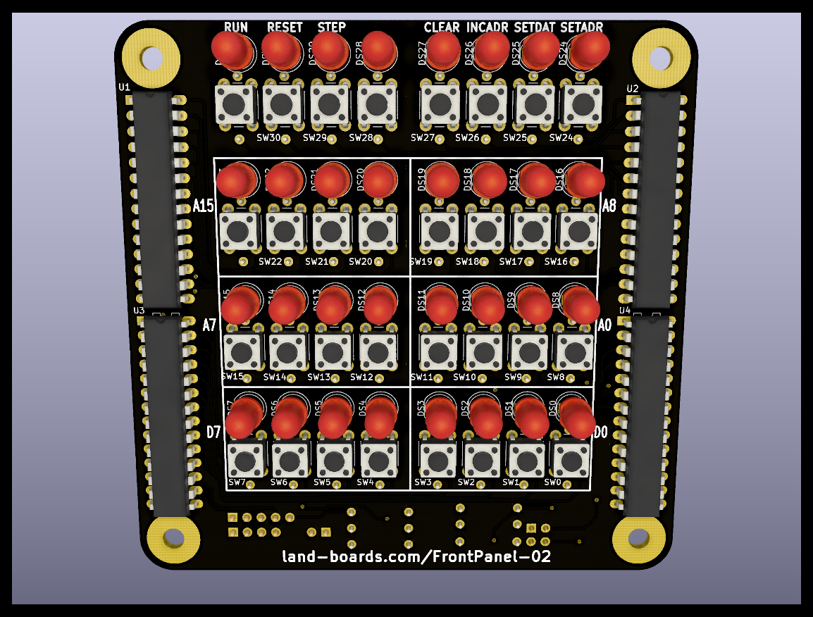
Designed a thru-hole version. It's a bit tight but definitely doable. Will take about a month to order/build/test. After that I will put it up for sale on Tindie. Here's a view of the board and control button legends.
![]()
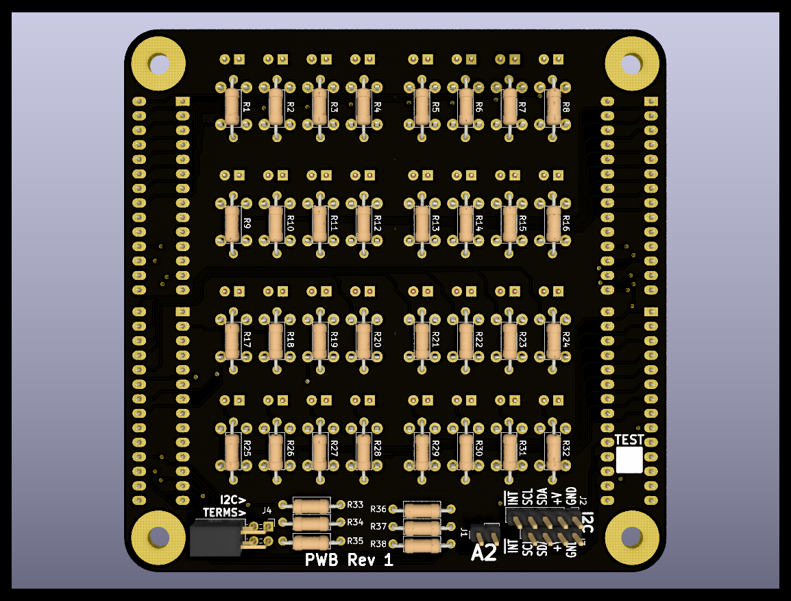
This is the rear side view. The resistors get installed on rear side. The I2C daisy chain, I2C base address and IC termination headers are on the rear side of the card. The I2C headers should be right angle headers to facilitate a lower profile/installation for connection to the FPGA card (mounted below when used with compatible Land Boards cards (like the RETRO-EP4CE15 card).
![]()
-
Front Panel with 6800 CPU
06/20/2021 at 00:43 • 0 commentsGot the Front panel working with a MC6800 FPGA CPU. FPGA Build is here. Same button/LED arrangement.
- RUN/Halt Pushbutton - Stop CPU and enable Front Panel control of memory.
- SETADR button/LED - Allows an address to be entered.
- SETDAT button/LED - Allows data to be entered to load into SRAM.
- INCADR - If SETDAT is active, writes to SRAM then increments address. If SETDAT is not active examines the next memory location.
![]()
Works great!
-
Added JSR/RTS to IOP16
06/19/2021 at 13:41 • 0 commentsCreated a new IOP16 which adds Jump to Subroutine (JSR) and Return from Subroutine (RTS) opcodes to the IOP16 (in new IOP16B VHDL code). This is a single level only. Implementing nested subroutines would require stack memory and additional resources (another 2 memory blocks). A short LIFO could probably be implemented in logic/registers but isn't worthwhile in this application since a single level is enough.
This allows the in-line I2C functions to be replaced with subroutines and greatly shortens the code length. The code runs slower due to the added burden of the two instructions, but this is not a significant issue since speed it not a particular concern. because the I2C interface runs much slower than the CPU.
This implies the passed parameters need to be placed in specific registers which requires careful control.
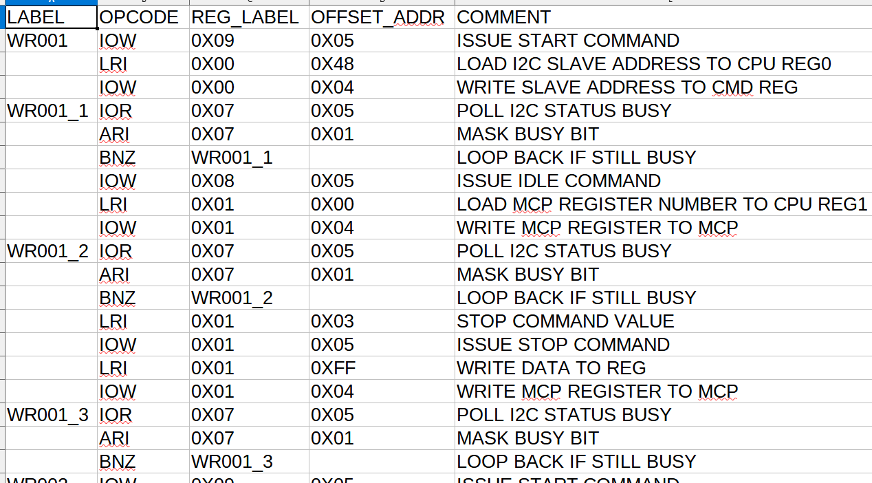
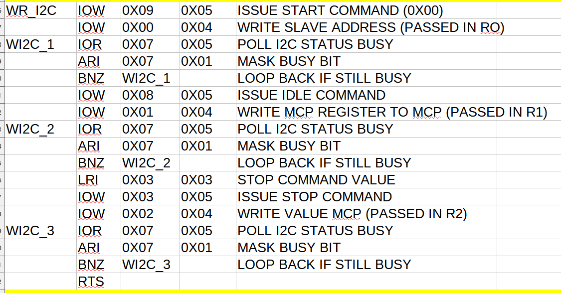
Example of writing a value to an I2C register - before the change.
After the change - the calling code is:
The I2C subroutine code is:
Register Allocations
- R0 = I2C Slave Address
- R1 = I2C Register number
- R2 = Data to write to the I2C I/F / Data that was read from the I2C I/F (return value from the I2C read subroutine)
- R3 = Scratchpad in routines
- R4 = Bogus write value triggers read transfer
- R7 = I2C Busy Status
- R8 - Hardcoded 0x00 value
- R9 = Hardcoded 0x01 value
- RF = Hardcoded 0xFF value
Code Size Reduction
The code size before the change was 975 lines and 243 lines after creating I2C read/I2C write subroutines (JSR and RTS). That's a 75% reduction in code size.
The GitHub branch is here. The code that is run is FP01_LOOP3.
It works!
-
Future Improvements
06/17/2021 at 15:47 • 0 commentsBugs
No known Bugs
Wish List
- Add error handling to I2C (there's an error bit I am ignoring in the status from the I2C controller)
-
Accessing CPU Memory from Front Panel
06/17/2021 at 11:47 • 0 commentsCreated a branch which simulates controlling a CPU memory from the Front Panel. Made the memory an 8KB, Dual Port SRAM in the CPU. Able to read/write the memory.
It works!
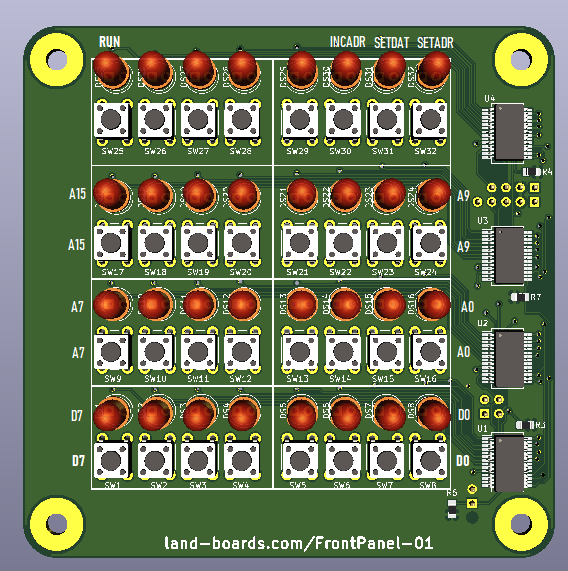
Front Panel controls are:
![]()
The bottom 8 Pushbuttons/LEDS control d0-d7 of the SRAM.
The middle 16 Pushbuttons/LEDs control A0-A15 of the SRAM.
The top 8 pushbuttons control:
- RUN/HALT (toggle pushbutton)
- CPU is running when lit (Run is not used in this case simce there's no CPU being controlled)
- INCADR (debounced pushbutton)
- Stores data then increments address when in SETDAT mode
- Increments address when not in SETDAT mode
- SETDAT (toggle pushbutton)
- When pressed/lit allows Data pushbuttons to change memory data
- SETADR (toggle pushbutton)
- When pressed/lit allows Address pushbuttons to change memory address
- RUN/HALT (toggle pushbutton)
-
Resources With Pushbutton Processing
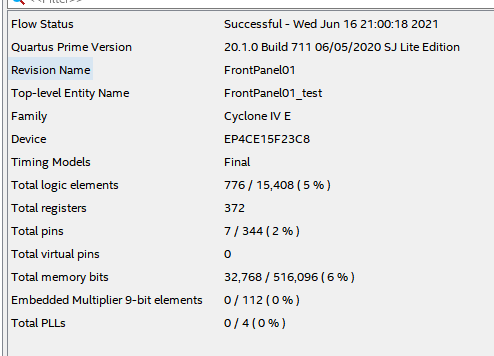
06/17/2021 at 01:05 • 0 commentsThe FPGA size is a bit bigger after pushbutton processing is added.
Still pretty small. The ROM size could be dropped in half since the IOP16 code is under 1K words.
-
Use in FPGA Microprocessor applications
06/16/2021 at 16:00 • 0 commentsThe goal of this project is to use this design in a 8-bit Retro-Computer application. To meet this goal the 32 pushbutton and 32 LEDs need to be mapped to the CPU design.
As an example of this mapping:
- Bottom row 8 LEDs are CPU D0-D7 (toggle pins)
- Next 2 rows up are CPU A0-A15 (toggle pins)
- The top row is control lines/status LEDs (debounced pushbuttons / settable LEDs)
Selection of the function of a particular pushbutton is relatively simple. The bottom 24 bits are toggle buttons. The top 28 buttons should create either single pulses for uses like Reset and toggle pins for uses like Run/Halt. This is done by having the panel VHDL file entity look like:
entity FrontPanel01 is
port
(
    -- Clock and reset
    i_CLOCK_50    : in std_logic := '1';
    i_n_reset    : in std_logic := '1';
    -- 32 LEDs(outs), 32 Pushbuttons (ins)
    i_FPLEDs    : in std_logic_vector(31 downto 0);
    o_PBRaw        : out std_logic_vector(31 downto 0);
    o_PBLatched    : out std_logic_vector(31 downto 0);
    o_PBToggled    : out std_logic_vector(31 downto 0);
    -- The key and LED on the FPGA card
    i_key1        : in std_logic := '1';
    o_UsrLed    : out std_logic := '1';
    -- External I2C connections
    io_I2C_SCL    : inout std_logic;
    io_I2C_SDA    : inout std_logic := '1';
    i_I2C_INTn    : in std_logic := '1'
);
end FrontPanel01;
The relevant signals are:
- o_PBRaw - The pushbuttons as polled (~ ever 1 mS)
- o_PBLatched - Debounced pushbuttons
- o_PBToggled - Toggled pushbuttons
Application Specific Example
For this VHDL code, this means removing the loopback at the top level or more specifically gating with other signals). If the CPU is running, the Data and LEDs should reflect the values on the CPU Data and address lines. If the CPU is halted, the pushbuttons should reflect the address that is being accessed from the front panel.
For an example which is closer to the application, I created a new branch with the bottom 24 lines looped back as toggled pins and the top 8 lines looped back as debounced lines. Also, cleaned up the top VHDL file to move down pushbutton handling one layer lower. This uses the same IOP16 code as the previous log (FP01_LOOP2).
It works!
8 Bit Computer Front Panel
VHDL code for I2C Control of Front Panel with 32 pushbuttons and 32 LEDs
 land-boards.com