Here's the new v0.3 pcb design. Layout has been adjusted to accommodate the change to AH1815-W-7 hall switches.

Since the hall switches needed to be placed on a smaller radius I had to rotate the esp32 board headers by 45°.
Hand soldering the board will be a bit more difficult since everything is a bit more cramped. But overall I'm satisfied with this layout.

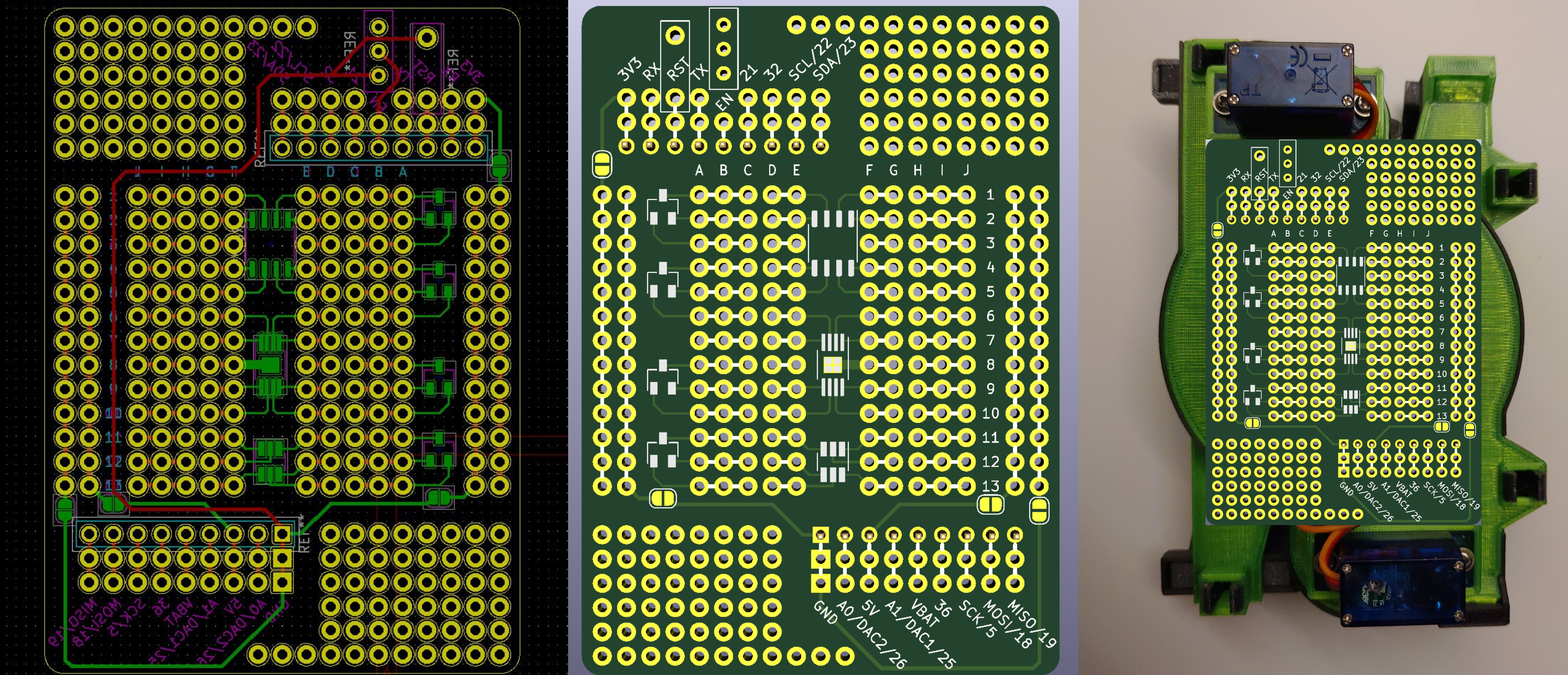
New for this iteration is an expansion shield that fits on top of the controller PCB. It's a through-hole prototyping board that breaks out the unused GPIO from the esp32 board. I also threw in some smd footprints for good measure.
Discussions
Become a Hackaday.io Member
Create an account to leave a comment. Already have an account? Log In.