 deʃhipu
I spent a little bit of time today to design another breakout PCB, this time for the Blackberry 8350 button:
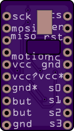
I took the labels from that pinout published it the Arduino forum, but comparing it with the schematic also published there, it seems to be a bit fishy... For example, a pin marked as "gnd" on the pinout is pulled-down to gnd with a 200k
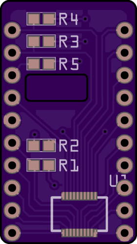
This is also an experiment with physical layout of the board — there is a cutout in the PCB where the flex cable is going through, and a pad where the button will be, so that I can put a drop of solder there, to provide the necessary raised bump for the tact switch on the back.
I'm also not sure whether I should add a voltage regulator and some voltage dividers — the forum post says 2.85V, but I don't actually know if it will work with 3.3V as well. The mouse sensors, which are supposed to be similar, run on 3.3V.
Discussions
Become a Hackaday.io Member
Create an account to leave a comment. Already have an account? Log In.