My 2x SPI FRAM prototype is now up and running and memory mapped in. It now works as normal ram but retains data after power off. This will be used for firmware storage. 1 chip stores upper 8bits the second stores lower 8bits. Because I'm using an FPGA I just add as many SPI interfaces as I need so both chips run in parallel.
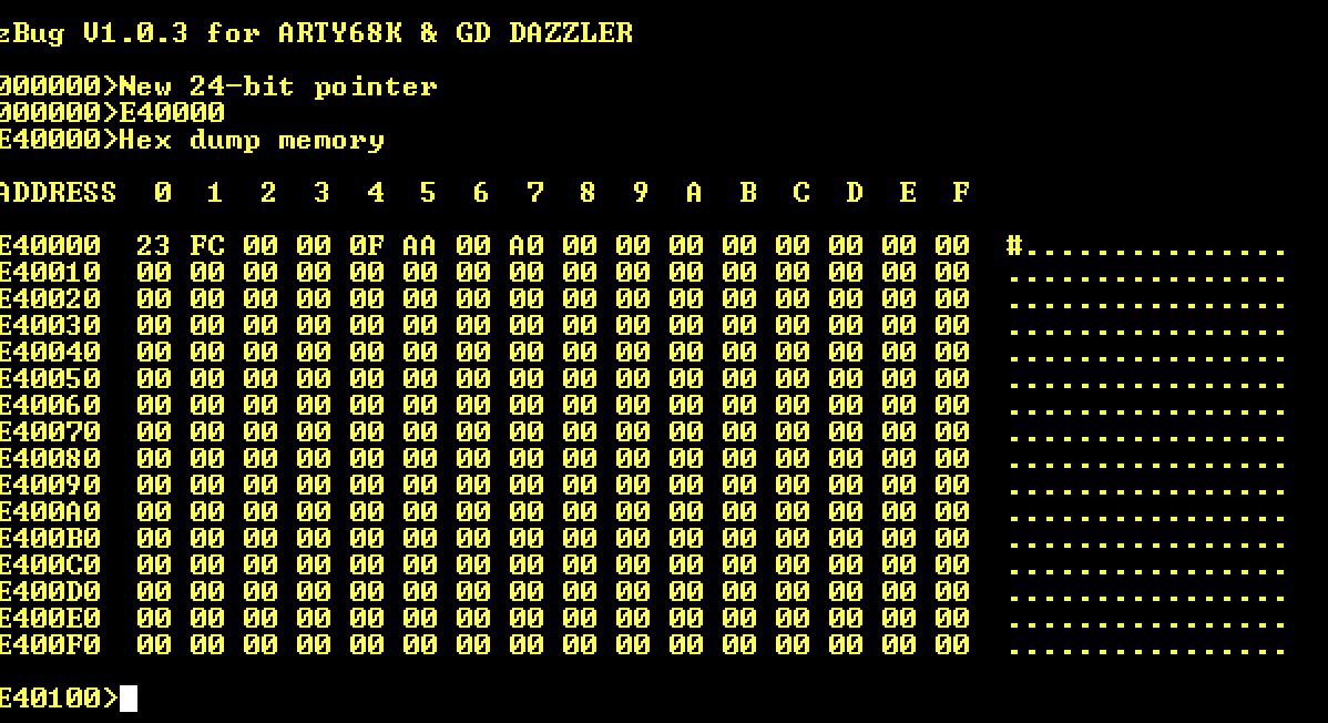
Hex dump of my test s-rec program after being loaded into FRAM.

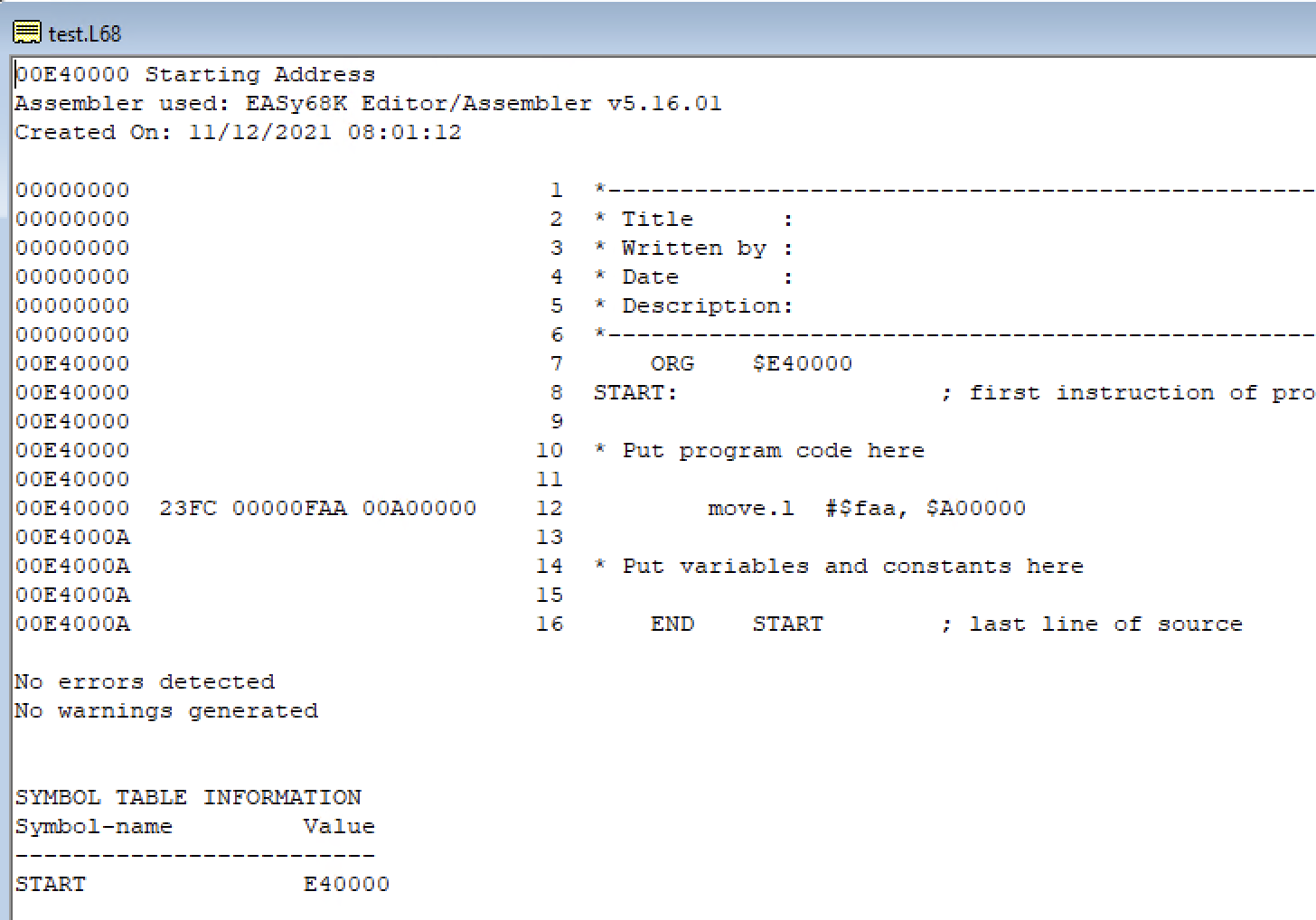
The actual code - FRAM is mapped to E40000-E80000:

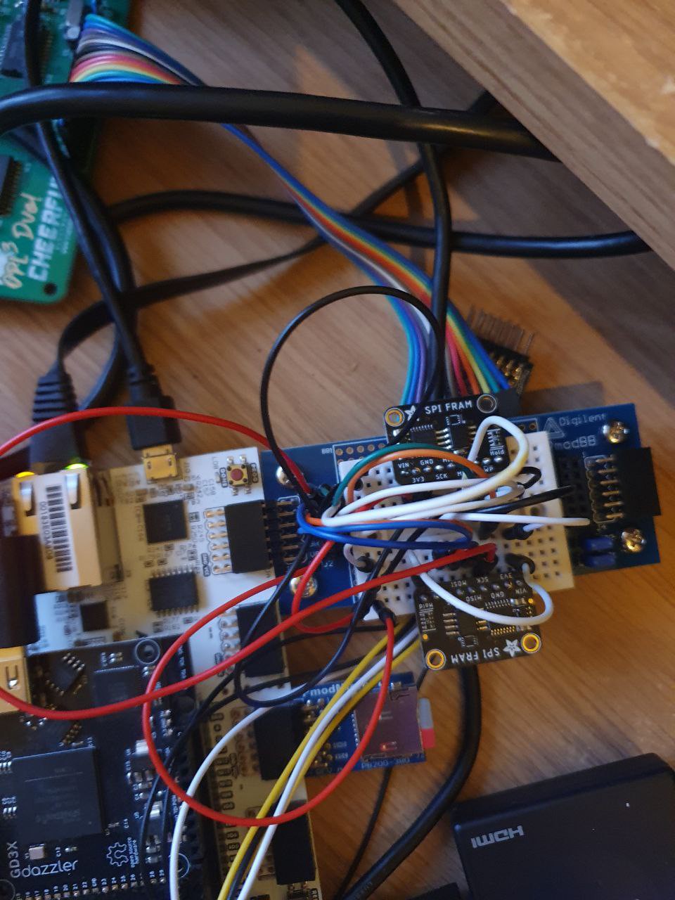
The dual FRAM pmod board prototype.

 Matthew Pearce
Discussions
Become a Hackaday.io Member
Create an account to leave a comment. Already have an account? Log In.