 Matthew Pearce
Despite me saying that was it for hardware, noticed I was getting instability sometimes just because the DDR was just soooo slowwwww. So started investigating caching. Luckily because I use the AXI protocol for my DDR accesses, xilinx already provides an IP block for caching. So it was a fairly simple change to modify my retro axi code to include a call to a cache block as an intermediate.
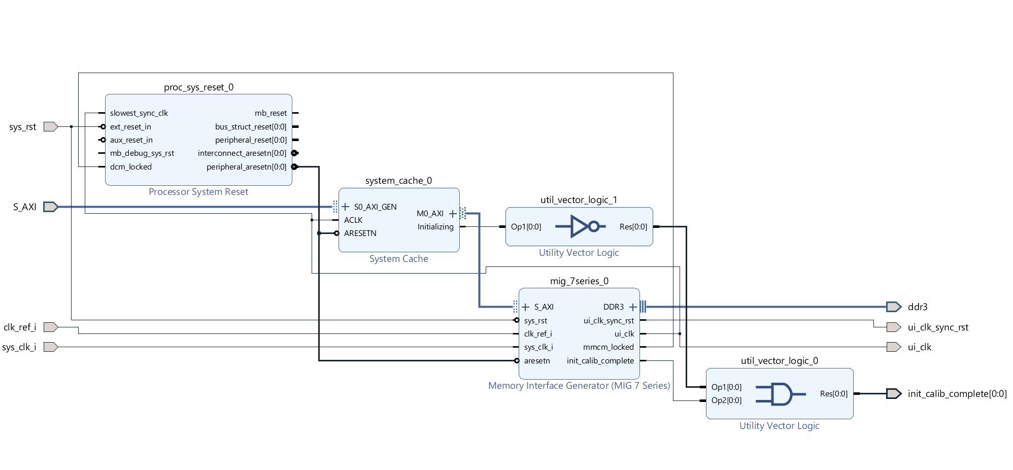
In the project the code looks like this - so as you can see it has a traditional look to the memory interface (aside from the external DDR links). The DDR3 requires a 166 & 200 mhz clock to work correctly. This gives a speed of 83mhz (166/2), which isn't too far off the main system speed and isn't a problem with the cache in-between. In the block diagram below, the S_AXI input comes from my retro-axi master code, into the cache which then handles the traffic to/from the MIG and DDR.
memory:  main_memory_control
    port map(
    sys_clock => cpu_clock,
    sys_resetn => resetn and clk_locked,
    clock166 => clk166,
    clock200 => clk200,
    -- cpu interface (Fast memory)
    address(27) => '0',  -- // Address bus (Upper part not used)
    address(26 downto 4) => cpuAddress(23 downto 1), --ignore last digit. always 0
    address(3 downto 0) => "0000",
    i_cen =>  cpuCS or boot_rom, --     chip select
    i_valid_p => mem_i_valid_p, -- valid input active high
    wr_byte_mask(1) => not cpuUpper, -- upper byte from cpu
    wr_byte_mask(0) => not cpuLower, -- lower byte from cpu
    i_wren => cpuWriteEn, --      Write enable
    wr_data => cpuDataOut, --      Data to write
    rd_data => memDataOut, --     Data to read
    o_valid_p => mem_ack ,--   read ready (link to dtack)
    wr_ack_p => mem_wr_ack, -- write complete (link to dtack)
      o_ready_p => open, -- idle (not used)
    -- DDR3 Inouts
      ddr3_sdram_addr   => ddr3_addr,
      ddr3_sdram_ba  => ddr3_ba,
      ddr3_sdram_ras_n => ddr3_ras_n,
      ddr3_sdram_cas_n  => ddr3_cas_n,
      ddr3_sdram_we_n  => ddr3_we_n,
      ddr3_sdram_ck_p => ddr3_ck_p,
      ddr3_sdram_ck_n => ddr3_ck_n,
      ddr3_sdram_cke  => ddr_cke,
      ddr3_sdram_dm => ddr3_dm,
      ddr3_sdram_odt => ddr3_odt,
      ddr3_sdram_dq => ddr3_dq,
      ddr3_sdram_dqs_p  => ddr3_dqs_p,
      ddr3_sdram_dqs_n  => ddr3_dqs_n ,
      ddr3_sdram_cs_n => ddr3_cs_n,
      ddr3_sdram_reset_n => ddr_rstn,

      init_calib_complete => mem_ready -- memory and cache initialised and ready
    );
The code I wrote for my retro-axi and axi-stream components is here https://github.com/mattuna15/RetroAxi
These convert traditional signals to the more complex axi. This has the advantage of opening up the range of IPs provided by Xilinx (and others). For example I use some of the xilinx axi-stream floating point IPs in the Merlin FPU design.
The caching IP has improved the performance and the stability of the design overall. The documentation of the system cache is here https://www.xilinx.com/products/intellectual-property/axi_systemcache.html
Discussions
Become a Hackaday.io Member
Create an account to leave a comment. Already have an account? Log In.