 Alexander Williams
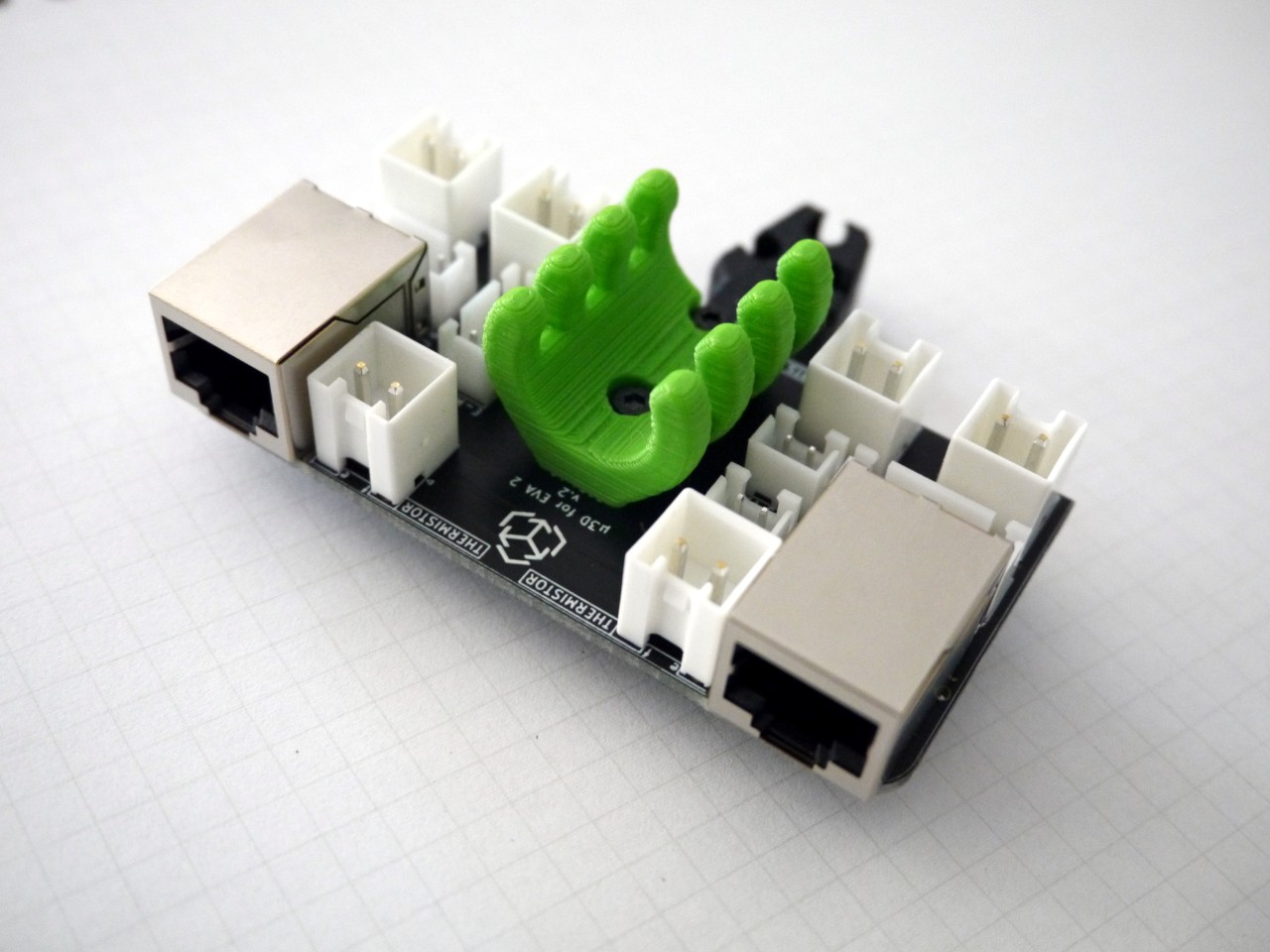
I've finally received the v.2 PCBs today, did some tests and can confirm they are acceptable.
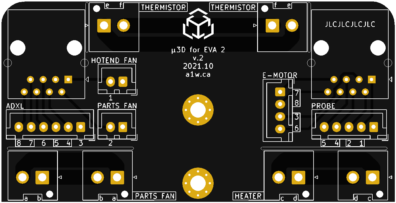
I did notice one minor mistake: pin 1 on the RJ45 below the KiCad logo is marked as GND but GND is actually pin 3. It can be quickly confirmed with an electrical continuity test.
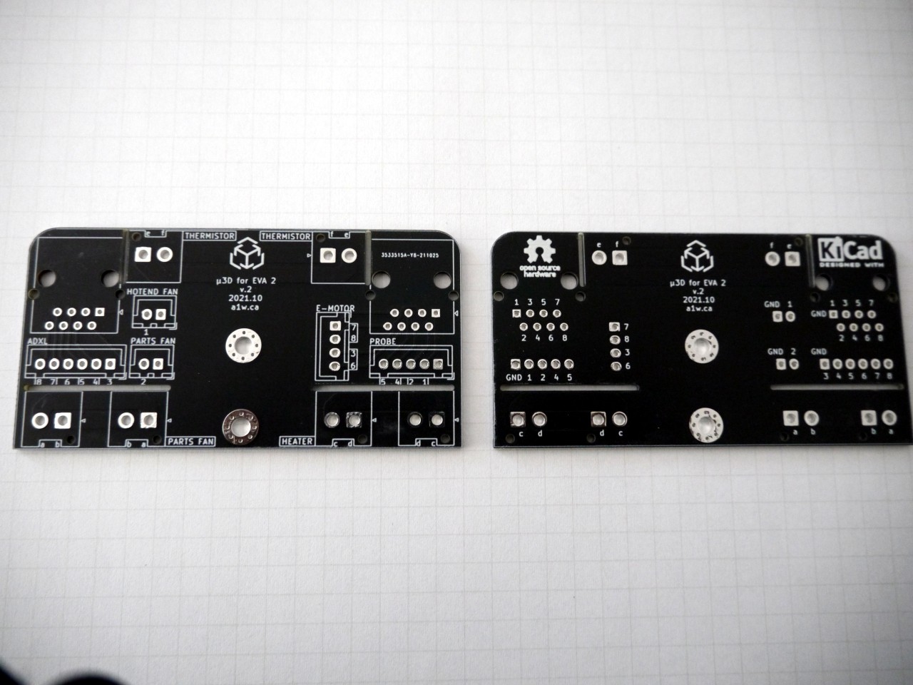
Despite the silkscreen error, everything works fine and the high current traces are tested up to 2A, even though the theoretical limit is much higher.
I am updating the documentation today and will publish v.2 for sale on Tindie hopefully by tomorrow.
Discussions
Become a Hackaday.io Member
Create an account to leave a comment. Already have an account? Log In.