Version 5
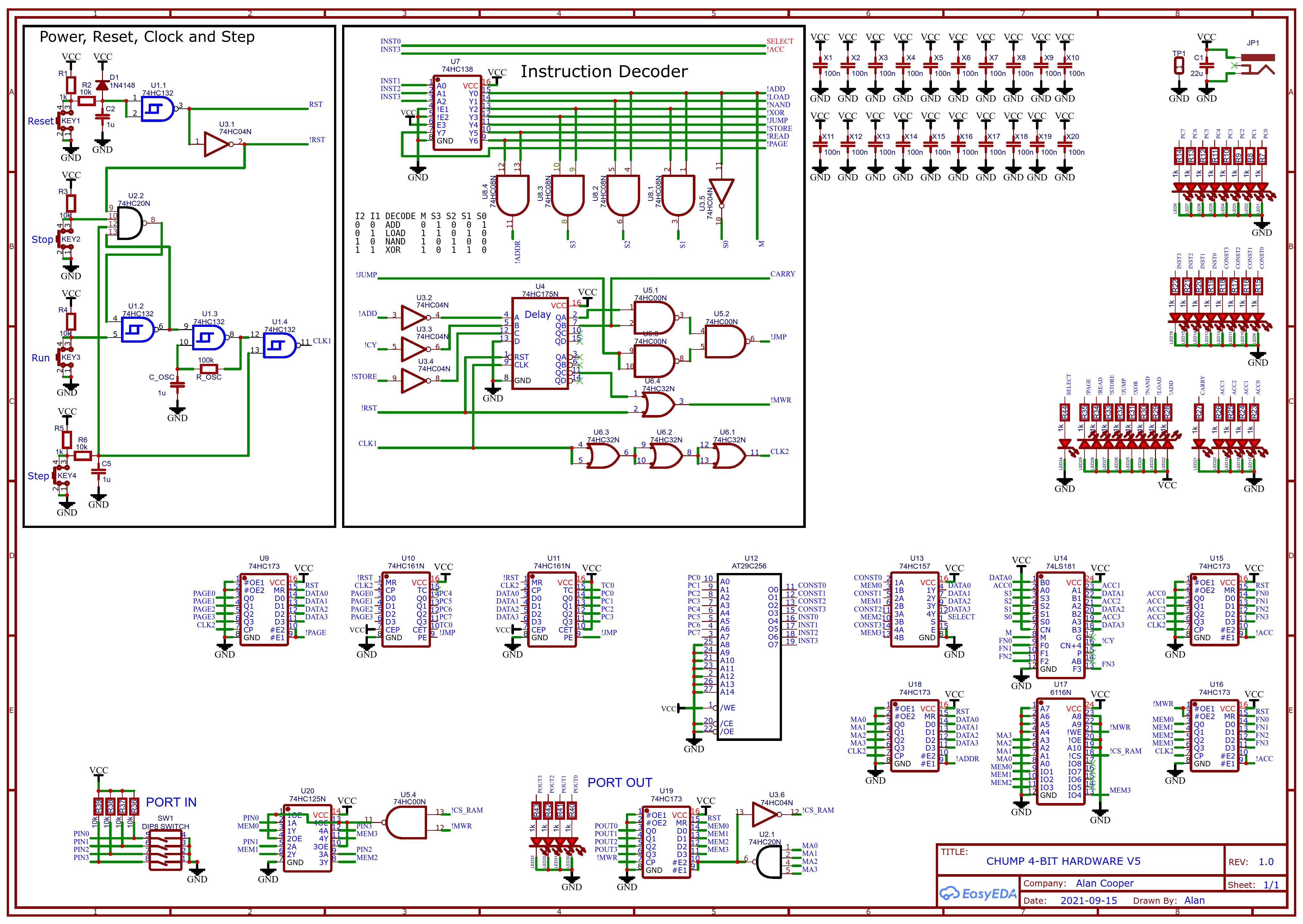
Version 4 did not last long! I have opted to use memory mapped Input/Output (IO) and an upgraded Reset/Clock/Step logic:
I have updated the LogiSim model as well:
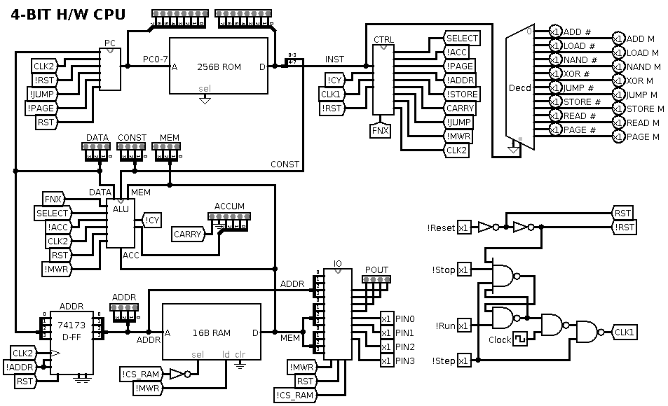
OpCode Improvements
Addressing the memory timing issues had the side effect of resolving post STORE issues. Now two STOREs can be sequential and reading memory after a STORE will return the stored value (which is the same as the ACCumulator value).
Input/Output Design
Here is the LogiSim IO design:
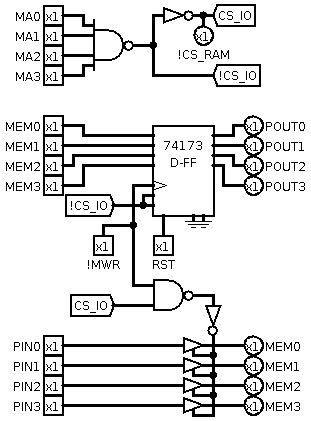
Note: Memory Address 0xF is now used for IO.
The PCB
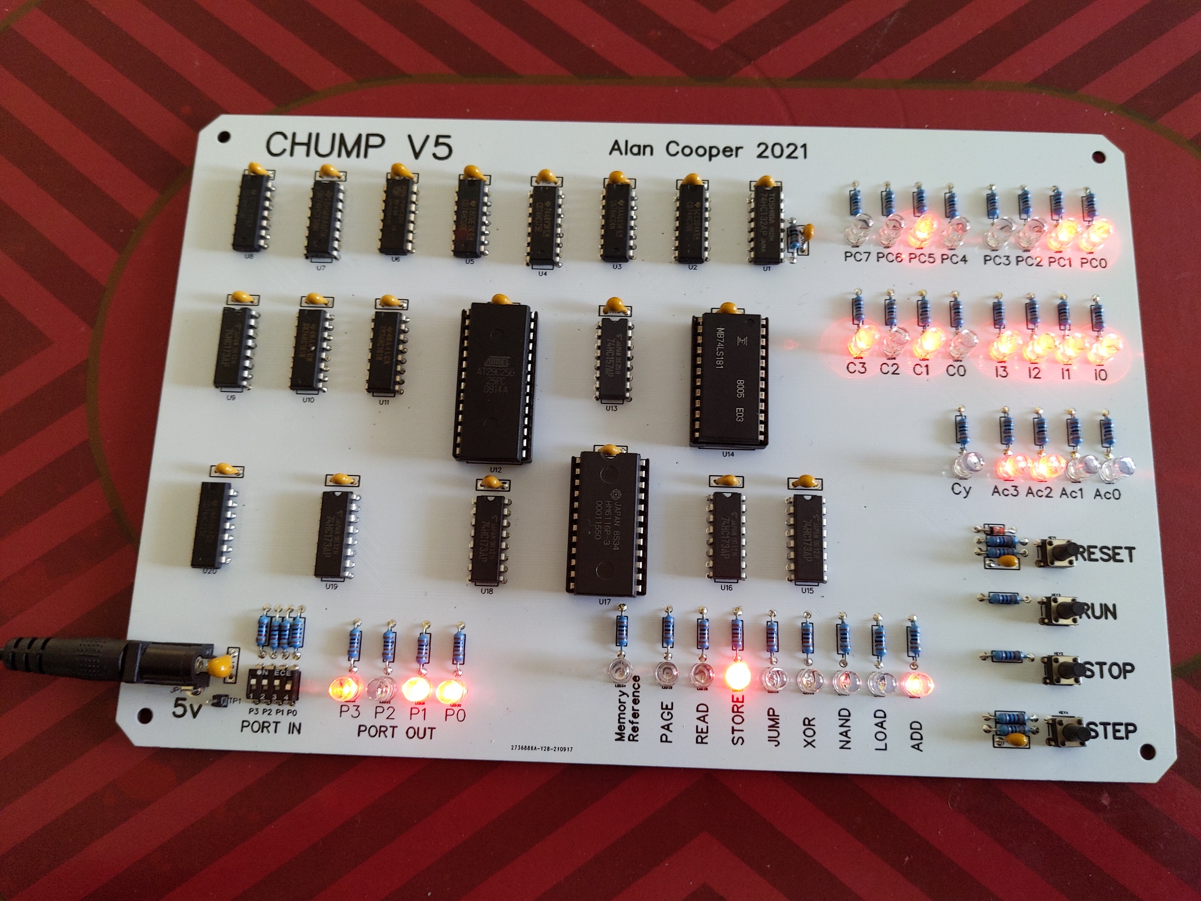
The PCB is now a little larger:
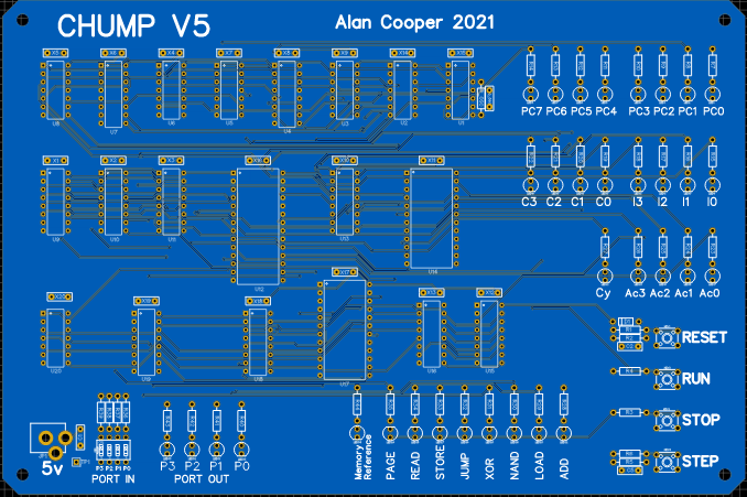
PCB Layout
The PCB is close to the point where the Easy EDA autorouter fails. I have a couple of strategies to extend the operational envelop of the autorouter:
- Adjust the track width (10 MIL) and clearance (9 MIL) to limit tracks between IC pins to one.
- Arrange the ICs to minimise connection lengths.
- Move ICs apart if track density is (too) high.
Assembly
Received the PCBabout a week ago. Assembled the PCB a few days ago. Wrote a test program this morning. Works fine. One minor problem was the Const/Inst labels are the wrong way around (I swapped the Const/Inst nibble order for V5).
Possible Upgrade
I think the ADD should be ADC (i.e. ADD with Carry) and the Carry should be persistent.
This would allow multi-nibble addition/subtraction without jumps. The carry signal can be cleared with "ADC 0".
Okay this project is done.
AlanX
 agp.cooper
Discussions
Become a Hackaday.io Member
Create an account to leave a comment. Already have an account? Log In.