Specifications
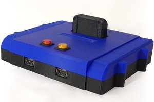
- 68000 CPU running at 10Mhz.
- 512K EEPROM
- 1M of Static RAM
- 8M Dynamic RAM
- 2 Serial ports
- Parallel port
- PS/2 keyboard and mouse
- IDE interface
- Real-time clock
- 4 Expansion slots
A Xilinx XC95108 CPLD is used for decoding logic and as a DRAM controller. Power is supplied using a standard ATX power supply.
 Stephen Moody


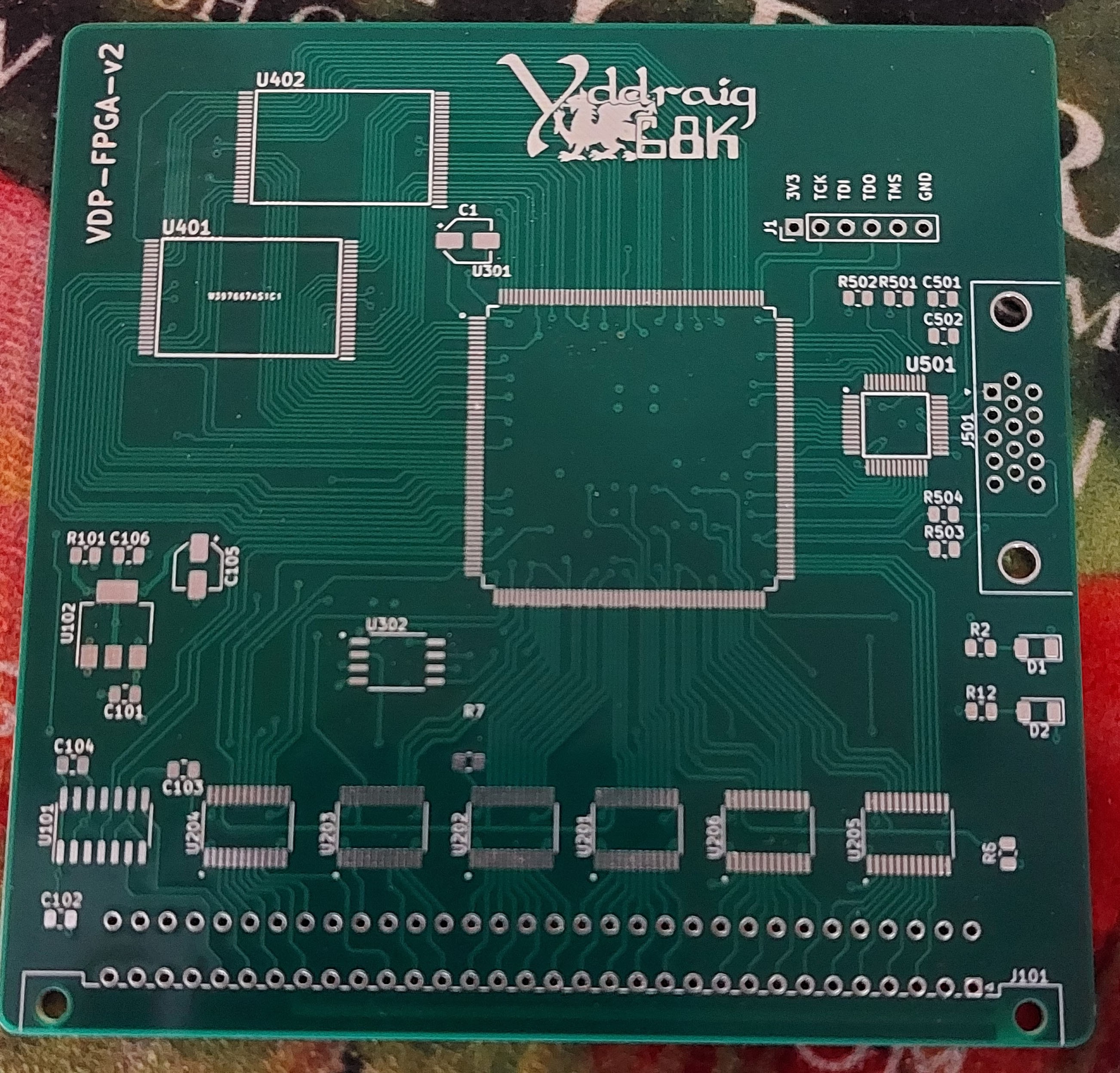
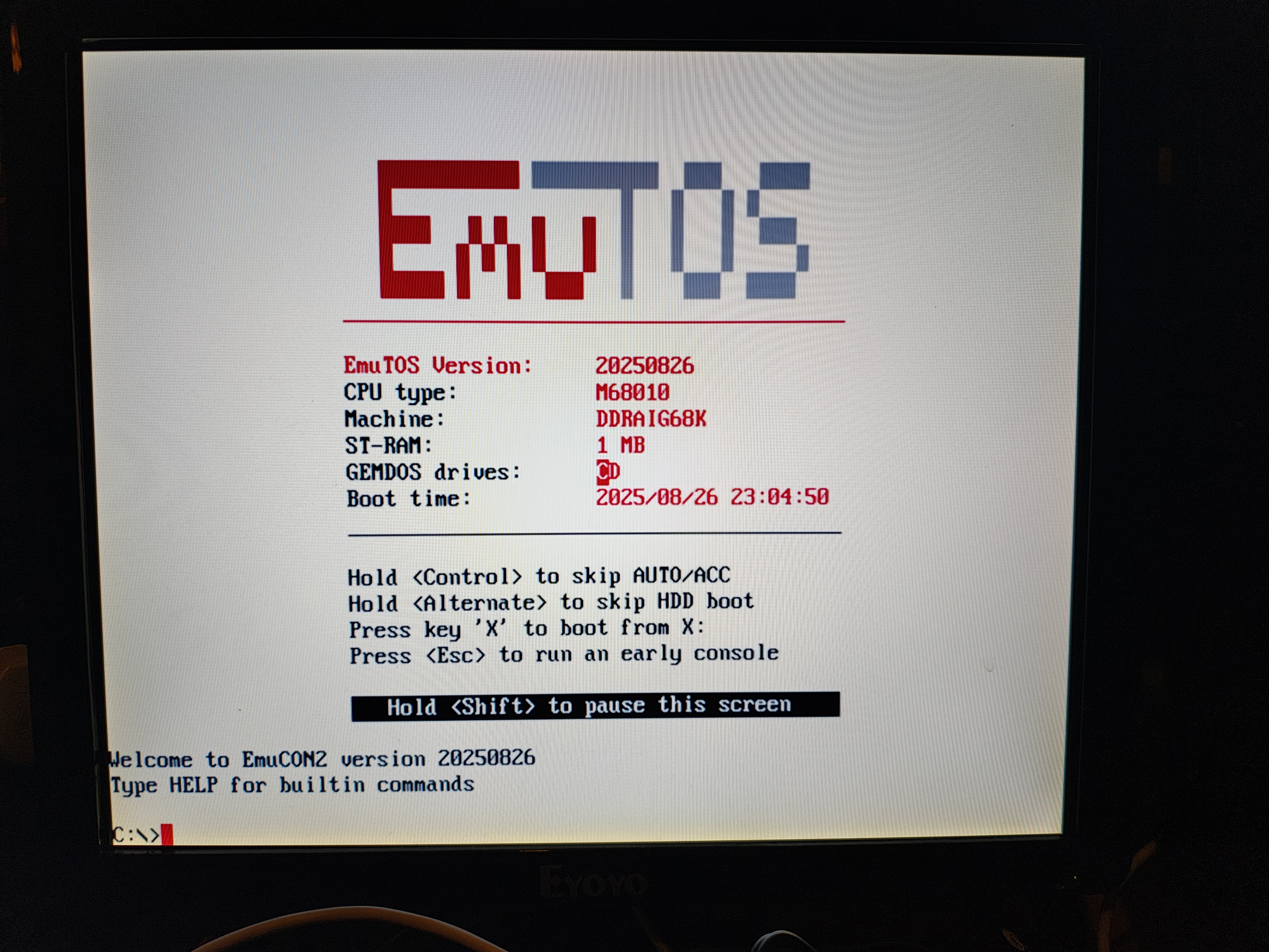 While that was working well, I wanted to get the desktop mode working. I ended up writing a fVDI driver for the VGA card. One good thing for starting with the fVDI diver is that it only needs a minimum of two functions, c_write_pixel and c_read_pixel to get it working. With those implemented I was able to get a working desktop up and running.



 Dylan Brophy
 Samuel A. Falvo II
 Clyde Shaffer
 Nicola Wrachien
Looks nice, great job!
But I can't stop thinking that it might have been better to have foregone on a few of the power lines in the busses and could have made the ram window larger than 1MB.
I was thinking about getting rid of one +12V line, because even with two +12V lines, the board can't deliver enough power for e.g. a harddisk. And all you might use the +12Vand -12V for would be for UART drivers.
Basically, I would shuffle A30 to C31 (removing one +12V), C30 to A2 (removing the GND), then move everything from A22 down one row, clearing up A22 and C22. Then move C21 (E) to C22. Then C21 can become 'A20' address and A22 can become 'A21' address. And then you can access 4MB per board.
This gives you the option to create 4MB ram boards. Which is memory that you will need very much if you want to do really interesting things with your VGA screen. ;)
You could also make your VGA with a 4MB ram window. Giving you the option of maybe making it kind of 'local' ram on the VGA chip. Accessible by CPU, but with low priority, CPU might have to wait. But accessible at full speed by the FPGA/VGA, giving you the option of fast blitting. While the CPU can continue doing its things until it wants to access the video ram again (and might have to wait a bit).
No worries, I'm just brainstorming. Your design is already great, and my ideas would increase the complexity really, really fast. ;)