 agp.cooper
LogiSim
Basically I am using SubLEq to teach myself LogiSim.
Is it even possible to get anything useful out of a 4 bit SubLEq.
Actually, yes I can get a 4 bit counter working in LogiSim.
74XXX Libraries
You will need some external 74XXX libraries. I used 74xx Libary.circ (https://github.com/kara-abdelaziz/CHUMP-processor/) and logi7400ic.circ (https://github.com/r0the/logi7400). Did not find a library that was complete.
I found and error in logi7400ic.circ for the 74161. The clock input was inverted. I modified my version of the library to fix it. Taking down this error took many hours.
From Concept to Working Simulation
I am impressed, about 15 hours over three days as a LogiSim novice.
Structure
LogiSim encourages the user to design your circuits hierarchically. Both with "bit width" and sub-circuits. As SubLEq is difficult to understand this is a good approach.
Programming SubLEq
Here is the binary counting program I am trying to implement:
| Address | A | B | C |
|
|
| 0 | 0 | 1 | 3 | Z = 0 |
P = 1 |
| 3 | 1 | 0 | 6 | Z = -1 |
|
| 6 | 0 | F | 9 | B = B + 1 |
|
| 9 | 0 | 0 | 3 | Z = 0 |
|
| C | 0 | 0 | 0 |
|
|
| F | 0 |
|
|
I/O |
|
Usually address -1 or in the case 0xF serves as Input/Output or output in this case.
Note: A write to the I/O address also write the value to memory.
SubLEq has only one instruction:
- Mem[B] = Mem[B] - Mem[A] and jump to C if the result is Less or Equal to zero.
Decoding the Binary Counter Program
Address Comment
0 0,1,3 ;Set up Z (=0) and P (=1)
Usually this is written:
0 0 1 ? ( ? means the very next address)
3 1 0 ? ( 1 is the count increment, set Z = -1 )
6 0 F ? ( Increment the output address 0xF )
9 0 0 3 ( Reset Z = 0 and jump to address 3 )
C 0 0 0 ( Not reachable but: Reset Z = 0 and jump to address 0 )
F 0 ( The I/O address )
I am sure you all got the above and can now program in SubLEq.
Where to Start?
The timing diagram. I can do this because I have a bit of an idea what the sub-system look like:

Lets put this into steps:
| Timing | Micro Code | Clock |
| T0 | MAR=M[PC] |
|
| T1 | ALU_A=M[MAR] | PC++ |
| T2 | MAR=M[PC] |
|
| T3 | ALU_B=M[MAR] |
|
| T4 | M[MAR]=ALU_OUT; !WE; | PC++ |
| T5 | IF (LEQ) THEN PC=M[PC] ELSE PC++ |
|
Don't be misled, although I present a linear process, it is still iterative.
The ALU
The ALU is fairly simple:
Subtract: B = B - A
Flag: !LEq
Therefore we need:
- Load A: !ALU_LDA
- Load B: !ALU_LDB
- Read B - A: !ALU_OUT
And because of the type of control logic I am using:
- Clock: CLK
- Reset: RST
Here is my schematic:

Chip Count:
- 2x 74HC173
- 2x 74HC283
- 1x 74HC04
- 1x 74HC125 (the inverter and tri-state output buffers)
The beauty of LogiSim is that you can test the sub-circuit before proceeding.
Program Counter
The program counter is perhaps the simplest sub-circuit to design. Note: the outputs PC0-3, these are for debuging LED display in the top level:

Note: the 74161 in the logi7400ic.circ library has the clock inverted. I have edited my version of the library.
Memory Address Register (MAR)
The idea behind the MAR is to load a value from memory and then use that value as an address to load an indirect memory value. Thus it is a form a indirect addressing.

Note: the MAR0-3 outputs are for debugging.
Output
Output for SubLEq is a little tricky, I have solved this by shadowing a memory location (-1 or 0xF) for the output register. So reading the output just returns the value stored in memory during the write to the port.

Input
Don't need an input for this demonstration computer but if required it would be mapped to -2 or 0xE. The memory location would be need to be disabled.
The Control Logic
Now that the main sub-circuits have been designed and there control signal named we can map the timing diagram to logic:
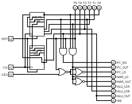
The core of the control logic is a Johnson counter (2x74HC175) setup to cycle a six state low bit (for T0):
- T0 T1 T2 T3 T4 T5
- 0 1 1 1 1 1
Reading the timing table !PC_EN (enable the PC count), a 3 input AND gate on T1, T4 and T5 will meet the control specification:

With all the control systems I have played with this is absolutely the simplest (I have come across).
The Top Level Circuit
Here is the top level circuit:
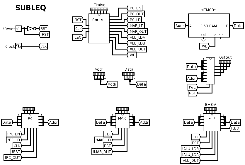
As you can see I don't bother connecting the sub-circuits up to each other via wires. Just use the "tunnels". If you didn't know, if you hover the mouse over the sub-circuit pin it tells you the pin name.
The Simulation
And here is the simulation:
https://cdn.hackaday.io/files/1816007769574400/4Bit_SubLEq-2021-09-08.mkv
AlanX