f4hdk
f4hdk-
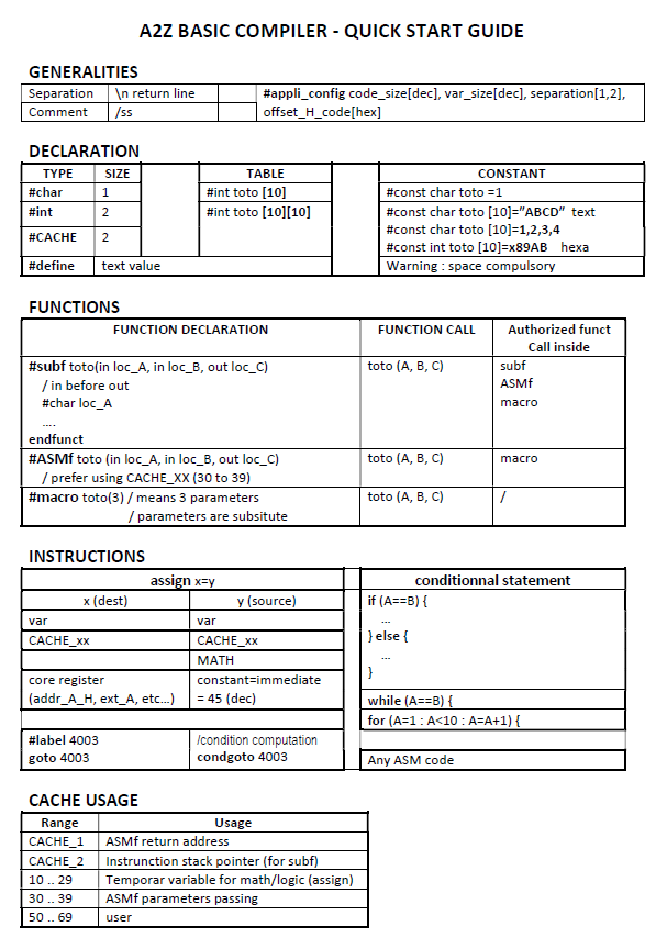
3.2) A2Z_Basic Language
11/13/2016 at 18:15 • 0 commentsA2Z Basic is a language invented by myself. I wanted something slightly different from existing languages, primarily for fun, but also to help the compiler. The syntax is closed to C, but much less rich.
Be careful : if you code in A2Z Basic, there are lots of constraints that exist just to make the job easier for the compiler. For example, each instruction must be in a new line, including closing accolades.
If you want to copy the result of a computation in a variable, you must use the instruction “assign” before the formula.
Finally, the compiler is not smart, and it is not able to prioritize math or logic operations inside a complex expression. You must put parenthesis everywhere, in order to split each elementary computation.
if ( ((Xm_pos//4) >= 128 ) & ((Ym_pos//4) >= 32 ) ) {
If you don’t respect these rules, there will probably be no error message from the compiler, but the executable code generated will not work.
You can integrate assembly code directly in the middle of A2Z Basic code. This is used to code low level functions, to access hardware directly (drivers).
The directive #appli_config sets the maximum allowed size for code and variables, and the position of the generated file inside RAM. The RAM portion dedicated to variables can be common (separation = 1) or separated (separation = 2) from the executable code. With option 2, you can use the full range 64kB for variables.
![]()
Functions:
There are 3 types of “functions”:
- Subf : these are classic sub-functions which calling is managed on the execution stack.
- ASMf: so called ASM function. They are elementary, low level function that cannot call other functions. The return address is not stored in the stack, but in a specific CACHE position. The calling and return of ASMf are therefore much faster than for Subf. This is useful for repetitive functions called very often.
- Marcos: macros are pieces of repetitive code that are just substituted inside the source code before its parsing
Limitations of the language and the compiler
- Static memory allocation, no dynamic memory allocation (no data stack or heap).
- No recursive functions management : a function cannot call itself, either directly or indirectly, because of the previous limitation (static memory allocation)
- 64kB only of memory range for variables, because of 16bits pointers. But a program can access the whole 2MB range with low level instructions
- 2 dimension tables at maximum
- Only 1 basic source code file at input of the compiler. No “include”, no library (static or dynamic). All functions used in a program must be copied to the source code, even repetitive functions (printf)
-
3.1) Software development tools
11/13/2016 at 18:15 • 0 commentsThese software tools are 100% homemade; they are written in C, for Windows, compiled with Visual Studio Express 2013. The code is probably portable to other platforms.
All source and executable are given “AS IS” without any licence. I have to admit that I don’t understand all these open source licences.
Warning : the code might probably look ugly, with lots of global variables. It is not academic, but it works. I am almost autodidact.
On Windows, you will probably need to install Visual Studio 2013 redistributable package![]()
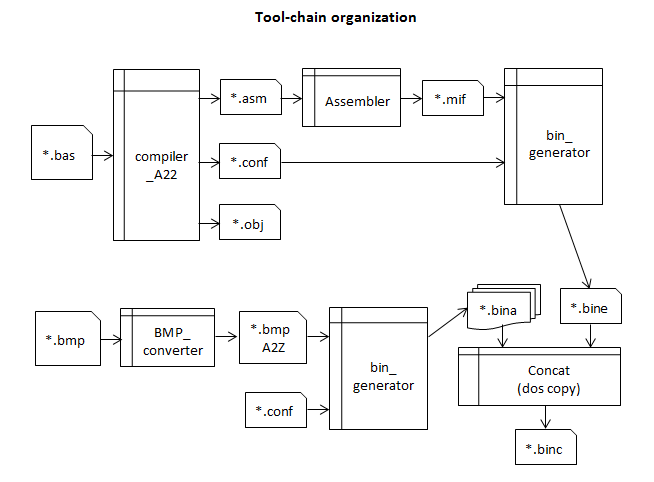
Files extensions of the tool chain:
- .bas : source code written in A2Z Basic
- .obj : a text list of all declaration of functions and variable, and their allocation to memory. Just for debugging by hand.
- .asm : assembly code
- .conf: configuration for the “bin generator”. It contains the size and RAM address of the data to transfer.
- .bina : binary data file to transfer to A2Z, it uses the bootloader protocol
- .bine : binary executable file to transfer to A2Z, it uses the bootloader protocol
- .binc : concatenation of one .bine file, and one or several .bina
- .bmpA2Z : intermediate format for bitmap images generation
-
2.5) FPGA-Verilog: other peripherals
11/13/2016 at 18:11 • 0 commentsBoot ROM:
This is in fact a 2kB RAM, inside the FPGA. This is the very first peripheral that I have used for debugging the core. I have put the very first programs in this little memory. The tool “in system memory content editor” from ALTERA allow to read or write in real time, like a RAM/EPROM emulator. The content can also be written by the CPU, for debugging purpose.
PS2 keyboard:
I have made errors on this part, which is more complex than needed. But it works.
The CPU cannot handle interrupts. Therefore, I have integrated a small FIFO between the PS/2 and the CPU, so that the computer doesn’t miss any information from the PS2.
There is 1 flag to indicate that the FIFO contains unread data.
Serial interface:
There is no real serial interface, but just a GPIO port : 2 bits inputs and 2 bits output.
The serial port is emulated in software via a bit-banging method. I have only coded the RX part (from PC to A2Z), for downloading content to A2Z.
The choice of bit-banging is questionable : it is very slow, and limits the baudrate to 56kbps. This is not reliable above.
Downloading a 1MB file at 56kbps is very very slow. I could have made 10 times faster with a hardware serial port.
SPI interface:
The FPGA integrates an SPI master interface.
There is only 1 peripheral connected to this SPI : 16MB of Flash memory.
The configuration is fixed : 8 bits transfers, 12.5MHz.
There are 2 shift register, one for the MISO and one for MOSI. The address of this peripheral is the same for both reading and writing to the SPI, even if the registers are physically different. The goal is to reduce the instruction count, and to avoid switching the address.
Each write instruction to this address triggers a transaction of 8 bits, that involve both MOSI and MISO buffers. The MISO buffer is therefore also filled just after a transaction triggered by a write order to the MOSI buffer.
-
2.4) FPGA-Verilog: VGA video card
11/13/2016 at 18:10 • 0 commentsThe hardware integrates a VGA video card, that generates a VGA signal of 640x480 60Hz.
The signal is generated with 2 parts
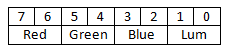
1) Graphic part, 256 colors:
The palette is fixed : 2 bits out of 8 are dedicated to brightness, and 2 bits for each of 3 colors.
The palette part directly feeds 3 discrete digital to analog converters, made with discrete resistors.![]()
The video memory is shared with the CPU, inside the 2MB SRAM. 50% of the time is dedicated to the CPU, and 50% is dedicated to this graphic part.
The video card integrates a double buffering mechanism, for fluid animations.
Once the software requests a video buffer switch, the hardware waits for vertical synchro and then switches from one frame buffer to the other.
There is no hardware acceleration inside the “VGA graphic card” (like sprite management). All graphics are generated by software only.2) Text part:
The text is overlaid over the graphic. There are 80 columns x 30 lines of characters. This is very helpful for debugging the computer, and for coding the first programs with a simple text output.
Synchronization:
The 3 parts (CPU, VGA graphics, VGA text) need to be precisely synchronised with each other. When I programmed this, I only had little experience of FPGA and Verilog, and therefore it was a difficult part for me.
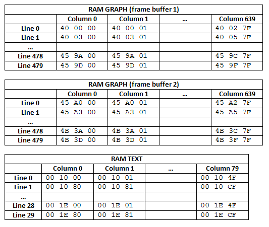
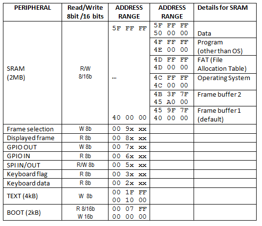
Address mapping of VGA
![]()
-
2.3) FPGA-Verilog: the core
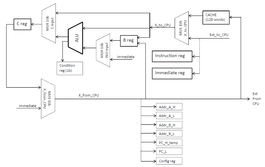
11/13/2016 at 18:10 • 0 commentsThis is a 16 bits RISC CPU, with a very simple instruction decoding.
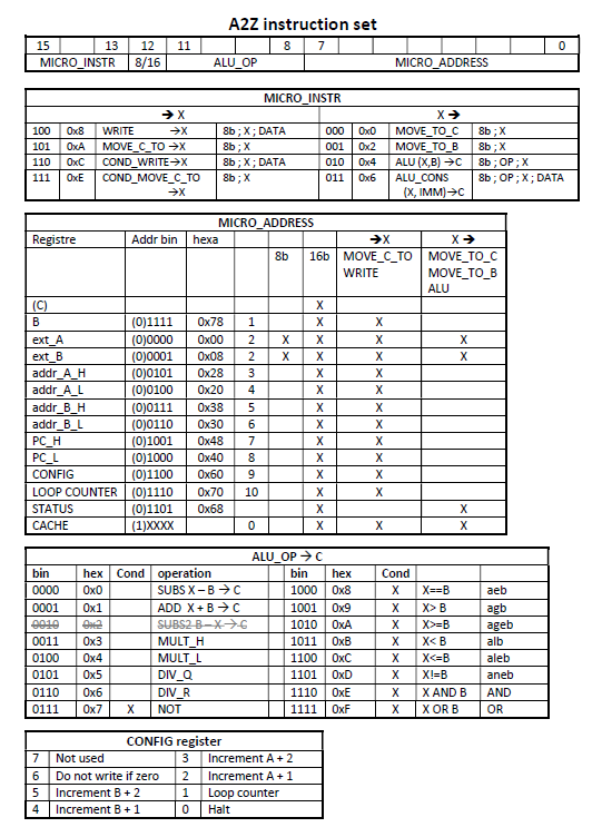
There is no microcode. Each instruction is very simple, very basic. The complexity usually found in the microcode is transferred to the compiler. The compiler has to generate a complex sequence of simple instructions. The execution code generated is therefore quite huge, but this is not a problem with 2MB of RAM.
The datapath of the CPU-core is mainly “load and store”, and the register C is the central register.
![]()
Some instruction can take 16bits of optional “immediate” value, written inside the code.
Therefore, one instruction can take 1 or 2x 16bits of executable code size.
The ALU only computes integers, which is enough for this computer.
![]()
CACHE :
1 have put a 128x16bits cache memory inside the FPGA. This cache can be accessed directly with one instruction : the 7-bits address of this cache memory is mapped to the last 16bits of the instruction.
This greatly accelerates access to intermediate data when computing. The compiler uses this cache systematically for intermediate variable of complex formulas.
But this cache memory is accessed at the same speed than external memory. I could have made this with a “zero page”, but at the beginning of the project, I didn’t know this concept.
Optimizations
3 hardware optimisations are available inside the core, which accelerate data copy and sprite manipulations. My first goal was to make 2D graphic games.
These 3 mechanisms are optionally activated via the “config” register of the core.
The compiler is not able to use these options naturally, and the only way to use them is to code in assembly language.
The 3 optimisations are:
- Hardware loop counter : repetitive loops can be counted in hardware, and the stop condition is computed in hardware, not in software. This is like a “for-next” loop, but faster. The loop counter is decremented at each call of one “goto” instruction. The initial value of “loop counter” (the number of occurrence of loop) shall be written in the “loop counter” register.
- There are 2 separated address registers for data manipulation (A and B), each with a post-increment option. The post-increment can be +1 or +2, to adjust to a word size of 8bits or 16bits. All this help to copy data from one address range to another.
- The last option is “do not copy if zero”, in hardware. This is helpful for transparent sprites. The colour 0x00 means “transparent”
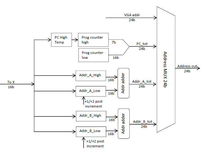
Address computation :
![]()
The 24bits address are computed in hardware with a sum of 2 16bits address registers called address low and address high. This helps for manipulating big tables and 2D images. The address high is dedicated to the line address, and address low is dedicated to row address.
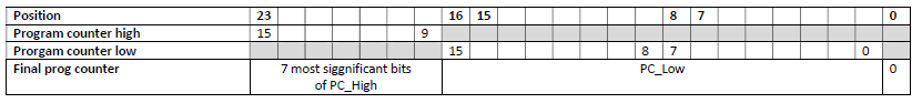
For the program counter, there is no sum mechanism, because it would be useless. Every program remains within 128kB of memory, which is more than necessary.![]()
![]()
Warning, address manipulated by the program counter manage words in 16bits, omitting the last address bit, unlike data which address are expressed in 8 bits words, whatever their size.
Errors:
The core of the CPU is the first part that I have coded (remember, this is my first FPGA project). I have made quite a lot of errors. This could have made the core compute faster.
The “load and store” architecture is too simple. There is no reason to make such architecture in an FPGA.
I also have integrated a 16bits hardware divider. This is almost useless, and consumes lots of FPGA cells.
When I started this project, I was only little aware of all these aspects, and I learned them while working on it. I discovered these errors too late, while coding the compiler, and I didn’t want to reorganize the project.
-
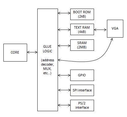
2.2) FPGA-Verilog: global overview
11/13/2016 at 18:09 • 0 comments![]()
The CPU is a “Von Neumann” one (as opposed to Harvard), for simplicity. There is only one external bus (data + address), for all memory and peripherals.
![]()
The 16bits words are organized as “little endian”, because I think that it is logic.
Frequency:
The biggest frustration of this project is the frequency. Theoretically, the CPU could have run at 50MHz. At this frequency, 3/4 of the time is dedicated to the CPU for computing, and 1/4 of the time is dedicated to the VGA. Therefore, the CPU is equivalent to 37MHz.
But I had lots of difficulties to understand FPGA timing constraints. I am 100% autodidact, and this my first FPGA project. The FPGA was not reliable at 50MHz, and I was stuck 2 months trying to solve this problem.
I wanted to go on with other parts of the project, and not remain stuck. That’s why I decided to reduce drastically the frequency to 25MHz. At this frequency, 1/2 of the time is for the CPU, and 1/2 for the VGA. This is equivalent to 12Mhz, and global performances are divided by 3.
This is a big disappointment.
8bits – 16bits:
Warning, data can be manipulated with 8 bits or 16 bits.
But among all the peripherals mapped to the address plan, only the SRAM can be accessed via 8 or 16 bits.
The boot Rom (in reality this is a RAM) can only be accessed with 16bits.
The text RAM only accepts 8bits access, and can only be written by the CPU, not read.
The SPI is 8 bits only.
There is no protection in the compiler, and it is easy to make errors.
-
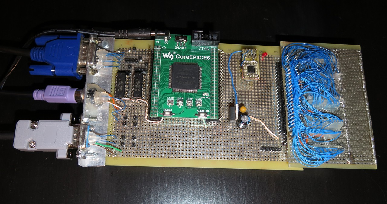
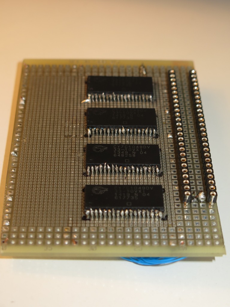
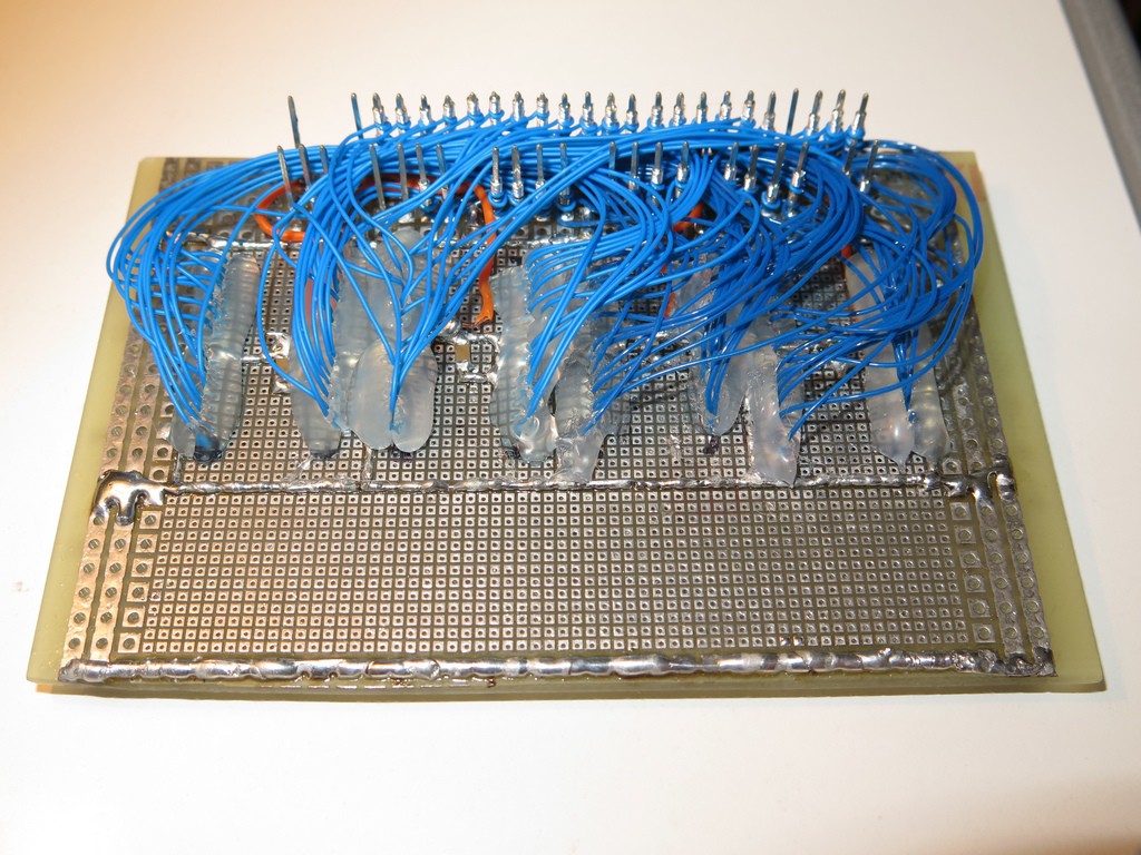
2.1) The FPGA development board
11/13/2016 at 18:09 • 0 commentsI have built this development board by myself, using wrapping technique, because I couldn’t find any board with 2MB of SRAM arranged in 16bits. I wanted SRAM, instead of DRAM, for the simplicity.
I also have to admit that I like soldering and wrapping. For me, an electronic project must contain soldering, and otherwise it would not be fun.
Main components used:
- FPGA : Wave Share Core EP4CE6 breakout board (ALTERA Cyclone IV FPGA with 6000 logic cells)
- SRAM : 4 x CY7C1049 (512k x 8 bits)
- FLASH : Micron N25Q128A (16MB)
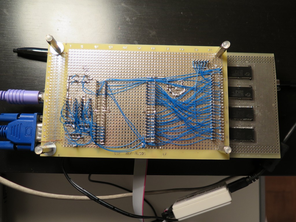
Wiring table (sorry, awfull scan)
![]()
![]()
For SRAM chips, I have used SMD. The 30AWG wires are soldered on the SRAM side, and wrapped around the pins on the other side. The wiring of the SRAM board is quite dense, with more than 120 wires.
![]()
![]()
But making this board is only a very small portion of the project. Most of the complexity of the “hardware” is hidden inside the FPGA, in the Verilog code, described in the following chapters.
-
1.2) Personnal vision of the project
11/13/2016 at 18:08 • 0 commentsFor me, it is really an exciting project.
This project contains lots of different topics, and therefore it is not monotonous at all.
I have learned a lot with this project. I have discovered Verilog language, and I have learned how a compiler is made. This requires quite a lot of thinking.
The main goal of the project is to manage quite all the parts of a computer. I am proud of this aspect.
It is an old dream, which started when I was young: understanding in details all the part of one computer, and if possible build one by myself, from scratch, from A to Z.
I programmed in 3 different languages for this project: Verilog, C, and A2Z_Basic (my own invented language).
This project is quite big (for me), and therefore, it needs a good organisation. I needed to split it in small parts. This is a long project, which needs a lot of time and motivation.
But his project is feasible, even if it is long. Once it is split in several parts, each part is not so hard… except from the compiler which is the most complex part (for me).
Once a part is coded and debugged, you can often rely on it, almost forget it, and develop the new layer above. This stack of (relatively) simple layers makes a full computer. Of course, I often discovered some bug in one under layer, while developing the above layer. But I always came to a point where I can declare that one layer is reliable.
I am really proud of this project, and especially in developing it 100% by myself, as an autodidact, from A to Z.
-
1.1) Principle of the project
11/13/2016 at 16:19 • 0 commentsA2Z computer is a computer imagined by me, designed by me, and made by me. It is made from scratch, from A to Z.
It is a didactic project. A "learning by doing" project. The goal is to learn and understand in details all the aspects of a simple computer, including hardware (CPU and peripherals), soft dev toolchain, and software itself. This computer is very simple, not efficient (16bits CPU, 2MB of RAM), but it works!
Every part of this project is invented, designed by myself. I have not copied any line of code from another project. I have coded in 3 languages : Verilog for the hardware, C for the software development tools, and A2Z_Basic (my own basic language) for the applications.
I have not ported any open source code.
The only thing that I have copied from existing source is the text font, because it would have been tedious to do it by myself pixel per pixel.
The goal is really to do everything from zero.
The project is also not intended to imitate an old CPU architecture. This is not a vintage computer.
It is not aimed to be an usable, every-day computer, or to run Linux or so (take a look at the Kestrel project for that).
I have used “modern tools”. Therefore, the project is not an attempt to imitate the work of the microcomputer pioneers (Steve Wozniac or so). I have used the following modern tools:
- A PC as main development tool
- One FPGA (Altera Cyclone 4) and its development software Quartus II
- A logic analyser
- The A2Z tool chain works on a PC (Windows), and is coded in C, with Visual Studio Express
Warning:
This is an amateur project. I am autodidact. Lots of things inside this project are not optimal, not academic. Every part is quite simple and with very little optimisation. The result is quite good for me, but I have made quite lots of errors, design errors, and simplifications. Remember : I am autodidact, and I am not a computer scientist at all.
This is also my very first FPGA project, my first Verilog project. I have learned the Verilog language by myself especially for this project.
Therefore, if you copy-paste this project for your university project, you can get low grade.
This website describes all the work that I have done, and it is also a user guide if you want to play with it.
I have tried to give all useful information. But if you think that something is missing, do not hesitate to ask it to me.
A2Z Computer
A computer invented, designed and built from scratch. Custom CPU on FPGA.