 Yann Guidon / YGDES
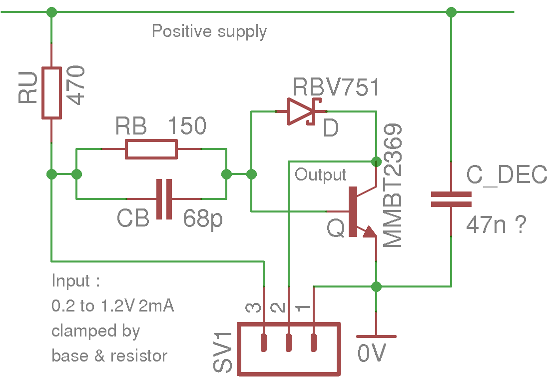
DCTL originally meant "Direct Coupled Transistor Logic", as described by @Tim on his great pages about the CDC6600 technology.
I have tried to increase the speed/power ratio with the help of a finely tuned base capacitor (C) and a Baker clamp diode (D) which seems to provide a propagation time of 2ns per inverter and/or a much better low-power performance. So this gives a new meaning to DCTL : Diode Capacitor Transistor Logic.
It's pretty easy to use yet quite unusual because each gate is only an inverter that provides an open-collector output, so it's all "OR-tied" logic, there is no dedicated inputs for each signal.
I have presented/introduced the individual gate in the description page of the project:
I have worked a bit more to make the PCB more compact:
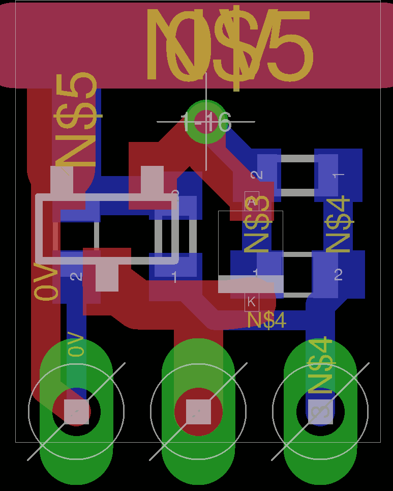
There is only one via now, and all the passives are on the bottom layer, which could be pick&placed by machines. Here I only use 0603 parts but they could be changed to 0402 or anything you want.
Here are the top and bottom layouts:
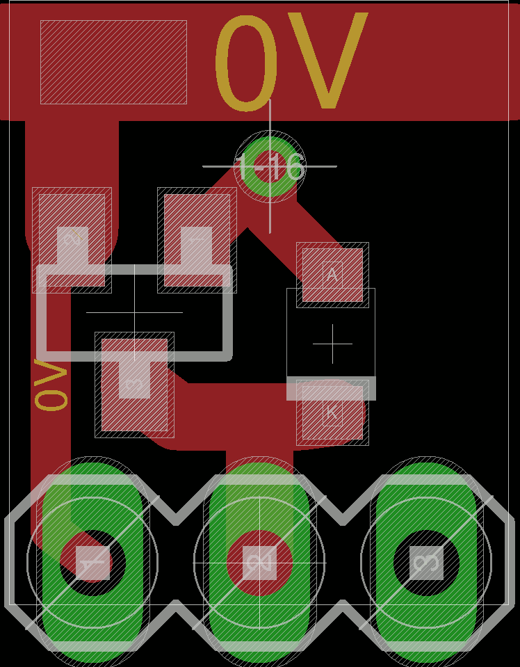
Now, the Ground/0V rail is on the top layer and directly connected to the PMBT2369's emitter.
There is some room at the right of the clamp diode.
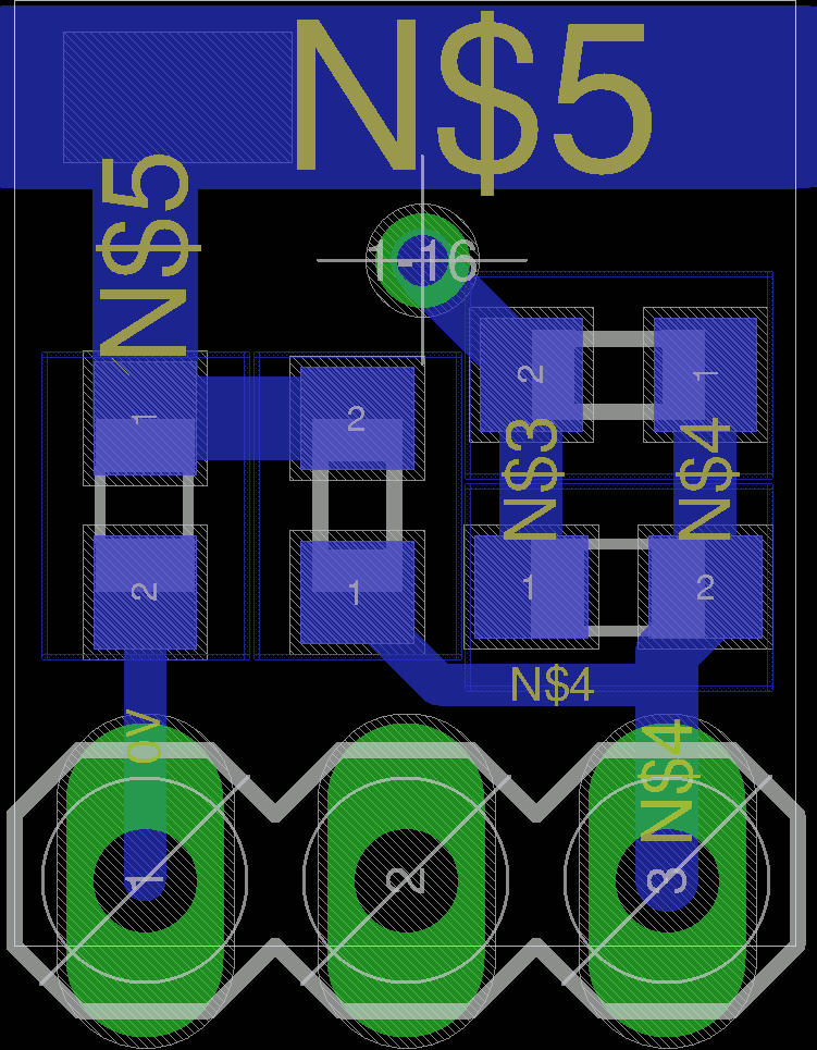
The bottom layer has the passives (2 cap, 2 res) and the Vcc supply rail.
I added windows on the rails to make them easier to solder to sources/supplies.
Overall I have tried to reduce the "height" of the gate, compared to the first version. This makes the strips more densely packed and more cost-effective.
Discussions
Become a Hackaday.io Member
Create an account to leave a comment. Already have an account? Log In.