 AlliedEnvy
To get started, we need to understand the 555 from a digital logic point of view.
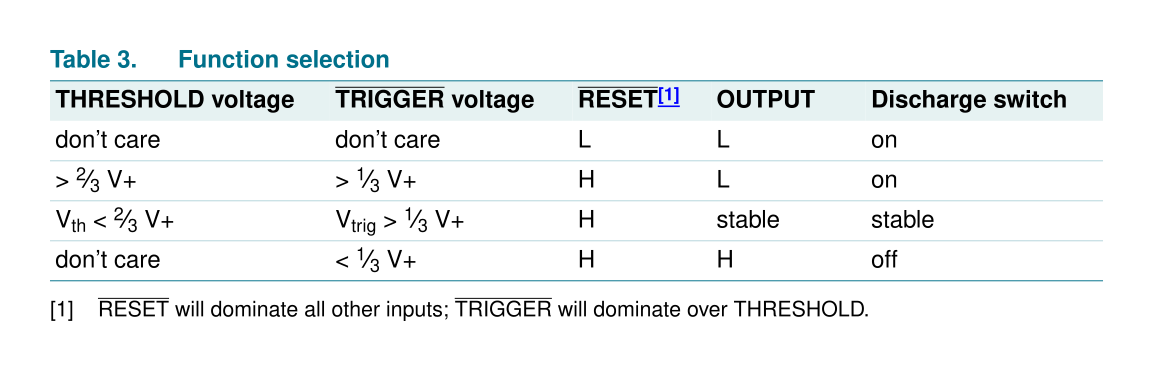
Throughout the project, I will refer to the ICM7555 datasheet1 from NXP (nee Philips Semiconductors, nee Signetics, the originators of the 555).
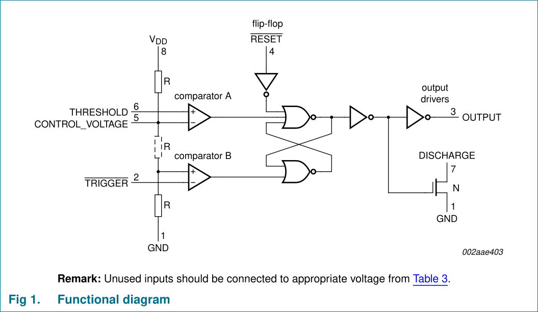
From the functional diagram, the 555 can be thought of as a circuit with 3 stages, each feeding into the next:
- A combinational circuit with 4 inputs (one tristate) and 2 outputs.
- An RS latch (the cross-coupled NOR gates in the center).
- 2 output drivers.
Most of our analysis will be on the first stage, so let's get the other two out of the way.
The RS latch has its S (set) and R (reset) inputs coming from stage 1, and its Q and !Q outputs go to the output drivers.
The two output pins are Output, a push-pull output driven by Q, and Discharge, an open-collector NPN/N-channel transistor driven by !Q. Discharge can sink a modestly larger amount of current compared to the rest of the pins.
This leaves the combinational input stage 1. There are 4 input pins: !Reset, Threshold, !Trigger, and Control (Control being tristate). An exclamation mark (!) or overline in the diagram indicates the input is active-low.
To simplify analysis, we will split Control into two inputs, Control and Control-Enable. When Control-Enable is low, Control is inactive, floating in high-Z state. When Control-Enable is high, the Control pin being actively driven high or low.
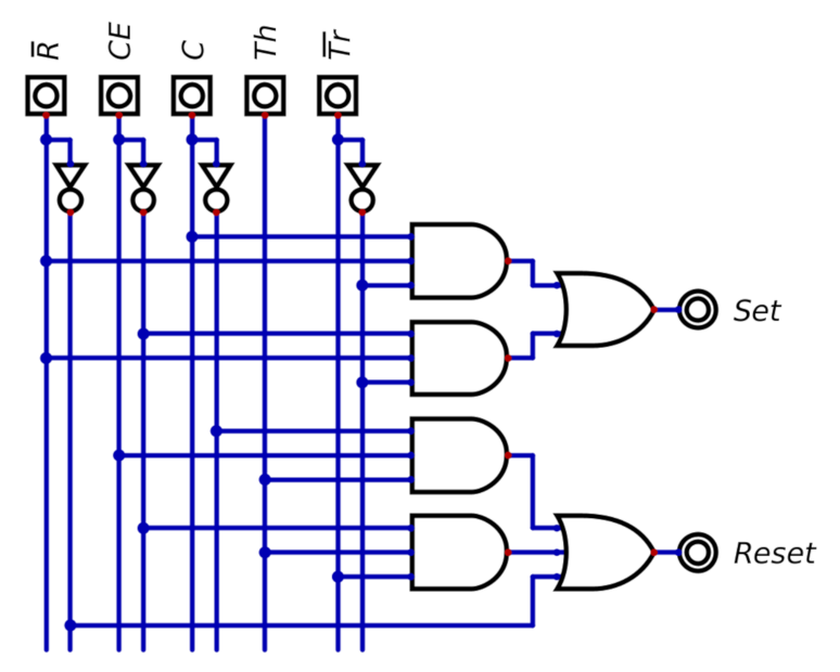
Now we have 5 inputs, for a total of 32 (25) items in our truth table to suss out.
From the functional diagram, we see Control has an effect on Threshold and !Trigger, but not !Reset. And from the function selection table, !Reset overrides all other inputs. So 16 of our truth table are:
| !R | CE | C | Th | !Tr | Set | Reset |
|---|---|---|---|---|---|---|
| 0 | x | x | x | x | 0 | 1 |
Considering Control as disabled, our next rows from the function selection table are (giving another 8 entries in the truth table):
| !R | CE | C | Th | !Tr | Set | Reset |
|---|---|---|---|---|---|---|
| 1 | 0 | x | 1 | 1 | 0 | 1 |
| 1 | 0 | x | 0 | 1 | 0 | 0 |
| 1 | 0 | x | x | 0 | 1 | 0 |
This leaves 8 states with CE enabled; 4 with C low and 4 with C high. Some experimentation and study of the functional diagram reveals that when C is low, !Tr is disabled, and when C is high, Th is disabled. Our remaining rows are:
| !R | CE | C | Th | !Tr | Set | Reset |
|---|---|---|---|---|---|---|
| 1 | 1 | 0 | 0 | x | 0 | 0 |
| 1 | 1 | 0 | 1 | x | 0 | 1 |
| 1 | 1 | 1 | x | 0 | 1 | 0 |
| 1 | 1 | 1 | x | 1 | 0 | 0 |
Plugging this into Digital, we can synthesize a circuit from the truth table for simulation:
Adding some circuitry to make CE from C, the remaining stages, and some delays to make changes propagate at the same time, I get:
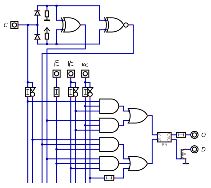
This is the model I'll be using to design the clock.
[1] This is their CMOS 555; I couldn't find a bipolar 555 datasheet on NXP's site, but I'll be designing towards the CMOS 555 anyway.
Discussions
Become a Hackaday.io Member
Create an account to leave a comment. Already have an account? Log In.