 Jesse Farrell
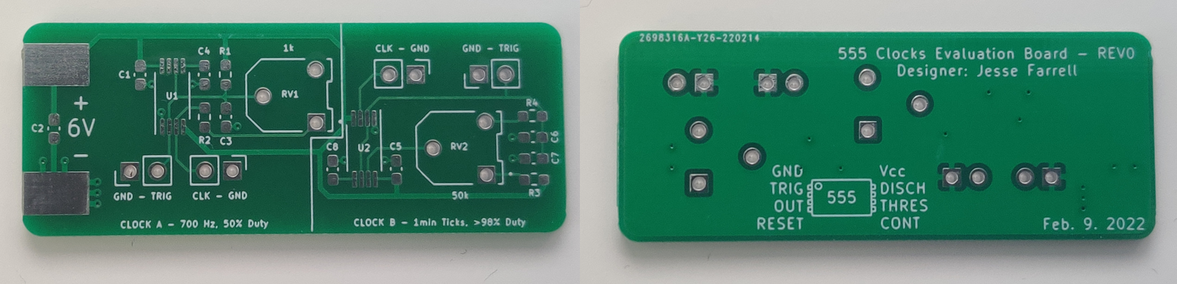
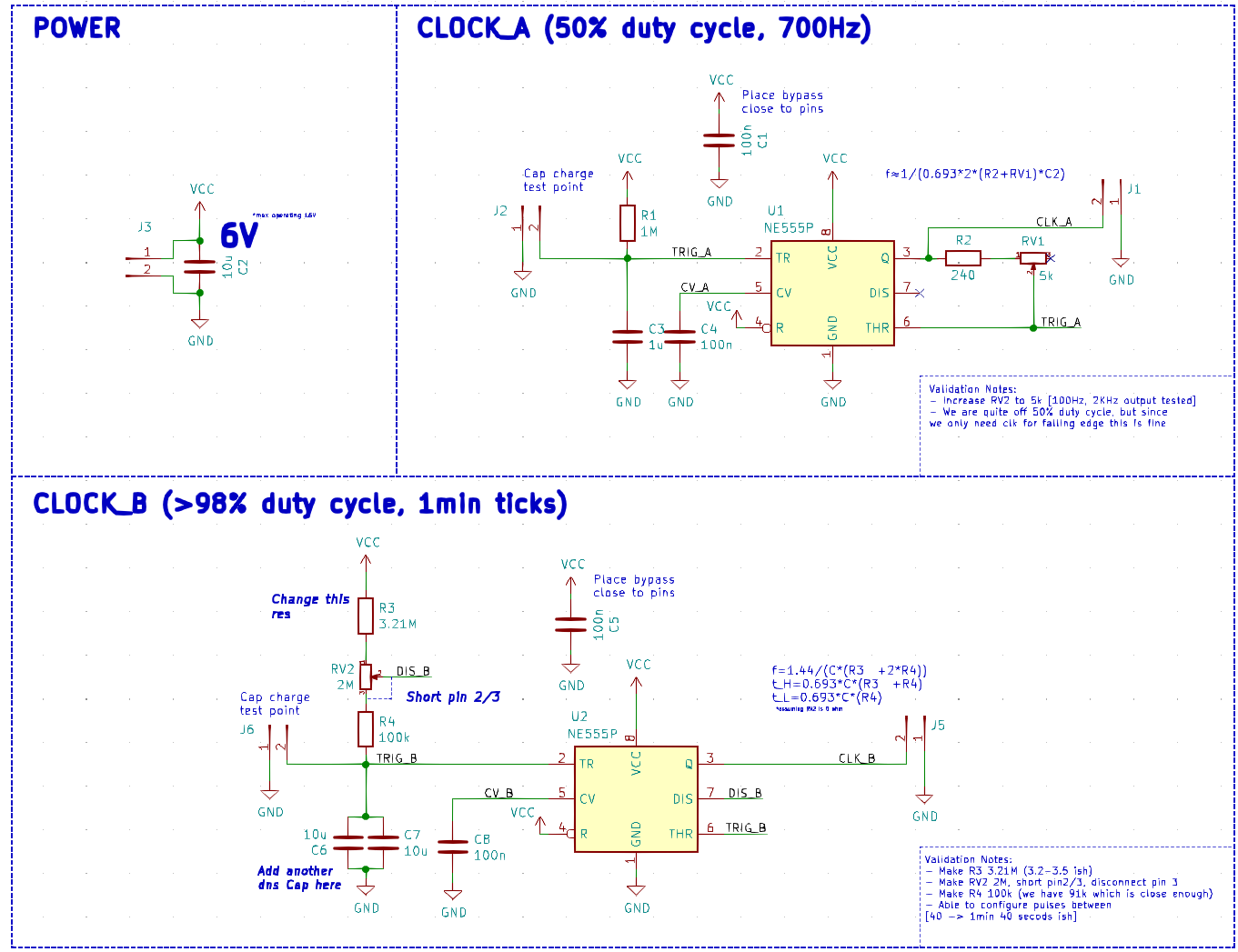
The validation Circuit schematic and pcb are shown below. There was one mistake in Clock_B’s circuit; RV2 needs to have pin 3/2 shorted, this allows us to tweak the frequency instead of just the duty cycle of the output. Other then this there were a few component value changes to allow me to hit the desired frequency in both circuits (neither circuit followed their formula particularly well).
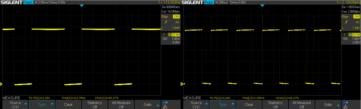
Here are some of the captures for the clock sources. Clock A can be configured between 100Hz to 2.2KHz when using a 5k potentiometer.
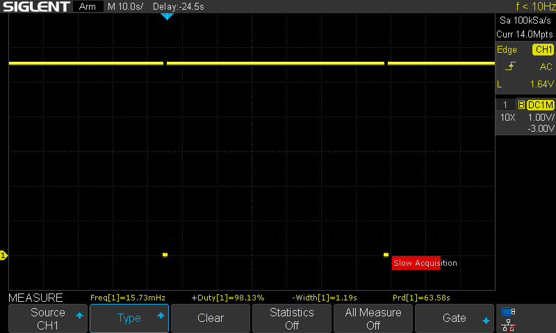
Clock B can be configured for a 45seconds to 1min 30 second period. Note the short -width is intentional.
Discussions
Become a Hackaday.io Member
Create an account to leave a comment. Already have an account? Log In.